GIMIX 64K BYTE CMOS STATIC RAM BOARD W/BATTERY BACK-UP for the SS-50/SS-50C bus
Using the latest in memory technology, the GIMIX 64K BYTE CMOS STATIC RAM BOARD combines the best features of previous memory boards on one board.
FULLY STATIC MEMORY with its inherent low soft error rate and freedom from alpha-particle induced errors. No complicated refresh timing or clocks required for data retention. Fully compatible with any of the 6800/6809 DMA techniques.
HIGH SPEED 20Oos. memorys for guaranteed operation at 2MHz. with no wait states or clock stretching required.
ULTRA-LOW POWER CMOS RAM requires less than 1/4 AMP (250 Ma.) at 8V. for a fully populated 64K BYTE board. 'Less power supply loading and heat generation for cool, efficient operation.
NON-VOLATILE using an on-board nickel-cadmium battery. The board retains data even with system power removed. With the battery fully charged, the contents of the memory remain intact for a minimum of 21 days.
HIGH DENSITY permits greater memory expansion to meet the needs of todays sophisticated, multi-user/multi-tasking operating systems.
ADDRESSABLE in two 32K sections that have their own decoding for both the regular and extended (SS-50C) address lines. Each section can be addressed to any 32K boundary in the address range (1M BYTE with extended addressing). The 32K sections are divided into four 8K blocks that can be individually enabled or disabled. Disabled sections do not occupy any address space.
RELIABLE like all GIMIX products, the 64K BYTE CMOS STATIC RAM is designed with reliability in mind. Series damping resistors, a fully gridded power and ground layout, and generous power supply decoupling, all contribute to reliability and data integrity. An unsafe voltage detect circuit inhibits writes to the board, when the 8V. supply falls below a preset level, to prevent loss of data during the transition between system and battery power.
The GIMIX 64K BYTE STATIC RAM BOARD is ideally suited to a wide variety of applications.
Its h~gh density and ultra-low power consumption make it possible to greatly expand systems with a few available bus slots and limited power supply capabilities.
The battery back-up feature is useful where data loss due to power failure cannot be tolerated, or as a replacement for disk or tape storage where conditions such as environment prohibit their use. Since the entire board can be hardware write protected by a switch located at the top of the board, it can also be used to emulate PROM or ROM memory. This is especially useful during firmware developement where frequent software changes must be made.
ADDRESSING
The board is addressed as two separate 32K blocks. DIP-switches
are used to select the base address of each block, the extended
address (55-SOC) for each block if required, and to enable or disable
8K sections within each block.
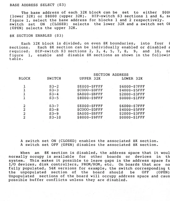
BASE ADDRESS SELECT (53)
The base address of each 32K block can be set to either $0000
(lower 32K) or $8000 (upper 32K). DIP-switch 53 sections 1 and 6, see
figure 1, select the base address for blocks 1 and 2 respectively. A
switch set ON (CLOSED) selects the lower 32K and a switch set OFF
(OPEN) selects the upper 32K.
8K SECTION ENABLES (53)
Each 32K block is divided, on even 8K boundaries, into four 8K
sections. Each 8K section can be individually enabled or disabled as
[image:2.632.52.594.121.763.2]required. DIP-switch 53 sections 2, 3~ 4, S, 7, 8, 9, and 10, see
figure 1, enable and disable 8K sections as shown in the following
table.
SECTION ADDRESS
BLOCK SWITCH UPPER 32K LOWER 32K
1 53-2 $EOOO-$FFFF $6000-$7FFF
1 53-3 $COOO-$DFFF $4000-$SFFF
1 53-4 $AOOO-$BFFF $2000-$3FFF
1 S3-S $8000-$9FFF $OOOO-$lFFF
2 53-7 $EOOO-$FFFF $6000-$7FFF
2 53-8 $COOO-$DFFF $4000-$SFFF
2 53-9 $AOOO-$BFFF $2000-$3FFF
2 53-10 $8000-$9FFF $OOOO-$lFFF
A switch set ON (CLOSED) enables the associated 8K section. A switch set OFF (OPEN) disables the associated 8K section.
When an 8K section is disabled, the address space that it would
normally occupy is available for other boards or devices in the
system. This makes it possible to leave gaps in the address space for
I/O devices, disk controllers, PROM/ROM, etc. On boards that are not
fully populated, S6K versions for example, the switch corresponding to
the unpopulated section of the board should be OFF (OPEN).
Unpopulated sections of the board will occupy .address space and cause
S3
BLOCK I
I
UPPER/LOWER 32K SELECT
I
ON (CLOSED)=LDWERBK ENABLES ON (CLOSED)= ENABLE
UL
I
4
3
2
--
-
-2
3
45
BLOCK 2
UPPER/LOWER 32K SELECT ON (CLOSED) = LOWER
8K ENABLES ON (CLOSED) = ENABLE
UL
I
4
3
2
,...----.
--
-6
7
8
9
10BASE ADDRESS SELECT
FIG. I
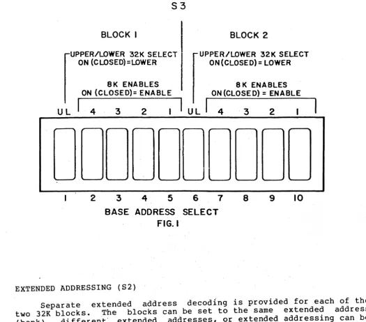
EXTENDED ADDRESSING (52)
Separate extended address decoding is provided for each of the
two 32K blocks. The blocks can be set to the same extended address
(bank), different" extended addresses, or extended addressing can be
disabled for one or both blocks. DIP-switch 52 sections I and 6, see
figure 2, enable or disable extended address decoding for blocks 1 and
2 respectively. A switch set ON (CLOSED) enables extended address
decoding for the associated block. A switch set OFF (OPEN) disables
extended address decoding for the associated block.
DIP-switch 52 sections 2, 3, 4, and 5 correspond to extended
address lines A16, A17, A18, and A19. If textended address decoding
for block 1 is enabled (52-1
=
ON), these switches must be set to thebinary equivalent of the desired bank address ($0 through $F). A
switch set ON (CLOSED) corresponds to a "1" in that bit position. A
switch set OFF (OPEN) corresponds to a "0". If extended address
decoding for block 2 is enabled (S2-6 = ON), DIP-switch 52 sections 7,
8, 9, and 10 which also correspond to extended address lines Al7
through Al9 respectively, must be set to the desired bank address for
[image:3.615.71.596.32.493.2]52
EXTENDED ADDRESS ENABLE
[
]
ON (CLOSED)= ENABLE XON
B
AI6
[
]
2L
0
EXTENDED ADDRESS C
SELECT
AI7
[
]
:3
K
ON (CLOSED)
=
"."
OFF (OPEN)=
lid'
AIS
[
]
4
AI9
[
]
5
EXTENDED ADDRESS ENAB LE
[
ON (CLOSED)
=
ENABLE XON]
6
B
AI6
(
.J
7
L
0
[
]
CEXTENDED ADDRESS
AI7
8
K
SELECT ON (CLOSED)
= "."
[
]
2OFF(OPEN)
= "
0"AI8
9
AI9
[
)
10EXTENDED ADDRESS SELECT
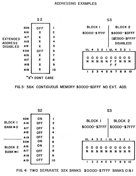
ADDRESSING EXAMPLES
Figures 3
configurations.
and 4
FJG.2
show illustrate two possible address
Figure 3 shows the proper switch settings for 56K of contiguous
memory from $0000 to $DFFF, with extended addressing disabled. Note
that switch S3 section 7, which disables the upper 8K section of block
2, must be OFF (OPEN), even if no memory chips are installed This is
the normal configuration for a 56K system using FLEX~ or OS-9~ level
1.
Figure 4 shows the proper switch settings for addressing the
board as two 32K blocks, both addressed from $0000 to $7FFF, on two
ADDRESSING EXAMPLES
52
53
XON
OFF BLOCK I BLOCK 2AI6
X2
50000- S 7FFF S8000- SDFFFEXTENDED
AI7
X 3 (SEOOO-SFFFFADDRESS
AlB
X4
DISABLED)DISABLED
AI9
X
5
XON
OFF6
UL 4
3 2
I UL 4
3 2
IAI6
X7
AI7
X
B
0 0o
0 0o
0 0 0 0N N N N N F F
N N N
AlB
X9
F FAlB
X
10I
2 3 4
5 S 7 a 9
10-x".
DONT CAREAG.
3:56K CONTIGUOUS MEMORY SOOOO-SDFFF NO EXT. ADD.
S2
S3
XON
ONBLOCK I
BLOCK 2
BLOCK I
AI6
OFF2
BANK:t$O
AI7
OFF3
SOOOO-S7FFF SOOOO-S7FFF
AlB
OFF4
AI9
OFF 5UL 4
3 2
I UL 4
3 2
I
ONXON
S
BLOCK· 2
AIS
ON7
0
0o
0 0 0
0o
0 0
BANK~I
AI7
OFF,a
N NN N
NN
N
N N
NAla
OFF9
AI9
OFF .10I
2
3 4 5
6 7 8 9
10 [image:5.634.31.590.44.769.2]WRITE PROTECT
WRITE PROTECT SWITCH (Sl)
The write protect switch (Sl), located at the upper right corner
of the board, disables the write circuitry and prevents the system
from writing data to the memory. When the switch is moved to the left
position (toward the memory array) the board is write enabled and data
can be written to as well as read from the memory. When Sl is moved
to the the right, the board is write protected and data cannot be
written to the memory.
BATTERY BACK-UP
The on-board Nickel-cadmium battery provides the power required
to retain data in the CMOS memorys when system power is removed. Data
remains intact for a minimum of 21 days with a fully charged battery.
The battery is trickle charged whenever system power is applied to the
board and the battery ON/OFF jumper is in the ON position. The
transition between system and battery power is automatic. An
adjustable unsafe voltage circuit monitors the +8V bus and inhibits
memory accesses whenever the bus voltage falls below a preset safe
level. This prevents false writes to the memory when the system bus is in an undefined state during power-up and down.
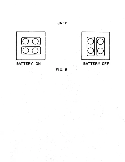
BATTERY ON/OFF JUMPER (JA-2)
JA-2 provides a means for disconnecting the battery when battery
operation is not desired or when parts are removed from or installed
in the board. Figure 5 shows the proper positions of the jumpers for
battery ON and OFF.
CAUTION: When the battery ON/OFF jumper (JA~2) is in
the ON position, power is applied to the memory array and
the CMOS decoders at all times, even when the board is
removed from the system. Before removing or installing
parts at these locations the battery ON/OFF jumper must be
placed in the OFF position to prevent possible damage to the
parts. Use caution wh~n handling the board to prevent
shorting the battery terminals together or to other parts of the circuit or damage to the battery or the board may occur.
VOLTAGE THRESHOLD ADJUSTMENT (R2)
The voltage at which the unsafe voltage detector activates is
determined by the setting of trimmer resistor R2. This adjustment is
factory set at a voltage just above the point where the on-board
voltage regulator falls out of regulation, approximately 7 volts, and
should not need readjustment under normal circumstances.
NOTE: In certain 55-50 systems with marginal power
supplies, the bus voltage may be too low to allow proper
operation of the board. These systems will require
modifications to their power supplies to provide sufficient
voltage. The nominal +8V bus voltage should be somewhat
(0 0)
(00)
BATTERY ON
JA-2
FIG. 5
00·
00
[image:7.651.65.585.84.757.2]R/W~
A.~
AI~~
AIS 6
A19~ ~~ VMA'~
t
~
dA3 51WRITE PriOT.
., '" ., "
.
"
..
RPII- RPIO-
..
", ,
.
, , , ,7
1,10,19
" " " " " .,
RPIO-,
.
, , , ,TYPICAL MEMORY ARRAY I
I
CONNECTIONS FOR EACH OECODER (U45,40,37a35)U25
~I~
WE~
:~
, "
,
U43
~f====""=-'=;-;;;:::t·:::t====l-LJ.----k~::~ ~"
E'>'
l
1
i 1---,;?:;(L'
~~Lo' ~
,----,---.----.--.,.
.,.
r---~I : U 45 ~~ U26 ~c 2r---U27
_.t:::t=t=:::t:==:j·~:'~2A f1L-U28
0& 16 011 15
" , "
03 13
1,10,19
.'"
" .'" RPI- A ,
,
"
" , ,
" " "
U49 "
"
.
U33 ,~ 36811
c;-- ,
7
1,19
7
.'" RPI- , ,
"
I'--' ,
~ "
i'---' U34 , '---' "
368 I
,
7
,
R9 ~~3
.5A PU
·OA A~
~
12 U36 3 4 U36,- G2B flL-U2.9
~3G 141 6 2 ,::'11
~ _ _ _ _ _ _ _ _ _ 32C u 1425 3 : ~
.) ~5 Ie 3 143:~§~~~.~. ~'dGG,-, l~ _________ l__-__+----~
~U30
sf.!---U31
~ I 1~U32
,-J" '" "
PO , U38'
JF'
9,,,' ;~~42:~
:
~>'~ .... ---~---,UI7
.,.
, 0 52'
., :-:t
)...J
A16
i~[t
Al7 AIS
A19 ;~ ,
;~
GND ~
)...J
.,. 1 " ,
AI6 I~
l
AI7;~
AIS :~ ,~
AI9 t~ , 7
9.-J~
~
RI'"
"
" R2
~II "
..
~
6 _\..U41
j
~
1
Jj-R6
Jj-CI
f3
f4
7
U48
."
U46
+
.'" 14 13 8 JU41 12
10
o¥ ,
~ +SA
127-c33
.
,"
","
03 13
06 IS ,,'
",jJ''-' --+--/)
03 13
t-~-~+-~. "~"L_ _ _ _ _ ~~ __________ ~~~
~r---2~ U:37 ~~~:~
---+~=t==t:=j=·fm 3~ lim 4f!!---U13 UI2
lj~U14
6~U15
~GI 7~U16 ::~ :~
"'IO~
CS 18
0717
~~ 06 16
03 Iii
04 14
"
t--+---' 1++
.1
L....~-+--ID)t3 --+-f,QQl-R5~~~---'-I'"
T
~6
\ 7D5 ['5 R4 +,,_ 81"f.
r-
C26'---t=+==t=il~ ~:'I"-'::
_______
.J!"-.-"' _ _ _ ..----JI
I
L-f---lcU35 ;t13 ~iD4
C
~~~~ 1337W.37thPLACE CHICAGOIL60609"+
~"
04 GIMIX INC .R7 <C-_J\AR31v-_ _ _ _ _ _ -®f-lQ~2r---d-AI--:-G~+7---1L-'y_~: 2-1-81 LOGIC DIAGRAM 1~----""
64K STATIC RAM
PROPRIETARY MAT'L,ALL RIGHlS
COMPONENT LAYOUT
IF S3-1 IS OFF, USE ADDRESSES LABLED I U IF S3-6 IS OFF, USE ADDRESSES LABLED 2U