Manuscript version: Author’s Accepted Manuscript
The version presented in WRAP is the author’s accepted manuscript and may differ from the published version or Version of Record.
Persistent WRAP URL:
http://wrap.warwick.ac.uk/120079
How to cite:
Please refer to published version for the most recent bibliographic citation information. If a published version is known of, the repository item page linked to above, will contain details on accessing it.
Copyright and reuse:
The Warwick Research Archive Portal (WRAP) makes this work by researchers of the University of Warwick available open access under the following conditions.
Copyright © and all moral rights to the version of the paper presented here belong to the individual author(s) and/or other copyright owners. To the extent reasonable and
practicable the material made available in WRAP has been checked for eligibility before being made available.
Copies of full items can be used for personal research or study, educational, or not-for-profit purposes without prior permission or charge. Provided that the authors, title and full
bibliographic details are credited, a hyperlink and/or URL is given for the original metadata page and the content is not changed in any way.
Publisher’s statement:
Please refer to the repository item page, publisher’s statement section, for further information.
Indirect to direct gap crossover in
two-dimensional InSe revealed by ARPES
Matthew Hamer,
†,‡Johanna Zultak,
†,‡Anastasia V. Tyurnina,
†,‡Viktor
Zólyomi,
†,‡Daniel Terry,
†,‡Alexei Barinov,
¶Alistair Garner,
§Jack Donoghue,
§Aidan P. Rooney,
§Viktor Kandyba,
¶Alessio Giampietri,
¶Abigail J. Graham,
kNatalie C. Teutsch,
kXue Xia,
kMaciej Koperski,
†,‡Sarah J. Haigh,
§,‡Vladimir I.
Fal'ko,
∗,†,‡Roman Gorbachev,
∗,†,‡and Neil R. Wilson
∗,k†School of Physics and Astronomy, University of Manchester, Oxford Road, Manchester,
M13 9PL, UK
‡National Graphene Institute, University of Manchester, Oxford Road, Manchester, M13
9PL, UK
¶Elettra - Sincrotrone Trieste, S.C.p.A., Basovizza (TS), 34149, Italy
§School of Materials, University of Manchester, Oxford Road, Manchester, M13 9PL, UK
kDepartment of Physics, University of Warwick, Coventry, CV4 7AL, UK
E-mail: *[email protected];*[email protected];
Abstract
Atomically thin lms of III-VI post-transition metal chalcogenides (InSe and GaSe) form an interesting class of two-dimensional semiconductor that feature strong varia-tions of their band gap as a function of the number of layers in the crystal14 and,
weakly indirect band gap in monolayers and bilayers.711Here, we apply angle resolved
photoemission spectroscopy with submicrometer spatial resolution (µARPES) to visu-alise the layer-dependent valence band structure of mechanically exfoliated crystals of InSe. We show that for 1 layer and 2 layer InSe the valence band maxima are away from the Γ-point, forming an indirect gap, with the conduction band edge known to
be at the Γ-point. In contrast, for six or more layers the bandgap becomes direct, in
good agreement with theoretical predictions. The high-quality monolayer and bilayer samples enables us to resolve, in the photoluminescence spectra, the band-edge exciton (A) from the exciton (B) involving holes in a pair of deeper valence bands, degenerate at Γ, with the splitting that agrees with both µARPES data and the results of DFT modelling. Due to the dierence in symmetry between these two valence bands, light emitted by the A-exciton should be predominantly polarised perpendicular to the plane of the two-dimensional crystal, which we have veried for few-layer InSe crystals.
Keywords
ARPES, indium selenide, 2D materials, density functional theory, photoluminescence, spin-orbit coupling
Two-dimensional materials (2DM) and their van der Waals heterostructures, constructed by the mechanical assembly of individual 2D crystals, have a great potential for optoelec-tronic applications.12 The fast growing family of 2DM13includes 2D insulators, 2D
semicon-ductors with various band gaps, 2D metals and even 2D superconsemicon-ductors, with electronic and optical properties that often dier from their bulk allotropes.14In this family, post-transition
metal monochalcogenides (PTMC), III-VI compounds such as GaSe and InSe, are emerging as important materials to study, due to their interesting layer-dependent optical properties and exceptionally high carrier mobility.14,8,15,16 Both GaSe and InSe display a pronounced
photolu-minescence (PL) spectroscopy of atomically thin lms of these compounds. The latter eect is partly due to the interlayer hybridisation of S-orbitals of metal atoms and Pz-orbitals of
Se dominating among the states at the edge of the conduction band at the Γ-point, where
electrons also have a light in-plane mass whose L-dependent values, determined from the
temperature variation of Shubnikov de Haas oscillations,3 coincide with the theoretically
predicted masses.11 Such a spectral evolution is accompanied by the theoretically predicted
attening of the top valence band dispersion, which has the potential to lead to a phase transition of p-doped GaSe monolayer lms into, e.g., a ferromagnetic state,9,10 but is more
likely to localise holes, as observed by systematically high (MΩrange) resistances measured
in p-doped few-layer InSe lms. Moreover, for both InSe and GaSe the valence band edge in monolayer and bilayer lms was predicted to shift away from the Γ-point, as recently
conrmed for GaSe by angle resolved photoemission spectroscopy (ARPES) studies.18,19
Here, we use ARPES to determine the valence band structure of monolayer and few-layer crystals of γ-InSe. Conventional ARPES is limited to large (typically>100µm)
atom-ically at samples, which for most atomatom-ically thin materials necessitates epitaxial growth on single crystal substrates. For this reason, previous ARPES experiments on monolayer metal monochalcogenides have used materials grown by molecular beam epitaxy.1821 Most
transport and optical investigations instead use mechanically exfoliated akes which, though higher-quality, are typically only a few µm across. We have recently demonstrated that
sub-micrometer spatially resolved ARPES (µARPES) enables high resolution measurements
from mechanically exfoliated akes.22In this way we can directly determine the valence band
electronic structure in the same samples as were used for electrical and optical studies in these 2DM. Here, we combineµARPES with optical spectroscopy and ab initio calculations
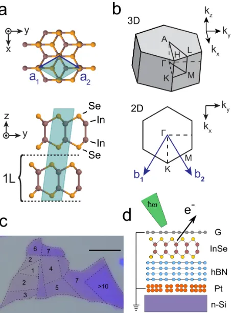
Figure 1: InSe sample structure. Crystal structure, (a), and Brillouin zone, (b), of
γ-InSe. The blue shaded regions in (a) indicate the unit cell, lattice vectors are shown in
blue. (c) Schematic of the 2D heterostructure used for ARPES measurements. (d) Optical microscope image of a mechanically exfoliated InSe ake, regions of dierent optical contrast correspond to regions of dierent thickness (scale bar 5µm).
Results and Discussion
Layers of InSe have a honeycomb atomic arrangement produced by four planes of atoms, Se-In-In-Se. Stacked in the most commonly observed γ-InSe polytype, Fig. 1a, few-layer-thick
InSe has a hexagonal 2D Brillouin zone, Fig. 1b. An optical microscope image of a typical InSe crystal produced by mechanical exfoliation onto an oxidised silicon wafer is shown in Fig. 1d, where individual1to7Lterraces were identied by their optical contrast, conrmed
by atomic force microscopy. Individual regions within the ake were identied by scanning photoemission microscopy (SPEM)22 before performing detailed ARPES studies of each
uni-form few µm area. To acquire high-resolution spectra, the akes must be transferred (see
[image:5.612.194.422.70.376.2]photoemis-sion current, and a clean surface recovered.22 To meet these criteria, mechanically exfoliated
InSe akes were sandwiched between hexagonal boron nitride or graphite underneath and an encapsulating layer of graphene on top, as shown schematically in Figure 1c. This provides charge dissipation and protects the material from decomposition during air exposure and subsequent vacuum annealing necessary to clean the surface. The stack was constructed in a puried Ar environment using a remotely controlled micromanipulation system23 that
Figure 2: γ-InSe valence band dispersion. µARPES measurement of the valence band
structure of mechanically exfoliated 1L, (a), and bulk, (d), InSe along the high symmetry directions as labelled. DFT band structures are overlaid as white (black) dashed lines for the valence (conduction) band; in (d) the blue dotted lines correspond to the theoretical predictions for kz = 0.5 and the white / black to kz = 0 in units of out-of-plane reciprocal
lattice constant. The red dashed lines are guides to the eye for the graphene bands as labelled. The experimental data has been reected about Γ in each case to aid comparison
with theory. Optical transitions corresponding to the A (B) exciton are labelled in red (blue). The photoluminescence spectrum of the monolayer is also shown, (b), along with the dependence of the optical transition energies in PL on the number of layers, (c).
Figure 2 shows the results of µARPES measurements of the valence band dispersion of
monolayer and bulk InSe, both compared to the results of DFT modelling (white dashed lines). The energy-momentum I E,kk spectra are plotted along the high-symmetry
direc-tions, as marked. In the monolayer data, Fig. 2a, graphene's π and σ bands are highlighted
by red dashed lines. For all samples measured, the Dirac point energy,ED, of the graphene
between InSe and graphene. The binding energy ofv then gives the layer-dependent valence
band oset between InSe and graphene, Table 2. The large band oset for monolayer InSe conrms a signicant Schottky barrier would be formed if graphene were used as a contact to InSe, explaining the high resistance previously reported3 (however, as we discuss below, the
band oset is smaller for few-layer crystals, in agreement with high quality tunable contacts observed in Ref.4). The measured monolayer InSe bands appear to be in a good agreement
with valence band spectra calculated using VASP code24 with experimentally measured
lat-tice parameters, as overlaid in Figure 2a. The upper valence band, labelled v, is almost at
near Γ, dispersing to higher binding energy at the Brillouin zone boundaries. Our DFT
cal-culations (see Methods) take into account spin-orbit coupling (SOC), which is necessary19,25
for the accurate description of two quadruplets of the lower-lying valence bands, v1 and v2,
dominated by the Px and Py orbitals of Se atoms. These bands are distinguished by the
z → −z mirror symmetry of their wave functions, which are even inv1 bands and odd in v2,
and each of these quadruplets is split25 by atomic SOC into two doubletsv±3 2
1,2 and v
±1 2
1,2 with
the total (spin plus orbital) angular momentum projections onto the z-axis of ±3
2 (higher
energy) and ±1
2 (lower energy), respectively. To further aid the discussion on optical
prop-erties, we also show the conduction band, c, as predicted by theory with a scissor correction
implemented11 to counter the underestimation of the gap in DFT (see Methods).
The ARPES spectra in Fig. 2a can be compared to photoluminescence (PL) observed in monolayer InSe, shown in Fig. 2b. Here, the A-exciton corresponds to the transition from
c↔ v at Γ, as marked by the red arrow on Figure 2a, and the B-exciton to the transition
c↔v±
3 2
1 , as marked by the blue arrow. Based on the PL spectrum shown in Fig. 2b, we are,
now, able to resolve A- and B-exciton lines in monolayer InSe (which was not possible in the earlier optical studies of this system3) and compare those to the ARPES data in Table
1. From the ARPES spectra we determine the energy dierence between v and the upper
doublets v±
3 2
1,2 of v1 and v2 quadruplets to be 300±100 meV (the uncertainty is large due
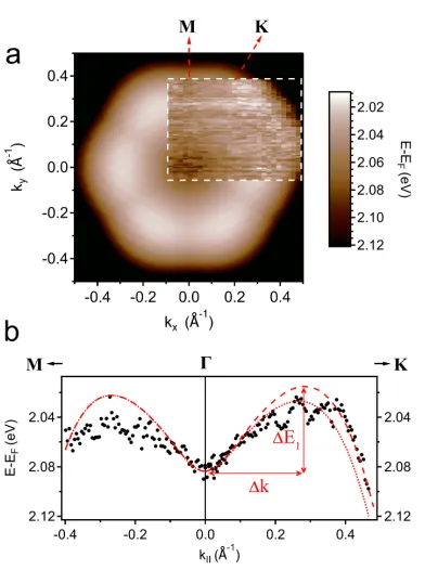
Figure 3: Valence band inversion in 1L InSe around Γ. (a) Upper valence band
energy nearΓas predicted by DFT with experimental data overlaid within the white dashed
rectangle, the color scale is identical for both and is given to the right. (b) Line proles of the upper valence band dispersion close toΓ in the M→Γ→Kdirections as marked: the
black circles are experimental data and the red dashed and dotted lines are DFT predictions for spin up and down bands.
This appears to be larger than the A-B exciton splitting, 120±70 meV, and the estimate,
170 meV, of the earlier-developed tight-binding model (TBM).25 Such a dierence can be
attributed to the hybridisation of selenium's Pz orbitals with carbon, which pushes the v
band upward, increasing its distance from v1,2 bands whose Px,y orbitals are immune to the
interlayer hybridisation.
For monolayer InSe the ARPES spectra reveal a band inversion around Γ, as shown in
detail in Figure3. The energy of the upper valence band, as predicted by DFT, is plotted as a function of kx andky in the vicinity ofΓ in Figure3a, where a lighter color corresponds to
a lower binding energy. There are six valence band maxima (VBM), each ∆k from the zone
center in theK/K0 directions, with corresponding saddle points on theΓ−M line. Within
[image:9.612.215.417.69.332.2]Methods) are overlaid, and the VBM and saddle points can be discerned despite the noise of the measurements. Line proles through both the experimental data and DFT simulations are shown in Fig. 3b, allowing the position of the VBM and the depth of the band inversion to be determined as ∆k=0.3±0.1Å−1 and ∆E1=50±20 meV respectively. In addition, we
nd that the saddle point is 20±20 meV relative to the VBM. These values agree within
uncertainty with our DFT predictions: VBM at ∆k=0.28Å−1 from Γ and ∆E1=69 meV,
with the saddle point in the M direction 7 meV higher in binding energy than the VBM,
conrming that the monolayer is, indeed, an indirect band gap semiconductor.
Table 1: InSe monolayer valence band parameters at Γ. Monolayer energy splittings
between the upper valence band and the lower valence bands, comparing the ARPES and PL data to previous25 calculations and DFT modelling in the present work.
InSe 1L v−v±
3 2
1 (meV) v
±3 2
1 −v
±1 2
1 (meV)
TBM25 170 380
DFT (this work) 310 360
ARPES 300±100 400±100
PL, XB−XA 120±70
Unlike the monolayer, bulk γ-InSe is clearly a direct band gap material, Fig. 2d, in
agreement with the existing literature.5,6,26 The ARPES spectra of a bulk crystal show
broad features with multiple states dispersed in thekz direction, perpendicular to the layers,
sinceµARPES detects photoemitted electrons with a wide (here, undetermined) range ofkz.
The white and blue dashed lines correspond to DFT band structure calculations withkz = 0
andkz = 0.5(in units of out-of-plane reciprocal lattice parameter) respectively. Where these
overlay, and are similar to the monolayer data, the bands are typically 2D in nature with little dispersion in the kz direction.
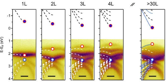
In Figure4we show how the valence band spectrum changes as a function of the number of layers in a lm. In the centre of the Brillouin zone, the valence band v is composed
Figure 4: Layer-dependent dispersion of InSe around Γ. Energy momentum slices, I E,kk, about Γ for 1L, 2L, 3L, 4L and bulk InSe as marked. Overlaid as white (black)
dashed lines are DFT predictions for the corresponding valence (conduction) band disper-sions. For bulk InSe, DFT band dispersions withkz = 0.5(in units of out-of-plane reciprocal
lattice parameter) are also overlaid as blue dotted lines. Empty red (blue) circles mark the
v (v±
3 2
1 ) band edge at Γ; lled circles mark the cband edge. Scale bars 0.2Å
−1.
in a bilayer, three in a trilayer, and so on). Simultaneously, the VBM moves to a progressively lower binding energy and gets closer to theΓ-point. For 2L InSe there remains a measurable
band inversion, with∆k=0.1±0.1Å−1 and∆E2=30±20 meV. However, for L≥3the band
inversion is no longer measurable with ∆EL≥3<20 meV, which is less than thermal energy
at room temperature. At the same time, the band gap and, consequently, A- and B-exciton energies are smaller in thicker lms, following the interlayer hybridisation of electron Pz and
S orbitals at the conductioncand valencev band edges. By comparison, theΓ-point edges of
v1 andv2 bands remain almost unchanged, due to the in-plane character of selenium's Px and
Py orbitals from which it is composed11 (see Table2). As a result, the thickness dependence
is more pronounced for A-excitons than for B-excitons, with the dierence between these two PL lines showing the same dependence on L as v −v±
3 2
1 measured using ARPES, (see
Table 1).
[image:11.612.139.473.73.238.2]Table 2: Band parameters as a function of layer number in the lm. Energies of the upper valence band (v) and lower valence band (v1) atΓmeasured by ARPES and compared
to A (XA) and B (XB) exciton energies in InSe lms with various number of layers.
−v±
3 2
1 (eV) −v (eV) XB (eV) XA (eV) v−v
±3 2
1 (eV) XB−XA (eV)
1L 2.4±0.1 2.08±0.02 2.96±0.05 2.84±0.05 0.3±0.1 0.12±0.07
2L 2.50±0.05 1.63±0.02 2.60±0.10 1.90±0.10 0.87±0.05 0.71±0.13
3L 2.54±0.05 1.47±0.02 2.60±0.09 1.67±0.08 1.07±0.05 0.93±0.12
4L 2.50±0.05 1.32±0.02 2.58±0.11 1.62±0.07 1.18±0.05 0.96±0.13
5L 2.52±0.05 1.32±0.02 2.54±0.11 1.47±0.07 1.20±0.05 1.08±0.13
7L 2.52±0.05 1.27±0.02 2.48±0.08 1.39±0.05 1.25±0.05 1.10±0.10
bulk 2.46±0.05 1.30±0.02 2.43±0.10 1.26±0.04 1.16±0.05 1.17±0.10
symmetry, and bands are either odd or even with respect to this symmetry: v and v2 bands
are even, while c and v1 are odd.11 As a result, A-exciton recombination (transitionc→v)
is coupled by electric dipole moment, dz, to the photons polarised perpendicularly to the
plane of the 2D crystal, emitting light along the plane of the InSe lm. By contrast, Px and
Py orbitals of the mirror symmetric (even) v1 band provide strong coupling of B-excitons
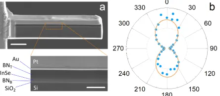
with in-plane circularly polarised photons, emitting those in the direction perpendicular to the plane of the 2D crystal. These selection rules for the interband transitions also persist in the few-layer InSe lms. To demonstrate the above-described anisotropy, we developed a modication of the conventional fabrication technique used to prepare lamellae for cross-sectional scanning transmission electron microscopy (STEM) imaging,27 whereby a block is
extracted from a hBN/InSe/hBN heterostructure using focused ion beam (see Methods) and then rotated by90◦ to allow conventional optical spectroscopy in the in-plane direction of the
InSe ake, Fig. 5a. The measured angular dependence of polarization of the emitted light, shown in Figure 5b, demonstrates strong out-of-plane linear polarisation of the A-exciton PL line.
Conclusions
Figure 5: Polarized PL emission from few-layer InSe. (a) Scanning electron micro-graphs of a lamella extracted from hBN/InSe/hBN heterostructure using focused ion beam, attached to a TEM grid. In the higher magnication view (bottom) the layers of the lamella can be resolved, including the 9L InSe ake. Scale bars are 5µm in the upper, and 1µm
in the lower micrograph. The lamella depth is ∼ 1µm. (b) Integrated intensity of A-line
photoluminescence (linear scale) as a function of detected polarization angle, excited with unpolarised light. The angles match the orientation of the SEM image in (a), with 90◦ and 270◦ corresponding to the basal plane of the InSe layer.
bilayer 2D crystals to direct gap in thicker lms. In addition, we have measured the splitting between various valence band edges in monolayers and few-layer lms. The subbands in few-layer InSe lms, determined using ARPES, agree well with the trend of a fast reduction of the band gap as the number of layers in the lm increases (from ≈2.9 eVin monolayer to
1.25 eV in bulk InSe), as observed in photoluminescence measurements. The polarisation of
the interband transition corresponding to the A-exciton conrms that the recombination of the latter emits light along the basal plane of InSe, thus, opening up a range of optoelectronic applications of InSe lms. For instance, electrical or optical pumping of InSe, deposited as a surface coating on a waveguide, would emit light along its axis and the area of such a coating can be easily scaled up to increase emission intensity (unlike other semiconducting 2DM which have to be stacked vertically to increase the brightness28) oering an opportunity
to create bre-optics-based light-emitting diodes and other light sources.
Methods
[image:13.612.193.415.75.172.2]taken from experiments:2 the in-plane lattice constant was set to 4.00Å and the inter-layer
spacing to 8.32Å. The atomic positions in the monolayer were relaxed until forces on the
atoms were below 0.005 eV/Å. The plane-wave cuto energy was 600 eV. We sampled the
Brillouin zone with a24×24×1grid for few-layer InSe, and with12×12×12for bulk.
Spin-orbit coupling was taken into account during the band structure calculations. We used the local density approximation for the exchange-correlation, which is known to underestimate band gaps hence we implemented a scissor correction by shifting the conduction band up by a constant amount such that the calculated gap in the bulk limit becomes 1.32 eV, the
estimated bulk gap at ∼100 K based on the temperature dependence of the bulk gap in
experiments.2,29,30
Sample fabrication. For µARPES, Bridgman-grown bulk rhombohedral γ-InSe
crys-tals were mechanically exfoliated onto silicon oxide and thin multi-terraced akes (1L to
10L) selected. These akes were picked up with monolayer graphene using the poly(methyl
methacrylate) (PMMA) dry peel transfer technique31stamped onto a laterally large (>50µm),
thin (<50 nm) graphite (Figure 3 and 4) or hBN (Figure 2) crystal on a Ti/Pt (3 nm /
20 nm) coated highly n-doped Si wafer. The stack was annealed at 150◦C for 1 hour, to
induce contamination trapped between the akes to agglomerate through the self-cleaning mechanism.27The exfoliations, transfers and annealing all took place within an Ar glovebox.
The thick ake analysed in Figure 2d was only partially encapsulated by graphene which is why no graphene bands are observed in the µARPES spectra.
For investigation of in-plane PL, InSe was exfoliated onto silicon oxide in an Ar glovebox. Suitably thin akes were selected by their optical contrast, picked up with thin hBN (<10 nm)
using the PMMA dry peel transfer technique,31 and stamped onto thick hBN (>100 nm) on
silicon oxide. The sample was removed from the glovebox, out-of-plane PL checked, an additional layer of thick (>100 nm) hBN transferred on top of the encapsulated InSe, and
then coated with 3 nm AuPd + 5 nm amorphous carbon for added protection. In an FEI
(∼1µm) layer was deposited on the 2D stack to act as an etch mask while a lamella was cut.
FIB milling was used to remove a cross-section, cutting around a lamella through the stack using a30 kVGa+ beam, current7 nAto dig trenches, then current1 nAto thin the lamella.
A micromanipulator was used to extract the lamella, rotate it by90◦, and position it on an
OMICRON transmission electron microscopy (TEM) grid. After milling, the damaged edges of the 2D stack were removed by FIB polishing using decreasing acceleration voltages (5 kV,
47 pA and 2 kV,24 pA). The nal thickness of the specimen was∼1µm.
µARPES. Spectra were acquired at the Spectromicroscopy beamline of the Elettra light
source.32 A Schwarzchild mirror focused27 eV linearly polarized radiation to a
submicrome-ter diamesubmicrome-ter spot, striking the sample at an angle of incidence of45◦. Photoemitted electrons
were collected by a hemispherical analyser with 2D detector which can be rotated relative to the sample normal, aligned with the sample at its eucentric position, with energy and momentum resolution of ∼50 meV and ∼0.03Å−1. Samples were annealed at up to 650 K
for > 2 hours in ultrahigh vacuum before analysis. Liquid nitrogen cooling during
mea-surement gave a nominal sample temperature of 100 K. The kinetic energy of photoemitted
electrons at the chemical potential, EF, was determined locally on the samples by tting a
Fermi function to the drop in intensity of the graphene bands at EF. The crystallographic
orientation of the akes was determined by acquiring three-dimensional energy-momentum maps, I E,kk, of the upper valence bands around Γ and identifying the high-symmetry
directions. Energy-momentum slices through the Brillouin zone in high-symmetry directions were acquired by interpolation from a series of closely-spaced detector slices along the rele-vant directions. The energy of the upper valence band for the 1L data, as shown in Figure 3, was determined by tting a Lorentzian function to energy distribution curves, I(E), at
each(kx, ky)value.
Photoluminescence spectroscopy. Monolayer PL was recorded under3.8 eVillumination at
room temperature in a Horiba LabRAM HR Evolution system with beam spot size of∼2µm,
excitation energy of2.33 eVwas used. The polarization dependence in Figure5was recorded
at 4 K under 2.4 eV and 0.4 mW unpolarised excitation with a linearly polarized detection.
Each point is the result of integration of the PL signal between 1.23 eV and 1.49 eV for the
given polarization angle.