http://wrap.warwick.ac.uk
Original citation:
Ronak, Bajaj and Fahmy, Suhaib A. (2015) Minimising DSP block usage through
multi-pumping. In: International Conference on Field Programmable Technology (FPT),
Queenstown, New Zealand, 7-9 Dec 2015
Permanent WRAP url:
http://wrap.warwick.ac.uk/74989
Copyright and reuse:
The Warwick Research Archive Portal (WRAP) makes this work by researchers of the
University of Warwick available open access under the following conditions. Copyright ©
and all moral rights to the version of the paper presented here belong to the individual
author(s) and/or other copyright owners. To the extent reasonable and practicable the
material made available in WRAP has been checked for eligibility before being made
available.
Copies of full items can be used for personal research or study, educational, or not-for
profit purposes without prior permission or charge. Provided that the authors, title and
full bibliographic details are credited, a hyperlink and/or URL is given for the original
metadata page and the content is not changed in any way.
Publisher’s statement:
“© 2015 IEEE. Personal use of this material is permitted. Permission from IEEE must be
obtained for all other uses, in any current or future media, including reprinting
/republishing this material for advertising or promotional purposes, creating new
collective works, for resale or redistribution to servers or lists, or reuse of any
copyrighted component of this work in other works.”
A note on versions:
The version presented here may differ from the published version or, version of record, if
you wish to cite this item you are advised to consult the publisher’s version. Please see
the ‘permanent WRAP url’ above for details on accessing the published version and note
that access may require a subscription.
Minimizing DSP Block Usage
Through Multi-Pumping
Bajaj Ronak
∗and Suhaib A. Fahmy
†∗School of Computer Engineering
Nanyang Technological University, Singapore Email: [email protected]
†School of Engineering, University of Warwick, UK
Abstract—Resource sharing in the mapping of an algorithm to an architecture allows the same resource to be scheduled for different uses in different cycles, generally at the cost of increased schedule length. Multi-pumping is a method whereby a resource is clocked at a frequency that is a multiple of the surrounding circuit, thereby offering multiple executions per global clock, and therefore sharing in the same clock cycle. This concept maps well to FPGA architectures, where hard macro blocks are typically capable of running at higher frequencies than standard logic. While this technique has been demonstrated for multipliers, modern DSP blocks are more complex with multiple computational nodes. In this paper, we apply multi-pumping to minimise DSP block usage, while taking advantage of the multiple nodes they support. The proposed approach uses, on average, 39% fewer DSP blocks, at a cost of 19% more LUTs and 7% more registers.
I. INTRODUCTION
As FPGAs have evolved from platforms for implementing glue logic to advanced platforms for high speed compu-tation, their architecture has gained more suitable features for algorithm implementation. Applications including digital signal processing, automotive, computer vision, and high-performance computing have driven the advancement in archi-tecture. Embedded hard blocks implement often-used functions directly in silicon, thus consuming less area and power, and running at a higher clock speed than the equivalent function in logic. On modern devices, these include memory blocks, DSP blocks, embedded processors, and more.
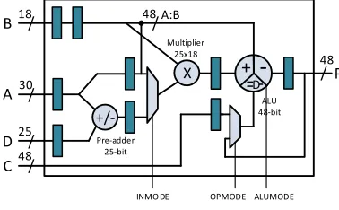
The simplified architecture of the DSP48E1 primitive in modern Xilinx FPGAs is shown in Fig. 1. Inputs A, B, C, and D are of different wordlengths:30bits,18bits,48bits, and25
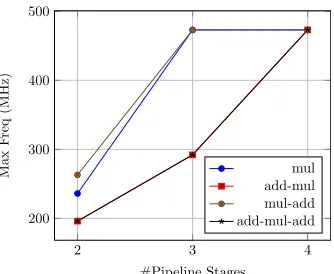
bits respectively. The DSP48E1 consists of three sub-blocks: a25-bit pre-adder, a25×18-bit multiplier, and a48-bit ALU. These sub-blocks can be combined in different ways to per-form up to three different operations using one DSP primitive. Internal pipeline registers allow the DSP blocks to achieve high throughput. Fig. 2 shows the maximum achievable frequency with use of different sub-blocks, for different pipeline depths. Maximum throughput can be achieved using three pipeline stages if the pre-adder sub-block is not used. All four pipeline stages are required when using pre-adder sub-block.
Hard blocks are typically a limited resource in most FPGAs, and hence resource sharing should be applied where possible to allow designs to make use of these resources. Traditionally, operations scheduled in non-overlapped time schedules can be mapped to the same hardware resource in the binding stage. The same hardware is re-used by adding multiplexers at the inputs and de-multiplexers at the outputs.
+/-+
-D //
/ / 18
30
25 48
/ 48 B
A
D C
P Multiplier
25x18
Pre-adder 25-bit
X / 48 A:B
ALU 48-bit
[image:2.612.349.538.207.324.2]INMO DE OPMODE ALUMODE
Fig. 1: DSP48E1 primitive structure.
One of the major disadvantage of the traditional resource shar-ing is it generally increases schedule length. Multi-pumpshar-ing is another technique that reduces DSP block utilisation, without increasing schedule length. This takes advantage of the fact that DSP blocks can typically be run at a much higher frequency that the rest of the datapath, and therefore, if clocked at a multiple frequency of the surrounding circuit, multiple operations can be scheduled in the same clock cycle. In [1], the authors demonstrated the technique by mapping two multiply operations onto a single multi-pumped DSP block per global clock. However, using only the multiplier in the DSP block leaves the other blocks unused, and hence, requires all adders to be implemented in logic.
The DSP blocks in modern Xilinx FPGAs can run at a frequency of close to 500 MHz on a Virtex 6 [2], while large circuits typically only have a frequency of 150–250 MHz. This means multi-pumping is feasible. In this paper, we present an automated tool that generates synthesisable RTL from a high-level description of a complex mathematical function. It minimises DSP block utilisation by multi-pumping DSP blocks including the pre- and post-adders. To the best of our knowledge, this is the first work in which multi-pumping has been applied to embedded DSP blocks, mapping multiple operations onto a single DSP block.
II. RELATEDWORK
A significant amount of research has been done on resource sharing at RTL level as well as in high-level synthesis [3], [4], [5]. [3] proposed an algorithm combining temporal partitioning and resource sharing to obtain a resource efficient implementa-tions. [4] proposed five heuristics for global resource sharing, minimising connection and functional resources. [5] combined module selection and resource sharing to minimise area achiev-ing minimum throughput requirements. A method to reduce resource usage by determining a pattern of operations, which is then used for efficient binding was proposed in [6].
2 3 4 200
300 400 500
#Pipeline Stages
Max
F
req
(MHz)
[image:3.612.329.561.48.192.2]mul add-mul mul-add add-mul-add
Fig. 2: Maximum frequency of a DSP48E1 for different blocks used, with different number of pipeline stages.
The concept of multi-pumping has been applied previ-ously in other areas. A common example is Double-Data-Rate (DDR) memories, that allow read/write data at double the system clock frequency. It has been extensively used in designing register files [7], and multi-port memories [8]. A white paper by Xilinx [9] used multi-pumped DSP blocks with lower input data rates than the DSP block throughput. However, this has not been incorporated in the Xilinx Vivado HLS tool. Canis et al. applied multi-pumping to reduce DSP block utilisation [1] in an open-source high-level synthesis tool for Altera FPGAs, LegUp [10]. Our work differs because we consider the DSP blocks as fully featured blocks supporting different configurations of functions rather than just multipli-ers as in that work. This offmultipli-ers more opportunities to take advantage of multi-pumping since multiple operations can be multi-pumped.
III. MULTI-PUMPEDDSP BLOCKARCHITECTURE
We have designed multi-pumped DSP blocks (mpDSPs), based on the Xilinx DSP48E1 primitive, exploiting the full set of sub-blocks. We assume the mpDSP runs at double the speed of surrounding logic, requiring two clock domains. Theoretically, an application with lower frequency require-ments could offer 4×multi-pumping, however, the overheads incurred by the data multiplexers and the increased complexity of identifying sharing possibilities in the schedule would mean diminished benefits.
A block diagram of the mpDSP is shown in Fig. 3. Clk2
is aligned with and exactly twiceClk1.Clk1 Follower follows the system clock (Clk1), and is fed to the multiplexer select signal to choose between inputs to the DSP48E1 primitive. We do not use Clk1 directly to avoid possible hold-time violations [9].
The three sub-blocks: pre-adder, multiplier, and ALU can be enabled/disabled, depending on the logic to be mapped to the mpDSP. In our mapping of operations to DSP blocks, the multiplier is always used and is always enabled. All four pipeline stages of the DSP48E1 primitive are enabled to achieve maximum frequency for Clk2. In configurations for which the ALU block is used, two extra registers are added to align the C input of the DSP48E1 primitive.
The mpDSP has a maximum of 8 inputs and 2 outputs, if all three sub-blocks are utilised. If a configuration does not utilise either the pre-adder or ALU sub-blocks, the corresponding inputs are held at zero in the instantiation of the mpDSP,
+/-+
-D
X
CONFIG
A
LU
M
O
D
E
O
P
M
O
D
E
IN
M
O
D
E
A1 B1 B2
A2 D1 D2 C1 C2 Clk1 Follower
O1
O2
[image:3.612.94.261.53.190.2]Clk1 Clk2 Clk1
Fig. 3: Multi-pumped DSP Block Architecture.
and these are then optimised away by the vendor tools. The configuration of each mpDSP is fixed by setting the INMODE, OPMODE, and ALUMODE signals according to which blocks are required. At each positive edge of the system clock (Clk1), inputs I1 (A1, B1, C1, D1) and I2 (A2, B2, C2, D2) arrive
at the multiplexers. For the first half of the system clock,
Clk1F ollowerpasses theI1inputs to the DSP48E1 primitive.
The I2 inputs are selected in the second half of the system
clock. The latency of the mpDSP is equivalent to 3 system clock cycles, after which the outputs corresponding to both sets of inputs arrive at O1 andO2.
When all four inputs are used, the mpDSP block utilises 102 LUTs, 147 registers, and 1 DSP48E1 primitive. It can run at a maximum system clock frequency of 235 MHz. The maximum frequency for a design using mpDSPs is calculated as min(fClk1, fClk2/2). On more modern devices where the
DSP block can reach 700 MHz, this translates to a 350 MHz system clock which is highly respectable.
IV. IMPLEMENTATINGMULTI-PUMPING
We adapt the tool presented in [11] to generate RTL implementations utilising mpDSP blocks. The tool takes a text file description of the algorithm, and generates synthesisable RTL implementations that map to DSP blocks. The first step extracts a dataflow graph from the description. This is then partitioned into sub-graphs, such that each sub-graph can be mapped to one of the possible DSP48E1 configurations. In this DSP dataflow graph (DDFG), each node either represents a DSP48E1 primitive configuration or an add/sub operation, which is then implemented using FPGA logic. These add/sub nodes are those in the original dataflow graph that cannot be mapped to a DSP block in combination with a multiplication operation. The DDFG is then scheduled to maximise multi-pumping. The scheduled DDFG is translated to an mpDSP Dataflow Graph (mpDDFG) for RTL generation with the extra balancing registers required to align inputs to nodes in the mpDDFG. Here, we discuss the multi-pumping optimised scheduling used.
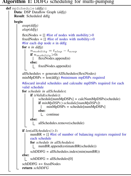
A. DSP Dataflow Graph (DDFG) Scheduling
Algorithm 1: DDFG scheduling for multi-pumping defmpSchedule(ddfg):
Data: DSP Dataflow Graph (ddfg)
Result: Scheduled ddfg
begin asap(ddfg) alap(ddfg)
flexiNodes = []#list of nodes with mobility>0
fixedNodes = []#list of nodes with mobility=0
#for each dsp nodenin ddfg
forn in ddfg:
nmobility=talap−tasap ifnmobility>0:
flexiNodes.append(n)
else:
fixedNodes.append(n)
allSchedules = generateAllSchedules(flexiNodes)
minMpDSPs = len(ddfg)#minimum mpDSPs required
#discard invalid schedules and calcualte mpDSPs required for each valid schedule
forschedule in allSchedules: ifisValid(schedule):
schedule[numMpDSPs] = calcNumMpDSPs(schedule)
ifminMpDSPs>schedule[numMpDSPs]:
minMpDSPs = schedule[numMpDSPs]
else:
continue
else:
allSchedules.remove(schedule)
iflen(allSchedules)>1:
numBR = []#list of number of balancing registers required for
each schedule
forschedule in allSchedules:
numBR.append(estimateBR(schedule))
schDDFG = allSchedules.index(min(numBR))
else:
schDDFG = allSchedules[0] schDDFG += fixedNodes
returnschDDFG
mpDSP usage, we choose the one that consumes fewer extra registers to balancing pipeline stages.
Firstly, the ASAP and ALAP schedules of the DDFG are determined to compute the mobility of each node. This is the measure of flexibility with which the node can be scheduled in different STs; the difference between the ALAP and ASAP STs. Nodes with zero mobility are those which must be scheduled in a particular ST to maintain data dependencies. Nodes with non-zero mobility can be exploited to arrive at a schedule which maximises opportunities for multi-pumping.
Nodes with non-zero mobility and all possible schedules are generated, taking into account these mobilities. This ex-haustive list of schedules ignores dependencies. The next step is to discard schedules that do not satisfy dependencies. For the remaining valid schedules, we calculate the mpDSP block requirement for each schedule. We also keep track of the minimum number of mpDSPs required (minMpDSPs) among all the schedules. Since the primary goal is to minimise usage of DSP48E1 primitives, we select all schedules that require
minMpDSPs blocks and discard others. This can result in multiple schedules with the same mpDSP consumption. To resolve this tie, we estimate the number of pipeline balancing registers required for each schedule. These are required to ensure that dataflows through the graph are correctly aligned. The schedule requiring the minimum number of balancing registers is then selected as the final schedule. If multiple schedules are equivalent at this point, the first is chosen. The algorithm is detailed in Algorithm 1.
[image:4.612.52.300.61.394.2]Although this approach results in an optimised schedule,
TABLE I: Resource usage and maximum frequency for multi-pumped DSP block.
Sub-blocks used DSPs LUTs Eq LUTs Reg Freq (MHz)
Mul 1 45 241 51 235
Pre adder-Mul 1 70 266 51 230
Mul-ALU 1 69 265 147 227
Pre adder-Mul-ALU 1 102 298 147 229
the exhaustive search does not scale well to large dataflow graphs. However, for our benchmark set, with dataflow graphs of up to 34 nodes, the algorithm is able to generate the best schedule in a reasonable time of a few seconds.
V. EXPERIMENTALSTUDY
To explore the effectiveness of the proposed multi-pumping technique and to compare against multiplier-only multi-pumping, we implemented a number of benchmark multiply-add flow graphs. Our benchmark suite include the mibench2 filter, quadratic spline, and the Savitzky-Golay filter from [12]; the ARF, EWF, horner bezier, and motion vector from [13]; and 3 polynomials of varied complexity from the Polynomial Test Suite [14]. These benchmarks represents computational kernels within a larger application. We run the adapted tool on an Intel Xeon E5-2695 running at 2.4 GHz with 16 GB RAM. All implementations target the Virtex 6 XC6VLX240T-1 FPGA found on the ML605 development board, and use Xilinx ISE 14.6.
Multi-pumping results in a trade-off between DSP blocks and LUT usage. As DSP blocks and LUTs cannot be compared directly, and to understand overall resource usage, we compare the area in terms of equivalent LUTs, where LUTeqv =
nLUT +nDSP ×(196). 196 is the ratio of the number of LUTs (150720) to the number of DSP blocks (768) on the target device. This gives a proxy for overall area consumption.
Table I shows the resource usage and maximum frequency for mpDSPs. Each row represents a combination of sub-blocks used. The number of LUTs required increases as more sub-blocks are used since more multiplexers are required at the inputs. Configurations using the ALU sub-block require 2 extra 48-bit registers to balance theCinput of the DSP48E1. Using an mpDSP results in a reduction of one DSP48E1 primitive at the cost of an increase in LUT and register usage, however the increase in LUT usage is always less than the equivalent LUT usage of a DSP block (196), hence always resulting in an equivalent LUT improvement with extra register utilisation. The maximum frequency achieved by all configurations is largely the same.
We implement three different scenarios to understand the benefits of multi-pumping full DSP blocks. The first (Original) does not use multi-pumping but maps efficiently to DSP blocks, as described in [11]. The second (MulOnly MP) multi-pumps only multipliers (similar to the method proposed in [1]). The third (MP) is the proposed multi-pumping of full DSP blocks.
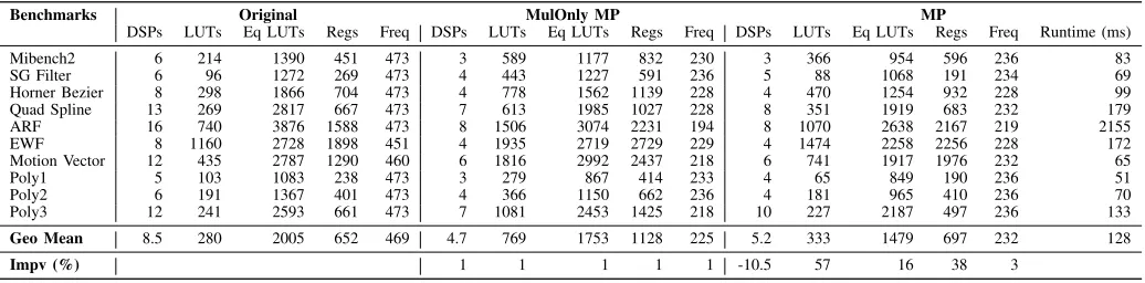
TABLE II: Resource usage and maximum frequency for 10 benchmarks. Frequency in MHz.
Benchmarks Original MulOnly MP MP
DSPs LUTs Eq LUTs Regs Freq DSPs LUTs Eq LUTs Regs Freq DSPs LUTs Eq LUTs Regs Freq Runtime (ms)
Mibench2 6 214 1390 451 473 3 589 1177 832 230 3 366 954 596 236 83
SG Filter 6 96 1272 269 473 4 443 1227 591 236 5 88 1068 191 234 69
Horner Bezier 8 298 1866 704 473 4 778 1562 1139 228 4 470 1254 932 228 99
Quad Spline 13 269 2817 667 473 7 613 1985 1027 228 8 351 1919 683 232 179
ARF 16 740 3876 1588 473 8 1506 3074 2231 194 8 1070 2638 2167 219 2155
EWF 8 1160 2728 1898 451 4 1935 2719 2729 229 4 1474 2258 2256 228 172
Motion Vector 12 435 2787 1290 460 6 1816 2992 2437 218 6 741 1917 1976 232 65
Poly1 5 103 1083 238 473 3 279 867 414 233 4 65 849 190 236 51
Poly2 6 191 1367 401 473 4 366 1150 662 236 4 181 965 410 236 70
Poly3 12 241 2593 661 473 7 1081 2453 1425 218 10 227 2187 497 236 133
Geo Mean 8.5 280 2005 652 469 4.7 769 1753 1128 225 5.2 333 1479 697 232 128
Impv (%) 1 1 1 1 1 -10.5 57 16 38 3
2.8×and 1.7×respectively. The significant increase in LUTs and registers is due to DSP blocks being used for multiplication only and all add/sub blocks being implemented in LUTs. Despite this significant increase, multi-pumping results in an average reduction in equivalent LUTs of 13%, and achieves al-most half the maximum frequency of theOriginal(225 MHz). With an overall target design frequency in the range of 150-250 MHz, this suggests multi-pumping is feasible.
Considering MulOnly MP as the baseline, MP utilises 10.5% more DSP blocks due to limited possibilities for multi-pumping. However, as full DSP blocks are multi-pumped, add/sub blocks are included, significantly reducing resource consumption. MP utilises 57% fewer LUTs and 38% fewer registers compared to MulOnly MP, with an improvement in average maximum frequency of 3%. Compared to Original,
MP results in a 39% reduction in DSP block usage with an increase of 19% and 7% in LUTs and registers respectively, effectively saving 26% equivalent LUT area. This represents DSP block savings comparable to MulOnly MP with signifi-cantly less impact on LUTs and registers.
The last column of Table II shows the time taken to generate synthesisable RTL from the high-level description for
MP, averaged over 100 executions. Runtimes vary from 51 ms to 2.2 s, with an average of 128 ms across all benchmarks, which is reasonable for a small step of the design flow.
As discussed earlier, multi-pumping is feasible only if the maximum frequency requirement of the full system is in the range of 150–250 MHz for our target device. Here, we are focused on the area efficient implementation of a computationally intensive inner loop of a larger system. As the DSP48E1 primitive in the Virtex 6 can run at a maximum frequency of 473 MHz (Fig. 2), implementations with multi-pumping achieve a maximum frequency of up to 236 MHz (half of the maximum frequency of DSP48E1 primitive) in the system clock domain. As shown in Table II, most multi-pumped implementations achieve this frequency requirement, within a margin of 2–4%.
VI. CONCLUSIONS ANDFUTUREWORK
We have demonstrated the concept of multi-pumping ap-plied to the DSP blocks in modern Xilinx FPGAs. Since these blocks can run at high frequencies, we clock them at double the system clock, and allow two DSP block functions to share a single primitive. Crucially, we multi-pump multiple nodes to fit the capabilities of these DSP blocks, resulting in average equivalent LUT area usage 26% lower than designs without
multi-pumping. We intend to explore this idea further by exploiting the dynamic reprogrammability of the DSP blocks as in [15] to increase opportunities for multi-pumping, while also developing a more efficient scheduling approach.
REFERENCES
[1] A. Canis, J. H. Anderson, and S. D. Brown, “Multi-pumping for re-source reduction in FPGA high-level synthesis,” inDesign, Automation Test in Europe Conference Exhibition (DATE), March 2013, pp. 194– 197.
[2] Xilinx Inc.,UG479: 7 Series DSP48E1 Slice User Guide, 2013. [3] J. Cardoso, “Novel Algorithm Combining Temporal Partitioning
and Sharing of Functional Units,” in IEEE Symposium on Field-Programmable Custom Computing Machines, March 2001, pp. 31–40. [4] S. Memik, G. Memik, R. Jafari, and E. Kursun, “Global resource sharing for synthesis of control data flow graphs on FPGAs,” inProceedings of Design Automation Conference, June 2003, pp. 604–609.
[5] W. Sun, M. Wirthlin, and S. Neuendorffer, “FPGA Pipeline Synthesis Design Exploration Using Module Selection and Resource Sharing,”
IEEE Transactions on Computer-Aided Design of Integrated Circuits and Systems, vol. 26, pp. 254–265, 2007.
[6] J. Cong and W. Jiang, “Pattern-based Behavior Synthesis for FPGA Resource Reduction,” in Proceedings of ACM/SIGDA Symposium on Field Programmable Gate Arrays, 2008, pp. 107–116.
[7] H. Yantir, S. Bayar, and A. Yurdakul, “Efficient Implementations of Multi-pumped Multi-port Register Files in FPGAs,” in Euromicro Conference on Digital System Design (DSD), Sept 2013, pp. 185–192. [8] C. E. Laforest, M. G. Liu, E. R. Rapati, and J. G. Steffan, “Multi-ported Memories for FPGAs via XOR,” in Proceedings of the ACM/SIGDA International Symposium on Field Programmable Gate Arrays, 2012, pp. 209–218.
[9] R. P. Tidwell,XAPP706: Alpha Blending Two Data Streams Using a DSP48 DDR Technique, Xilinx Inc, 2005.
[10] A. Canis, J. Choi, M. Aldham, V. Zhang, A. Kammoona, J. H. Anderson, S. Brown, and T. Czajkowski, “LegUp: high-level synthesis for FPGA-based Processor/Accelerator systems,” inProceedings of the International Symposium on Field Programmable Gate Arrays (FPGA), 2011, pp. 33–36.
[11] B. Ronak and S. Fahmy, “Mapping for maximum performance on FPGA DSP blocks,”IEEE Transactions on Computer-Aided Design of Integrated Circuits and Systems, vol. 35, 2016.
[12] S. Gopalakrishnan, P. Kalla, M. Meredith, and F. Enescu, “Finding linear building-blocks for RTL synthesis of polynomial datapaths with fixed-size bit-vectors,” inProceedings of IEEE/ACM International Con-ference on Computer-Aided Design, Nov 2007, pp. 143–148. [13] C. Lee, M. Potkonjak, and W. Mangione-Smith, “MediaBench: a tool
for evaluating and synthesizing multimedia and communications sys-tems,” inProceedings of International Symposium on Microarchitecture, Dec 1997, pp. 330–335.
[14] “[Online] Polynomial Test Suite,” http://www-sop.inria.fr/saga/POL/. [15] H. Y. Cheah, F. Brosser, S. A. Fahmy, and D. L. Maskell, “The iDEA