Kinetics of Solid-State Reactive Diffusion in the Cu
/
Zn System
Yoshiki Takamatsu
1, Minho O
2and Masanori Kajihara
2,*1Graduate School, Tokyo Institute of Technology, Yokohama 226–8502, Japan
2Department of Materials Science and Engineering, Tokyo Institute of Technology, Yokohama 226–8502, Japan
The kinetics of the solid-state reactive diffusion between pure Cu and Zn was experimentally examined using sandwich Zn/Cu/Zn diffu-sion couples prepared by a diffudiffu-sion bonding technique. The diffudiffu-sion couples were isothermally annealed in the temperature range of 523– 623 K for various times up to 49 h. Owing to annealing, an intermetallic layer consisting of the γ and ε phases was formed at the original inter-face in the diffusion couple, where the thickness is much smaller for the ε phase than for the γ phase. The total thickness of the intermetallic layer increases in proportion to a power function of the annealing time. The exponent of the power function takes values of 0.60–0.62 at 523– 623 K. These values of the exponent indicate that volume diffusion predominantly controls the layer growth and interface reaction partially contributes to the rate-controlling process. [doi:10.2320/matertrans.M2016278]
(Received August 3, 2016; Accepted October 7, 2016; Published December 2, 2016)
Keywords: reactive diffusion, metallization, solder, conductor, intermetallic compounds
1. Introduction
In the binary Sn–Zn system, the eutectic reaction L → Sn + Zn occurs at a temperature of Te = 472 K.1) Here, the concen-tration of Zn in the liquid (L) phase is 15 at% (9 mass%), the solubility of Zn in the Sn phase is smaller than 1 at%, and that of Sn in the Zn phase is negligible. Since the eutectic
tem-perature Te is much lower than the melting temperature of
pure Sn with Tm = 505 K, the eutectic Sn–Zn alloy is used as
a Pb-free Sn-base solder with low-melting temperature in the electronics industry.2–8) On the other hand, Cu-base alloys are widely utilized as conductor materials owing to high electri-cal conductivity. If the Cu-base conductor is interconnected with the Sn–Zn solder, various compounds are formed at the interconnection between the conductor and the solder during soldering and then gradually grow during energization heat-ing at solid-state temperatures. Since such compounds may be brittle and will possess high electrical resistivities, their growth can deteriorate the mechanical and electrical proper-ties of the interconnection.
The solid-state reactive diffusion in the Cu/(Sn–Zn) sys-tem was experimentally studied by Shohji et al.4) In their ex-periment, Cu/(Sn–Zn) diffusion couples were prepared from pure Cu and an eutectic Sn–Zn solder by a soldering tech-nique and then isothermally annealed at temperatures of T = 373–423 K. According to their observation, the region with the composition Cu0.55Sn0.41Zn0.04 consisting of the Cu, β and γ phases is formed at the original interface of the diffu-sion couple during annealing. Furthermore, the region with the composition Cu0.64Sn0.34Zn0.02 is produced at the inter-face between the Cu0.55Sn0.41Zn0.04 region and the Cu phase. Thus, rather complicated microstructure evolution takes place for the solid-state reactive diffusion in the Cu/(Sn–Zn) sys-tem. In order to understand the mechanism of such micro-structure evolution, information on the solid-state reactive diffusion in the Cu/Sn and Cu/Zn systems is necessary.
For the Cu/Sn system, the kinetics of solid-state reactive diffusion was observed in a previous study.9) In this observa-tion, Sn/Cu/Sn diffusion couples were prepared by a
diffu-sion bonding technique and then isothermally annealed in the temperature range of T = 433–473 K. In this temperature range, an intermetallic layer composed of Cu6Sn5 and Cu3Sn is formed at the original Cu/Sn interface in the diffusion cou-ple. The total thickness of the Cu6Sn5 and Cu3Sn layers in-creases in proportion to a power function of the annealing time. The exponent of the power function is close to 0.5 at T = 473 K but becomes 0.37 and 0.43 at T = 433 and 453 K,
re-spectively. Thus, in the Cu/Sn system,9) the growth of the
intermetallic layer is controlled by volume diffusion at T = 473 K but by volume and boundary diffusion at T = 433 and 453 K.
In contrast, the solid-state reactive diffusion in the Cu/Zn
system was experimentally studied by Hoxha et al.10) In their
study, Cu/Zn diffusion couples were prepared by a diffusion bonding technique and then isothermally annealed at tem-peratures of T = 523–653 K. Their study indicates that a com-pound layer consisting of the γ and ε phases is produced at the original interface of the diffusion couple during anneal-ing. The total thickness of the γ and ε layers is almost propor-tional to the square root of the annealing time at T = 653 K. On the other hand, at T = 523–623 K, raw experimental val-ues for thicknesses of the γ and ε layers are not indicated in their article.10) Nevertheless, they mention that the thickness rather linearly increases in proportion to the annealing time in the early stages at T = 523–623 K. This means that the layer growth is controlled by volume diffusion at T = 653 K but by interface reaction in the early stages at T = 523–623 K. Al-though the diffusion rate-controlling process will be realized also in the late stages at T = 523–623 K, reliable information on the rate-controlling process is lacking at these tempera-tures. To obtain such information, the kinetics of the sol-id-state reactive diffusion in the Cu/Zn system was experi-mentally observed in the temperature range of T = 523–623 K in the present study.
2. Experimental
Sheet specimens with size of 20 mm × 7 mm × 1 mm were cut from a pure Cu commercial sheet with dimensions of
300 mm × 100 mm × 1 mm and purity of 99.96% and then
*
separately annealed in evacuated silica capsules at 1173 K for 2 h, followed by air cooling without breaking the capsules.
The two surfaces with area of 20 mm × 7 mm of each
an-nealed Cu sheet specimen were mechanically polished on #800–4000 emery papers until a depth of 100 μm and then finished using diamond with diameter of 1 μm.
Sheet specimens with size of 12 mm × 5 mm × 1 mm were cut from a pure Zn commercial sheet with dimensions of
200 mm × 200 mm × 1 mm and purity of 99.5% and then
separately annealed in evacuated silica capsules at 623 K for 2 h, followed by air cooling without breaking the capsules.
The two surfaces with area of 12 mm × 5 mm of each
an-nealed Zn sheet specimen were mechanically polished on #800 emery paper. One of the two polished surfaces was again mechanically polished on #1500–4000 emery papers until a depth of 100 μm and then finished using diamond with diameter of 1 μm.
After finishing, a Cu sheet specimen was immediately sandwiched between the finished surfaces of two freshly pre-pared Zn sheet specimens in ethanol by the technique used in
a previous study.9) The sandwich Zn/Cu/Zn couples were
completely dried and then heat treated for diffusion bonding in an evacuated silica tube at temperatures of 523 K, 573 K and 623 K for times of 2 h, 0.5 h and 0.5 h, respectively, fol-lowed by air cooling. After the heat treatment, the diffusion couples were isothermally annealed at 523 K, 573 K and 623 K for various times up to 47 h. The summation of the heat-treating and annealing times is hereafter merely called the annealing time t, and the annealing temperature is denot-ed by T. Cross-sections of the annealdenot-ed diffusion couple were mechanically polished using diamond with diameters of 15 μm, 3 μm and 1 μm, and then finished with an OP-S liquid manufactured by Struers Ltd. The microstructure of the cross-section was observed by differential interference con-trast optical microscopy (DICOM). Concentrations of Cu and Zn in each phase on the cross-section were measured by elec-tron probe microanalysis (EPMA) using pure Cu and Zn with purity of 99.99% as standard specimens under the following conditions: the accelerating voltage was 20 kV; the probe cur-rent was 5 nA; the analyzing crystal was lithium fluoride
(LiF) for Cu–Kα and Zn–Kα; and the chemical composition
was evaluated by a standard ZAF correction technique.
3. Results and Discussion
3.1 Microstructure
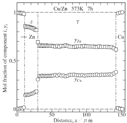
A typical cross-sectional DICOM image of the diffusion couple annealed at T = 623 K for t = 1 h (3.6 ks) is shown in Fig. 1. For this DICOM image in Fig. 1, the top and bottom regions are the Zn and Cu specimens, respectively. As can be seen, layers with different contrasts are formed at the original Cu/Zn interface. To identify each layer, concentration pro-files of Cu and Zn were measured by EPMA along the direc-tion normal to the original interface. A result of the diffusion couple with T = 573 K and t = 7 h (25.2 ks) is indicated in Fig. 2. In this figure, the ordinate and the abscissa show the
mol fraction yi of component i and the distance x measured
from an arbitrary origin, respectively, and open circles and squares represent the mol fractions yCu and yZn, respectively. As can be seen, the layers on the Cu and Zn sides are the γ
and ε phases, respectively. The thickness is smaller for the ε phase than for the γ phase. Similar results were obtained for all the diffusion couples annealed at T = 523–623 K. If we observe the edge of diffusion couple on the cross-section, we can find the location of the original Cu/Zn interface. This ob-servation indicates that the γ and ε phases grow mainly into the Zn specimen but slightly towards the Cu specimen. Con-sidering the mass conservation, we may expect that the Mat-ano interface is located in the γ layer and thus migrates from the original interface towards the Zn side. According to a
re-cent phase diagram in the binary Cu–Zn system,11) the β
phase as well as the γ and ε phases should appear as a stable
intermediate phase at T = 523–623 K. However, the β phase
was not recognized in any annealed diffusion couples in the present study. For reactive diffusion in binary alloy systems, the growth rate of an intermediate phase is predominantly de-termined by the interdiffusion coefficient of the growing phase.12–22) If the interdiffusion coefficient of an intermediate phase is small at an experimental annealing temperature, the intermediate phase cannot grow to visible thicknesses within realistic annealing times.12–22) Consequently, the
interdiffu-sion coefficient of the β phase must be much smaller than
those of the γ and ε phases. Furthermore, according to the results in Figs. 1 and 2, the interdiffusion coefficient has to be Fig. 1 Cross-sectional DICOM image of diffusion couple annealed at T =
623 K for t = 1 h (3.6 ks).
[image:2.595.322.532.71.195.2] [image:2.595.320.531.246.450.2]smaller for the ε phase than for the γ phase.
3.2 Growth behavior of intermatellic layer
As shown in Fig. 1, a tow-phase layer consisting of the γ and ε phases is formed at the original Cu/Zn interface in the diffusion couple due to isothermal annealing at T = 523– 623 K. Hereafter, the two-phase layer is merely called the intermetallic layer. From DICOM images, such as that indi-cated in Fig. 1, the area Aj of the intermetallic layer corre-sponding to the partial length wj of the original Cu/Zn inter-face was measured for cross-section j. The sums A and w
were obtained by the equations9)
A= m
j=1
Aj (1a)
and
w= m
j=1
wj (1b)
from Aj and wj, respectively, where wj = 422 μm and m ≥ 5. Using the values of A and w, the total thickness l of the inter-metallic layer was evaluated at each annealing time t as fol-lows:9)
l= A
w. (2)
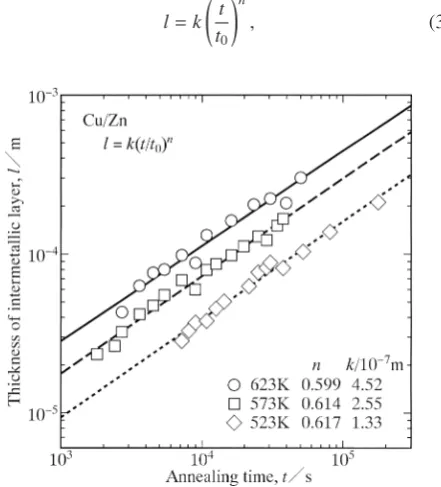
The results for T = 523, 573 and 623 K are shown as open rhombuses, squares and circles, respectively, in Fig. 3. In this figure, the ordinate and the abscissa indicate the logarithms of l and t, respectively. As can be seen, the thickness l monotoni-cally increases with increasing annealing time t. Furthermore, at T = 523–623 K, the experimental points for each annealing temperature lie well on a straight line. Consequently, l is ex-pressed as a power function of t as follows
l=k t t0
n
, (3)
where t0 is unit time, 1 s, which is adopted to make the
argu-ment t/t0 of the power function dimensionless. The
propor-tionality coefficient k has the same dimension as the thickness l, and the exponent n is dimensionless. The dimensionless argument of the power function is essentially important; oth-erwise the dimension of k varies depending on the value of n. From the experimental points in Fig. 3, k and n were evaluat-ed by the least-squares method as indicatevaluat-ed with various straight lines. The evaluated values of k and n are also shown in Fig. 3. According to the evaluation at T = 523–623 K, the overall growth rate of the intermetallic layer monotonically increases with increasing annealing temperature T.
According to Fig. 1, each compound is clearly distin-guished in the intermetallic layer. From DICOM images, such
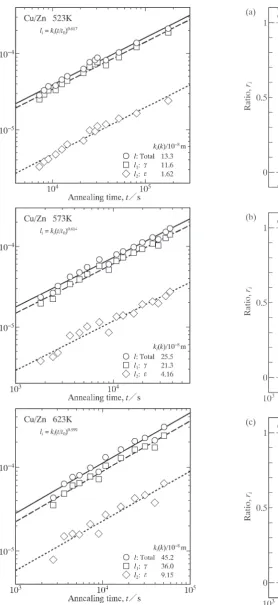
as that shown in Fig. 1, the mean thickness li of compound
layer i in the intermetallic layer was evaluated using the rela-tionships similar to eqs. (1a), (1b) and (2), where i = 1 and 2 for the γ and ε phases, respectively. Thus, there exists the following relationship among l, l1 and l2.
l=l1+l2 (4)
The results of l, l1 and l2 are shown as open circles, squares and rhombuses, respectively, in Fig. 4. In this figure, like Fig. 3, the ordinate and the abscissa indicate the logarithms of li and t, respectively. Figure 4(a), 4(b) and 4(c) shows the re-sults for T = 523, 573 and 623 K, respectively. Although the open rhombuses are slightly scattered due to small values of
l2, most of the open symbols are located well on the
corre-sponding straight line. Therefore, we consider that li is
ex-pressed as a power function of t by the following equation of the same formula as eq. (3).
li=ki tt
0
n
(5)
From the experimental points in Fig. 4, ki and n for li in eq. (5) were evaluated by the least-squares method as shown with various straight lines. Since l1 and l2 are smaller than l, how-ever, the values of k1, k2 and n for l1 and l2 cannot be estimat-ed with the same reliability as those of k and n for l. Conse-quently, using the same value of n as l, k1 and k2 for l1 and l2 in eq. (5) were estimated from the open squares and rhombus-es by the least-squarrhombus-es method as indicated with dashed and dotted lines, respectively. The values of n, k, k1 and k2 are shown in Fig. 4. As can be seen, k2 is smaller than k1 at T = 523–623 K. Although the identical value of n was adopted for l1, l2 and l, k1, k2 and k were independently evaluated from the corresponding experimental points in Fig. 4 as mentioned earlier. As a result, the relationship k = k1 + k2 does not neces-sarily hold, even though eq. (4) holds at each experimental annealing time.
At each experimental annealing time, the ratio ri of the thickness li to the total thickness l was evaluated by the equa-tion
ri=lli. (6)
The values of r1 and r2 are plotted against the annealing time t as open circles and squares, respectively, in Fig. 5. Fig-ure 5(a), 5(b) and 5(c) shows the results for T = 523, 573 and 623 K, respectively. As indicated in Fig. 4, l2 is smaller than Fig. 3 The total thickness l of the intermetallic layer versus the annealing
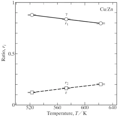
[image:3.595.64.285.508.752.2]l1. Consequently, r2 is smaller than 0.5, but r1 is greater than 0.5. Although the open symbols are slightly scattered in Fig. 5, we may consider that ri is constant independent of t for
each annealing temperature. The mean values of r1 and r2
were estimated from the open circles and squares,
respective-ly, as shown with horizontal solid and dashed lines,
respec-tively, in Fig. 5. The mean values of r1 and r2 are plotted
against the annealing temperature T as open circles and squares, respectively, with error bars in Fig. 6. Here, the error Fig. 4 The thicknesses l, l1 and l2 versus the annealing time t shown as open
circles, squares and rhombuses, respectively: (a) 523 K, (b) 573 K and (c)
623 K. Fig. 5 The ratios r1 and r2 in eq. (6) versus the annealing time t shown as
[image:4.595.77.356.64.671.2] [image:4.595.314.529.67.687.2]bar indicates the standard error. As the annealing temperature T increases, the value of r1 decreases but that of r2 increases.
Hence, the difference between r1 and r2 monotonically
de-creases with increasing annealing temperature. As a conse-quence, it is concluded that the temperature dependence of the growth rate is more remarkable for the ε phase than for the γ phase.
3.3 Rate-controlling process of intermetallic growth
The values of n in Fig. 3 are plotted against T as open cir-cles with error bars in Fig. 7. If the growth of the intermetallic layer is controlled by volume diffusion, n is equal to 0.5.12–22) On the other hand, n is equivalent to unity, if interface reac-tion governs the layer growth.23–28) According to the result in Fig. 7, n takes intermediate values between 0.5 and unity. This means that both volume diffusion and interface reaction contribute to the rate-controlling process of the layer growth at T = 523–623 K. Since the ratios r1 and r2 are constant
inde-pendent of t at each annealing temperature as shown in Fig. 5, the same rate-controlling process works for both the γ and ε phases. Such a mixed rate-controlling process of solid-state reactive diffusion was observed for various metal systems in previous studies.23–28) The values n = 0.60–0.62 are closer to 0.5 than to unity, and hence the contribution of volume diffu-sion is more predominant than that of interface reaction. As previously mentioned, the intermetallic layer grows mainly towards the Zn side and merely slightly towards the Cu side. Therefore, the Zn/ε interface is mobile, but the Cu/γ inter-face is rather stationary. Consequently, it is plausible that the interface reaction at the mobile Zn/ε interface dominantly influences the rate-controlling process of the layer growth. As previously mentioned, on the basis of the mass conservation, it is expected that the Matano interface lies in the γ layer and thus migrates from the original interface towards the Zn side. If only volume diffusion is the rate-controlling process of the layer growth, the interdiffusion coefficient of each phase is
determined by an appropriate method.29) Unfortunately,
how-ever, the mixed rate-controlling process governs the layer growth as mentioned earlier. Therefore, the interdiffusion co-efficient cannot be determined in a straightforward manner.
As mentioned in Section 1, the solid-state reactive diffu-sion in the Cu/Zn system was experimentally observed also
by Hoxha et al.10) In their experiment, Cu/Zn diffusion
[image:5.595.64.274.306.510.2]cou-ples were prepared by a diffusion bonding technique and then isothermally annealed at T = 523–653 K. According to their observation, a compound layer composed of the γ and ε phases is formed at the original interface of the diffusion cou-ple during annealing. They reported the concentration pro-files across the γ and ε phases in the diffusion couples an-nealed at T = 653 K for various periods. From such concen-tration profiles, we can measure the thicknesses l, l1 and l2. The values of l, l1 and l2 are plotted against the annealing time t as open circles, squares and rhombuses, respectively, in Fig. 8. Using the experimental points in Fig. 8, the values of k, k1, k2 and n in eqs. (3) and (5) were evaluated by the least-squares method as shown with various straight lines in a man-Fig. 6 The ratios r1 and r2 in eq. (6) versus the annealing temperature T
shown as open circles and squares, respectively, with error bars.
Fig. 7 The exponent n versus the annealing temperature T.
Fig. 8 The thicknesses l, l1 and l2 versus the annealing time t at T = 653 K
[image:5.595.323.530.554.753.2] [image:5.595.66.273.566.772.2]ner similar to Fig. 4. The evaluated values are shown in Fig. 8. As can be seen, n is close to 0.5. Therefore, we can conclude that the layer growth is predominantly controlled by volume diffusion at T = 653 K. In their article,10) the following equa-tion is used to describe the relaequa-tionship between li and t, and the values of K1 = 6257.5 × 10−12 m2/s and K2 = 1150.6 × 10−12 m2/s are estimated for l
1 and l2, respectively, at T = 653 K.
l2i =2Kit (7) Inserting the values of K1 and K2 into eq. (7), we obtain l1 = 6.71 × 10⁻³, 1.34 × 10⁻², 2.01 × 10⁻², 2.68 × 10⁻² and 3.36 × 10⁻² m and l
2 = 2.88 × 10⁻³, 5.76 × 10⁻³, 8.63 × 10⁻³, 1.15 × 10⁻² and 1.44 × 10⁻² m for t = 3.6, 14.4, 32.4, 57.6 and 90 ks (1, 4, 9, 16 and 25 h), respectively. These values of l1 and l2 are much greater than those of l1 and l2 in Fig. 8. In contrast, experimental values of l, l1 and l2 for T = 523–623 K are not reported in their article.10) Nevertheless, they mention that n is close to unity and thus the layer growth is controlled by interface reaction in the early stages at T = 523–623 K. On the other hand, in the late stages, volume diffusion should be-come the rate-controlling process of the layer growth. Hence, they estimated the values of K1 and K2 at T = 523–623 K.10)
However, the values of K1 and K2 for T = 523–623 K also
provide unrealistically large values of l1 and l2. Therefore, there is something wrong for the values of K1 and K2
estimat-ed in their article.10) As a consequence, unfortunately, the
comparison between their result and the present one is not available at T = 523–623 K.
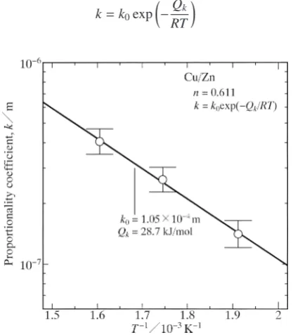
As shown in Fig. 7, n is rather insensitive to T. If n is con-sidered to be independent of T, k and n in eq. (3) are simulta-neously evaluated by the least-squares method from all the experimental points plotted in Fig. 3. The evaluated value of n is shown as a solid circle with error bars in Fig. 7, and those of k are indicated as open circles with error bars in Fig. 9. In Fig. 9, the ordinate shows the logarithm of k, and the abscissa indicates the reciprocal of T. The dependence of k on T is
generally expressed by the following equation.30)
k=k0exp −RTQk (8)
Here, k0 is the pre-exponential factor, and Qk is the activation enthalpy. From the open circles in Fig. 9, k0 and Qk were eval-uated by the least-squares method as shown with a solid line. The evaluated values are indicated in Fig. 9. If the layer growth is purely controlled by volume diffusion with n = 0.5, the dependence of k on T is estimated from the interdiffusion coefficients and the solubility ranges of the constituent phases in the diffusion couple by an appropriate analytical
tech-nique.12–22) On the basis of the estimation, Qk is compared
with the activation enthalpy of the interdiffusion coefficient for each phase. However, n is greater than 0.5 as shown in
Fig. 7. Hence, unfortunately, the analytical technique12–22)
cannot be used to estimate the value of Qk in a straightforward manner. The rate-controlling process of the layer growth is
usually discussed on the value of Qk. As mentioned earlier,
however, the layer growth at T = 523–623 K is controlled by volume diffusion and interface reaction. Therefore, Qk con-tains mixed-information on the temperature dependencies of volume diffusion and interface reaction. In such a case, the rate-controlling process cannot be estimated only from the value of Qk. It is worth noting that n is much more useful than Qk for the estimation of the rate-controlling process.
4. Conclusions
The solid-state reactive diffusion in the Cu/Zn system was experimentally observed using the Zn/Cu/Zn diffusion cou-ples prepared by the diffusion bonding technique. The diffu-sion couples were isothermally annealed at temperatures of T = 523, 573 and 623 K for various times up to t = 49 h. During annealing, the γ + ε two-phase layer forms at the orig-inal Cu/Zn interface in the diffusion couple, where the thick-ness is smaller for the ε layer than for the γ layer. The total thickness of the two-phase layer is proportional to a power function of the annealing time. The exponent of the power function takes intermediate values between 0.5 and unity un-der the present annealing conditions. This means that both volume diffusion and interface reaction contribute to the rate-controlling process of the layer growth.
Acknowledgements
The present study was supported by the Iketani Science and Technology Foundation in Japan. The study was also par-tially supported by a Grant-in-Aid for Scientific Research from the Ministry of Education, Culture, Sports, Science and Technology of Japan.
REFERENCES
1) T.B. Massalski, H. Okamoto, P.R. Subramanian and L. Kacprzak:
Bina-ry Alloy Phase Diagrams, vol. 3 (ASM International, Materials Park, OH, 1990) p. 3417.
2) K. Suganuma and K. Niihara: J. Mater. Res. 13 (1998) 2859–2865.
3) S.-P. Yu, H.-J. Lin, M.-H. Hon and M.-C. Wang: J. Mater. Sci.: Mater. Electron. 11 (2000) 461–471.
4) I. Shohji, T. Nakamura, F. Mori and S. Fujiuchi: Mater. Trans. 43 (2002) 1797–1801.
5) M. Date and K.N. Tu: J. Mater. Res. 19 (2004) 2887–2896.
6) M.N. Islam, Y.C. Chan, M.J. Rizvi and W. Jillek: J. Alloy. Compd. 400 (2005) 136–144.
7) J.-W. Yoon and S.-B. Jung: J. Mater. Res. 21 (2006) 1590–1599.
[image:6.595.65.279.533.772.2]8) K. Suganuma and K.-S. Kim: J. Mater. Sci.: Mater. Electron. 18 (2007) 121–127.
9) T. Takenaka, S. Kano, M. Kajihara, N. Kurokawa and K. Sakamoto:
Mater. Sci. Eng. A 396 (2005) 115–123.
10) A. Hoxha, H. Oettel and D. Heger: Proc. 7th Int. Conf. Balkan Phys. Union, Alexandroupolis, (America Inst. Phys., 2009) pp. 591–595. 11) T.B. Massalski, H. Okamoto, P.R. Subramanian and L. Kacprzak:
Bina-ry Alloy Phase Diagrams, vol. 2 (ASM International, Materials Park, OH, 1990) p. 1509.
12) M. Kajihara: Acta Mater. 52 (2004) 1193–1200.
13) M. Kajihara: Mater. Sci. Eng. A 403 (2005) 234–240.
14) M. Kajihara: Mater. Trans. 46 (2005) 2142–2149.
15) M. Kajihara: Diffus. Defect Forum 249 (2006) 91–96.
16) M. Kajihara: Mater. Trans. 47 (2006) 1480–1484.
17) Y. Tanaka and M. Kajihara: Mater. Trans. 47 (2006) 2480–2488.
18) M. Kajihara and T. Yamashina: J. Mater. Sci. 42 (2007) 2432–2442.
19) M. Kajihara: Mater. Trans. 49 (2008) 715–722.
20) M. Kajihara: J. Mater. Sci. 44 (2009) 2109–2118.
21) M. Kajihara: Mater. Trans. 51 (2010) 1242–1248.
22) M. Kajihara: Mater. Trans. 53 (2012) 1896–1904.
23) Y. Muranishi and M. Kajihara: Mater. Sci. Eng. A 404 (2005) 33–41.
24) T. Hayase and M. Kajihara: Mater. Sci. Eng. A 433 (2006) 83–89.
25) K. Mikami and M. Kajihara: J. Mater. Sci. 42 (2007) 8178–8188.
26) M. Kajihara and Y. Tejima: J. Phys.: Conf. Ser. 165 (2009) 012091. 27) Y. Tejima, S. Nakamura and M. Kajihara: J. Mater. Sci. 45 (2010) 919–
928.
28) M. O, Y. Takamatsu and M. Kajihara: Mater. Trans. 55 (2014) 1058– 1064.
29) T. Heumann: Diffusion in Metallen, (Springer-Verlag, Berlin, 1992) p. 30.
30) T. Yamada, K. Miura, M. Kajihara, N. Kurokawa and K. Sakamoto: