A LINEAR DIODE ARRAY FOR ASTRONOMICAL SPECTROSCOPY
A thesis
submitted in partial fulfilment of the requirements for the Degree
of
Doctor of Philosophy at the
University of Canterbury by
Phillip
J.
MacQueenTHESIS
I
CHAPTER
1
TITLE PAGE
DEDICATION
TABLE OF CONTENTS
LIST OF FIGURES
LIST OF PLATES
LIST OF TABLES
GLOSSARY
LOGIC WAVEFORMS
SYMBOLS
ABSTRACT
IN1RODUCTION
rnARACTERISfiCS OF SOLID-SfA1E DETECTORS
1.1 Photometric Transfer Functions
1.1.1 Two-parameter Linear Fuctions
1.1.2 Photometric Non-lineraity
1.2 Detector Output Noise
1.2.1 The Signal-to-noise Ratio
1.2.2 Noise Characteristics and Sources
1.2.3 Transfer Fuction Augmented Noise
1.2.4 The Detector Noise Domains
1.3 Dynamic Range
1.4 Detector Efficiency
1.4.1 Signal-to-noise Efficiency
1.4.2 Responsive Quantum Efficiency
1.4.3 Detective Quantum Efficiency
PAGE
i
ii
iii
X
xviii
xix
XX
xxi
xxii
1
3 7 8 8
9
10 10 10 11
14
2
3
THE LDA DETECfOR
2.1 Electronic Response and Parameters 2.1.1 The p-n Junction
2.1.2 The Integrating Photo-diode Sensor 2.1.3 Physical Organization and Operation 2.1.4 The LDA Circuit Representation 2.1.5 The Fixed Pattern
2.1.6 Intrinsic LDA Noise Sources a) Thermodynamic Reset Noise b) Fixed Pattern Noise
c) Net Intrinsic Detector Noise
2.2 Readout Techniques
2.2.1 Video Voltage Level Processing
a) Reset Switch Action
b) Readout Operation and Response c) Linearity
2.2.2 Recharge Current Processing a) Readout Operation
b) Performance and Stability 2.2.3 Readout Technique Comparison 2.3 Performance Characteristics
2.3.1 Responsive Quantum Efficiency 2.3.2 Modulation Transfer Fuction 2.3.3 Thermal Leakage Current 2.3.4 Blooming and Image Lag 2.3.5 Cosmic Ray Sensitivity 2.4 Operation Requirements
ELEcrROMEaiANICAL DESIGN
3.1 Electromagnetic Compatability
3.1.1 Electromagnetic Interference a) Common-impedance Coupling b) Electric-field Coupling c) Magnetic-field Coupling d) Methods of Controlling EMI 3.1.2 Grounding and Shielding
4
3.2 The MJUO LDA Electromechanical Design 3.2.1 Required Electronic Functions 3.2.2 Earth Connections
3.2.3 The Electronics Distribution
3.2.4 General Electronic Hardware Implementation a) Printed Circuit Boards
b) Active Components c) Passive Components 3.3 The Interface Chassis
3.3.1 The Power Supplies
a) Utility Power Conditioning b) The Transformers
c) Pre-regulation Power Supplies d) Power Supply Fault Detection e) Dewar Power Supply Regulation f) The Hardware Implementation 3.3.2 Control Signal Distribution
a) Differential Logic Transmission
b) The Grounding, Shielding, and Circuitry c) The Hardware Implementation
3.4 The LDA Interface and Acquisition Rack
THE CRYOGENIC DETECTOR HEAD 4.1 The Mechanical Sub-systems
4.1.1 The Dewar Tank
a) The Cryogen Storage Tank b) The Thermal Link
c) Thermal Insulation d) The Vacuum and Cryopump 4.1.2 The Dewar Lid
a) The Rotation Mechanism b) Light Trap
c) Optical Window
4.1.3 The Electronics Assembly a) The Diode-array Mounting b) The Mounting Flange
c) The Co-axial Feedthroughs d) The Electronics Boxes 4.1.4 The Cryogenic Performance
a) Thermal Leakage
b) Thermal Time Constants
c) The Natural Temperature Dependance
5
4.2 The Temperature Controller
4.2.1 The Servo-loop Principle
a) Servo-loop Theory
b) Amplifier Types
4.2.2 Physical Realization
a) The Temperature Sensor
1) The Implementation
2) Physical Parameters
3) Noise Analysis b) Servo-loop Design
1) Theory of Stability Analysis
2) Servo Loop Parameters c) The Electronic Circuitry
1) The Heater
2) The Amplifier Gain
3) The Amplifier Circuit Diagram 4) The Printed Circuit Board
4.2.3 Performance 4.3 The Thermometers
4.3.1 The Block Thermometer
4.3.2 The Ambient Theromoeter
VIDEO PROCESSING
5.1 General Design Requirements
5.1.1 Performance
5.1.2 Operating Frequency and Hardware
5.2 Diode Array Bias Supply
5.2.1 Requirements
5.2.2 The Circuitry and Implementation
5.2.3 Performance
5.3 Video Amplification
5.3.1 Video Processing Gain
5.3.2 Preamplification a) Requirements
1) Amplification 2) Amplifier Noise
3) Bias Current Deleterious Effects
b) Existing Design
c) The Pre-amplifier Circuit Design
d) Hardware Implementation
6
5.3.3 Variable Amplification
a) Requirements
b) Circuitry
c) Hardware Implementation
5.4 Video Signal Extraction and Noise Rejection
5.4.1 Correlated Double Sampling
a) Signal Extraction
b) Thermodynamic Noise Rejection
c) Noise Filtering Response
5.4.2 Bandwidth Limiting
a) Resetable Integrator
b) Bessel 3-pole Low-pass Filter
5.4.3 Video Processing Transfer Function
5.4.4 Reset Switch Action
a) Video Current Noise Source
5.5 Video Processing Circuitry and Hardware
5.6 Analogue-to-digital Conversion
5.6.1 Requirements
5.6.2 Electronic Circuits and Operation
5.6.3 Conversion Timing
5.6.4 Hardware Implementation
DIODE ARRAY CONTROLLING
6.1 Requirements
6.1.1 Reset Switch Control Logic
6.1.2 Clocks and Start Pulse Logic
6.2 Electronic Circuits
6.2.1 Precision Power Supplies
6.2.2 Reset Switch Drivers
6.2.3 The Start Pulse Logic
6.2.4 The Clock Drivers
6.3 Hardware Implementation
6.4 Performance ane Operating Parameters
7
DATA
A~UISITIONAND REDUCfiON
7.1 The Data Acquisition System
7.1.1 The Microprocessor Chassis a) The Hardware Organization b) The CPU and Memory
c) The Peripheral Interfaces 7.1.2 The Peripherals
a) The Terminal b) The Disk Drives
c) The Printer and Plotter 7.1.3 The Detector Interface
a) Requirements
b) Hardware Implementation c) Software Implementation 7.1.4 The Disk Operating System 7.2 The LDA Control Programme
7.2.1 The Software Environment a) User Interaction
b) The Runtime Environment c) The Image Frames
7.2.2 Detector Control Software a) Readout Software
b) Auxiliary Hardware Control c) Testing Support Routines 7.2.3 Data Reduction
a) Fixed Pattern Subtraction b) Base Line Subtraction c) Flat field Division d) Deglitching
e) Fast Fourier Filtering f) Dispersion Solution Fitting 7.2.4 Data Display
7.2.5 Disk File Operations
8
9
HR4492: A S0UTIIERN RS CVn BINARY
8.1 Introduction
8.2 Observations
8.3 Analysis
8.3.1 Radial Velocities
8.3.2
Ha
Line Profile Variability8.3.3 The April 1986
Ha
Spectra8.3.4 Helium and Lithium Observations
8.4 Discussion
SUMMARY AND FUilJRE WORK
9.1 Summary 9.2 Future Work
9.2.1 Characteristics and Calibration
9.2.2 Detector Operation
9.2.3 Data Reduction
ACKNOWLEDGEMENTS
REFERENCES
APPENDICES
1 Operational Amplifiers
2 Thermal Noise
3 Low Frequency Noise
4 Addition of Noise Voltages
5 Temperature Coefficient Results
6 The Reticon RL Series Specification Sheet
7 The Burr-Brown OPA102BM Operational Amplifier
8 The AMD Am9513 System Timing Controllers
9 The Terminal Custom Character Sets
10 The LDA Mounting Block
11 The Preamplifier Printed Circuit Boards
12 The Dewar Flange Plate
13 Programme BSY38NSE Listing
14 Programme TC_sTP_R Listing
221
221
224
225
225
229
233
236
238
241
241
242
243 244
245
246
LIST OF FIGURES
FIGURE
PAGE
1.1 Plot showing (a) the best linear fit to the detector response, and (b) the non-linear error function for this response.
2.1 Schematic representation of the structure of the Reticon RLxxxxF/30 series photo-diode array.
2.2 Circuit representation of a shift register.
2.3 Time-varying waveforms (clocks, ~1 and ~2 • and the start pulse) for the shift registers.
2.4 Equivalent electronic circuit for a self-scanning photo-diode array.
2.5 High input impedance amplifier conditioning the video signal.
2.6 Equivalent circuits for initialization of (a) diode capacitance, Cd' and
(b) video capacitance, C . v
2.7 Schematic representation of the control signal timing, the reset switch action, and a typical video voltage output at readout.
2.8 Low input impedance current-to-voltage amplifier interfacing a video line to the external signal processing.
2.9 Schematic representation of the control signal
2.10
timing for recharge current processing, and the resulting output signal.
RQE for a Reticon RL1024S as a function of wavelength for T=0°C.
9
20
21
21
22
26
26
29
30
FIGURE
2.11
2.12
2.13
3.1
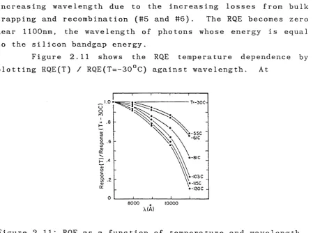
RQE as a function of temperature and wavelength.
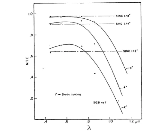
MTF as a function of wavelength for the sampling frequencies shown.
Thermal leakage versus temperature for different linear diode array systems.
General circuit for common-impedance coupling.
3.2 An example of an emitter-type logic circuit producing common-impedance coupling.
3.3 An example of a susceptor-type logic circuit producing common-impedance coupling.
3.4 General circuit for electric-field coupling. (a) The physical representation, and
(b) its equivalent circuit.
3.5 Electric-field coupling configurations in the (a) low, and {b) high frequency limit.
3.6 General circuit for magnetic-field coupling. (a) The physical representation, and
{b) its equivalent circuit.
3.7 A simple, but important example of magnetic-field
3.8 3.9 3.10
coupling.
A single-ended amplifier.
A differential amplifier.
The (a) physical representation, and equivalent circuit for determining of a differential amplifier with a impedance imbalance.
(b)
the EMI source
PAGE
35
36
37
42
43
43
44
45
46
47 49 49
FIGURE
3.11 The (a) physical representation, and (b)
equivalent circuit of a source and
single-ended amplifier with an undesirable connection
PAGE
to the external ground. 51
3.12
3.13
3.14
3.15
3.16
3.17
3.18
3.19
3.20
3.21
The (a) physical representation, and (b) equivalent circuit of an amplifier shield not connected to the electrostatically shielded circuitry.
Two physical representations showing possible connections of the electrostatic shield to the signal ground.
The physical representation of a correctly
applied electrostatic shield to a differential amplifier.
A coil depicted as a capacitance connected to the grounded, electrostatic shield.
The two examples of ground-shield connections for a single-shielded transformer.
Ground-shield conections for a double-shielded transformer.
Ground-shield connections for a triple-shielded transformer.
The effectiveness of magnetic shielding.
Schematic representation of the sub-systems of the MJUO LDA system.
Schematic representation of the grounding, shielding, and distribution of tasks within the MJUO LDA dewar.
52
53
54
55
55
56
56
59
62
FIGURE
3.22
3.23
3.24
3.25
The (a) positive, and (b) negative power supply filters for an operational amplifier.
The printed circuit board layout of an operational amplifier, and its power supply filters.
Electronic circuit for a single positive voltage power supply.
Physical layout of the primary coil, and the
PAGE
68
69
73
four secondary coils on the transformer core. 77
3.26
3.27
3.28
3.29
3.30
3.31
4.1
4.2
Schematic representation of one of the secondary coils.
Printed circuit board layout for a pre-regulator circuit.
Differential distribution of logic signals down a transmission line.
Electromagnetic coupling behaviour along a transmission line.
Control signal distribution electronic circuit.
Printed circuit board layout for control signal interface electronics.
Composite cross-section of the MJUO LDA dewar.
Thermal circuit diagram which is used for
determining the diode array block temperature.
4.3 Rate of change of cryogen mass which is used for determining the power dissipation by the
cryogen.
77
88
90
91 92
94
100
101
FIGURE PAGE
4.4 Typical cooling curve for the MJUO dewar. 113
4.5 Block diagram for a servo-loop controller. 116
4.6 Controller power and block transfer curves as a
function of temperature. 119
4.7 Block diagram showing the addition of the
derivative of the servo-loop error signal to
that signal. 120
4.8 Circuit representation of a differentiating amplifier.
4.9 Temperature sensor electronic circuit with the
4. 10
4.11
4. 12
4. 13
4.14
4.15
4.16
5. 1
5.2
precision voltage reference circuit.
Response of a BSY 38 transistor, the temperature sensor, to immersion in liquid nitrogen.
Block diagram showing the components of noise in the temperature sensor circuit.
Response of the temperature controlling circuitry to a step input.
Temperature controller electronic circuit.
Reference temperature electronic circuit.
Block thermometer electronic circuit.
Ambient thermometer electronic circuit.
Electronic circuit for the LDA bias supply.
The video processing noise model.
121
122
124
125
131
134
136
138
139
144
FIGURE
5.3 Preamplifier electronic circuit.
5.4 Printed circuit board for the preamplifier electronics given in figure 5.3
5.5 Cross-section of the cold block, showing the LDA mounted in its sockets.
5.6 Video offset reference (VOR) voltage circuit.
5.7 Video processing electronic circuit.
5.8 Printed circuit board layout for video processing electronics.
5.9 Response of the low-pass filter to the maximum
5.10
video reset step.
The transfer function of the video processing electronics, and the response of the low-pass
PAGE
156
160
161
163
164
167
171
filter. 172
5.11
5.12
5.13
5.14
5.15
Electronic circuit showing the multiplexing of the four differential video lines.
Difference amplifier common-mode rejection ratio (CMRR) as a function of the data rate frequency.
Electronic circuit for the
AID
convertor, including its signal acquisition and data serialization.Control waveforms for the
AID
and data serialization processes.Printed circuit board layout for A/D conversion and temperature controlling electronics.
174
175
178
180
FIGURE PAGE
5.16 Noise Gaussian for the {a) low, and (b) high
impedance cases of a noiseless signal source. 184
5.17 Noise Gaussians with the LDA under operating
conditions.
6.1 Electronic circuit for the precision voltage
reference.
6.2 Electronic circuit for a negative power supply
used by the clock electronics.
6.3 Electronic circuit for a positive power supply
used by the clock electronics.
6.4
Electronic circuit used to drive reset switches.6.5 Electronic circuit used for conditioning the
6.6
6.7
6.8
start pulse control signal.
Electronic circuit used for producing clock
waveforms
f
1 andf
2 •Waveforms generated at the nodes showm in
figure 6.6.
Electronic circuit used to condition each clock.
6.9 Printed circuit board layout for the reset and
7.1
7.2
7.3
control logic conditioning.
Waveforms, as generated by the STCs, for
controlling the MJUO LDA.
Software storage format for image frames.
Unfiltered power spectrum.
185
188
188
189
189
190
191
191
192
195
206
211
FIGURE
PAGE
7.4 Sample plotter output - HR4492
Ha
spectrum. 2187.5 Display format for an image frame header. 219
8.1 Radial velocity versus Julian Date, showing the
precision of the velocity determination. 227
8.2 Radial velocity versus phase, using the ephemeris
given in eq. 8.2 (from Collier 1982}. 227
8.3 As for figure 8.2, except using the new ephemeris. 228
8.4 Temporal sequence of Ha-region absorption spectra. 230
8.5 Temporal sequence of residual spectra,
corresponding to spectra given in figure 8.4. 231
8.6 Temporal sequence of three residual spectra, and
their corresponding spectra, at a similar phase
to those shown in figures 8.4 and 8.5.
8.7 Two
Ha
image tube spectra at similar phases asthe digital spectra.
8.8 Two temporal sequences, at similar phases but on
successive cycles, of residual spectra showing
the
Ha
emission and absorption profiles.8.9 Possible
Ha
spectrum (at ~=0.08) of HD101380, the8.10
visual companion of HR4492.
A sample of HR4492 spectra showing regions
around A~5876A {D3 ) , A~4686A (Hell). and
A~6707A (Li I).
232
234
235
236
LIST OF PLATES
PLATE
3.1 A general view of an interface chassis.
3.2 An isolated line driver board and triple-shielded transformer.
3.3 Stages in shielding a transformer primary coil.
3.4
Stages in shielding a transformer secondary coil.3.5 Internal view of a utility power conditioning box.
3.6 Three views of the pre-regulated power supplies.
3.7 Front view of the LDA Data Acquisition System and Interface rack.
3.8 Rear view of the LDA Data Acquisition System and Interface rack.
4.1 The MJUO linear diode array dewar.
5.1 The LDA preamplifier board and cold block.
5.2
The video processing printed circuit board.5.3 The A/D conversion and temperature controlling printed circuit board.
PAGE
71
74
79
80
87
89
96
97
99
159
165
181
6.1 The diode array controller board. 194
7.1 The Data Acquisition System microprocessor chassis. 198
7.2 General operating format of the LDA programme. 208
7.3 Interactive graphics display format of the LDA
LIST OF TABLES
TABLE
3.1 Effectiveness of shielding materials.
3.2 Rectifying and smoothing circuitry parameters for
a peak capacitor voltage of 14.5 V in the 5 V
power supplies.
3.3 Rectifying and smoothing circuitry parameters for
a peak capacitor voltage of 24.5
V
in the ±15V
power supplies.
5.1 Amplifier fractional gain error as a function of
open to closed loop gain ratio.
7.1 Waveforms generated by the counters of each STC.
8. 1 Existing
Ha
spectroscopic observations of HR4492.8.2
LDA
spectroscopic observations of HR4492.8.3 Spectral lines used for radial velocities.
PAGE
58
83
83
150
205
223
224
ac A/D CMOS CPU de e-/h EMC EMI EPROM DOS DQE JFET kbyte LDA LSB MJUO MOSFET MTF PCB ppm RAM r.m.s. rti RQE STC swg TC UCPD GLOSSARY
alternating current (or non-zero frequencies)
Analogue to Digital Convertor
Complementary Metal Oxide Semiconductor
Central Processing Unit
direct current (or zero frequency component)
electron/hole
Electromagnetic Compatability
Electromagnetic Interferrence
Erasable/Programmable Read Only Memory
Disk Operating System
Detective Quantum Efficiency
Junction Field Effect Transistor
1024 bytes
Linear Diode Array
Least Significant Bit
Mount John University Observatory
Metal Oxide Semiconductor Field Effect Transistor
Modulation Transfer Function
Printed Circuit Board
parts per million
Random Access Memory
root mean square
referred to input
Responsive Quantum Efficiency
System Timing Controller
standard wire gauge
Temperature Coefficient
LOGIC WAVEFORMS
E Logic waveform 'Example' which causes its action when 'high'.
E
Logic waveform 'Example' which causes its action when 'low'.E
Logic waveform 'Example' which causes its action ewith a positive going edge.
E
Logic waveform 'Example' which causes its action ewith a negative going edge.
C Master Clock for the shift register which reads out the
0
c
e$1
$2
s
eREV
SHR
SHP
A1
A2
ADC - - e PL DAVsc
e
odd numbered pairs of diodes.
First clock for the odd shift register. Second clock for the odd shift register. Start pulse for the odd shift register. Reset Odd Video
Master Clock for the shift register which reads out the even numbered pairs of diodes.
First clock for the even shift register. Second clock for the even shift register. Start pulse for the even shift register. Reset Even Video
Sample when high, and Hold when low the Reset video level for the odd shift register. (Named SHP for the even shift register.)
Sample when high, and Hold when low the Pixel level for the even shift register. (Named SHR for the odd
shift register)
Video Multiplexer address line 1. Video Multiplexer address line 2.
A/D convertor input multiplexer Address line 1. A/D convertor input multiplexer Address line 2.
Analogue to Digital Convert.
Parallel Load the A/D data into the shift register. Data AVailable to the Data Acquisition System.
SYMBOLS
Circuit Diagram Symbols:
- D
Signal input to circuitSignal output from circuit
Qi---0 Continuation of signal distribution
GP Ground Plane
Zero signal reference (Signal ground)
Power Earth
Continuation of zero signal reference
Connections to power supply
Resistor
Variable resistance
Capacitor, (optional '+' for polarity)
Variable capacitance
Stray (undesirable) capacitance
Diode
Light emitiing diode
Zener diode
Triac
Metal Oxide Varistor
I
~srI
r--,
ICircuitl L __ ...J
=t>-
w--@
~
-[>-
+-
=D--[tL:
~
v-
-Q-Test point (Oscilloscope probe hook)
Mini-jump option selector
Twisted pair cable
Shielded twisted pair cable
Co-axial cable
Undesirable commom-mode voltage generator
Current noise source
Analogue power supply filter
Internal representation of a component
Operational amplifier (or comparator)
SD214 D-MOS switch
NPN transitor
PNP transitor
Inverting logic gate
Inverting logic gate with input hysterisis
Negated AND (NAND) logic gate
Differential logic line driver
Differential logic line receiver
Quad input active low or gate
$-
LM334 constant current source:~-J.:
Lf-T~
LM339 precision voltage referencer--~
!~-'d_
HP137 optical couplerPrinted Circuit Board Symbols:
0----~
LQJ
D
0
1.0 mm diameter signal path
Wide track for high current paths
Connection of component to PCB GP
Rogers Q/PAC dual strip transmission line
Resistor (or polystyrine capacitor if big)
20 turn variable resistor
Zero ohm jumper
MKT1817 100 nF 63V capacitor
Tantulum capacitor
MKT 1818 (or 1822) Polypropylene capacitor
Variable capacitor
1N4007 diode
~
~
D
~
~
Q
~
0
~
~
Test point (Oscilloscope probe hook)
Plastic or ceramic packaged integrated circuit in socket. Free 'dots' indicate pins connected to ground plane, circled dots indicate unconnected pins.
T099 metal can packaged integrated circuit in socket.
Medium power transistor
LM339 precision voltage reference
SD214 D-MOS switch
LM134 constant current source
LM185-2.5 volt zener reference diode
Connhex 50 Q co-ax receptacle
Diode bridge (3 A per leg)
Fuseable link in holder
T0-220 packaged 3-terminal regulator or triac
Right-angle Molex connector (3-pin examale)
ABSTRACT
Future spectroscopic observational programmes at Mount John University Observatory require the ability to acquire spectra with significantly higher spectrophotometric accuracy and geometrical stability than can currently be achieved. Therefore a solid-state linear-diode-array image detector system has been designed and developed for use with the MJUO echelle spectrograph.
A review of those electromechanical design techniques of significance to astronomical instrumentation is presented. Their application is exemplified with a complete electromechanical design for the detector, which is found to allow each electronic sub-system implemented within that design to achieve its theoretical level of performance.
The requirements for the video processing electronics of a solid-state image detector are explicitly developed, and are used to design the electronics for this detector. Subtle sources of electronic instability which can appear as noise or base-line shifts are identified and controlled in this design. In particular, differential non-linearity is identified in an existing preamplifier design, and so an alternative design is implemented.
The readout noise of the entire detector system is measured to be 200 e-/h pairs for a noiseless signal source of zero impedance to ground. This increases to 350 e- /h pairs when the impedance of this source is equal to that of the diode array, due to an additional noise contribution of 290 e-/h pairs. The net readout noise with the RL936F/30 diode array is 450 e-/h pairs, which is the quadratic sum of the detector system noise with the two 210 e-/h pair samples of diode capacitance thermodynamic noise. Thus the diode array is not found to contribute any noise in excess of its theoretical thermodynamic noise.
is ±20 mK, which is dependent on the design of the dewar.
The hardware and software which provide interactive instrument control and data reduction are described. In particular, they provide for flexible control of the detector sub-systems during data acquisition and testing, and enable a high level of data reduction to be undertaken while the detector is integrating.
INTRODUCTION
For an overall understanding of the chemical and dynamical evolution of our Galaxy, the physical and chemical properties of its components have to be deduced. This may involve a wide range of observational work (for example, on the interstellar medium or individual stars in both the disk and halo populations), laboratory work (for example, on line oscillator strengths or chemical reaction rates), and theoretical work (for example, stellar structure and evolution). As part of the observational work, there are many astrophysically interesting research areas (for example isotopic ratios, stellar radial velocities, and line profile analysis), which require the use of detectors capable of obtaining data with signal-to-noise ratios significantly higher than 100:1, and with correspondingly high spectrophotometric accuracy.
Griffin's (1968) use of photographic plates as a detector has shown that it is extremely difficult to calibrate
their non-linear response to a spectrophotometric precision of better than 1% for even the brightest stars. Therefore during the last decade, a number of research groups have developed solid-state detector systems to address specific astrophysical problems which require higher signal-to-noise ratios and spectrophotometric accuracies than can be achieved by photographic plates.
The McDonald Observatory system (Vogt, Tull, and Kelton 1978) has been used extensively by Lambert and his colleagues for stellar atmosphere analysis using weak line equivalent widths (see for example, Sneden et al. 1981, and Dominy et al. 1978), and for identifying the secondaries of spectroscopic binaries (see Tomkin 1978). High quality data obtained with a similar system at the European Southern Observatory coude auxiliary-feed telescope, has, for example, been used by Federman et al. (1984) to observe weak interstellar features, and by Lambert and Danks (1985) to observe the weak helium D3
source. Gray (1982a,b) has extensively analysed line profiles in stellar spectra to obtain their rotation and turbulence information, and thereby identify a dynamo rotational braking mechanism in stellar evolution. Additional line profile data from his system at the University of Ontario (Gray, 1986) are leading to an understanding of the turbulent motions within stellar atmospheres. Vogt (1982) has developed a system at Lick Observatory which he has applied to Doppler imaging of starspots in chromospherically active stars (see Vogt and Penrod 1983). Finally, Campbell et al. (1979, 1981} has introduced an hydrogen-fluoride cell into his optical path in an effort to measure radial velocities with the extremely high precision of ~10 ms-1 In common with the work of Gray is the demonstration of high geometrical stability in their systems.
Of astronomy
Indeed,
revolutionary significance are the various solid-state the above examples have been
sensor.
to observational image detectors. undertaken using a While this thesis self-scanning linear
will concentrate on
diode-array
this type of detecting element, a discussion of other types of solid-state detectors used in astronomy is given by Timothy (1983), and in references
therein.
This thesis is organized to give the reader a thorough development of the total concept involved in the design, construction, and use of a Linear Diode Array detector for high resolution stellar spectroscopy.
In order to discuss any solid-state detector system, the terminology and basic definitions required need to be introduced. These will be given in Chapter 1, and will include the response of the detector to illumination, its sources of noise, its dynamic range, and its efficiency. The linear diode array detector will be described in Chapter 2. In particular, details of its operating environment, and the method by which data is retrieved from the detector are given. In addition, the basic ideas raised in Chapter 1 are specifically addressed in relation to the linear diode array. Most of the material in these two chapters has been developed
Having selected a detector, the rest of the instrument package must be designed to produce an integrated physical system. In Chapter 3, the requirements for the underlying electromechanical design of that system are determined, and the techniques for achieving them are reviewed. Specific details of its implementation in the Mount John University Observatory LDA system are given there, and also in Chapter 4. This latter chapter also deals with the cryogenics, as well as
the justification for, and the means by which the temperature environment is controlled.
Chapters 5 and 6 determine the requirements and designs the electronic sub-systems which process the video signal and control the array. Given their implementation within the electromechanical design, this process need only consider the circuitry requirements of those electronics. Careful attention to detail enables many subtle sources of noise and instability to be identified and minimized.
The acquistion and reduction of the digital data, for which this whole system was designed and intended, is outlined in Chapter 7. It gives a description of the Data Acquisition System hardware, and of the software options which are available for performing these tasks.
Finally, the ultimate proof of the performance of any system is how i t performs on the astronomical instrument and in the working environment for which i t was intended. In spite of electrostatic discharge damage that existed in the diode array chip for this system, a number of moderate quality spectra of the chromospherically active HR4492 system are able to be given in Chapter 8. They are used to derive a new orbital period and ephemeris for HR4492, as well as to detect both the helium D3 and Li I 6707A features. Variations in the
line profile of Ha are reduced from the spectra, and are interpreted in terms of possible mass transfer within the system.
The electronic and geometrical stability of this instrument will allow many new astrophysical problems to be carried out at Mount John University Observatory. They will include weak
monitoring of stars, and velocities.
CHAPTER ONE
CHARACTERISTICS OF SOLID-STATE DETECTORS
An astronomical instrument is optically configured so that it collects the quanta of electromagnetic radiation from its target, and images them onto its image detector in a desired representation. The image detector is a device that captures photons that are incident upon it, and converts them into a recordable form. The desirable properties of this detector include the following.
1) A large portion of the image produced by the optical configuration of the instrument can be imaged onto it.
2) It converts a high proportion of the photons that are imaged onto it into recordable form.
3) It operates over a large range of photon arrival rates. 4) The incident image is reliably and precisely calculable from the recorded signal.
5) It is operationally simple, reliable, and robust.
Of revolutionary significance to observational astronomy is the solid-state group of image detectors.
A solid-state image detector collects photons from the spatial pattern of illumination incident upon its surface, and converts them into a voltage waveform which is a discretely sampled, ordered, sequential representation of the incident radiation pattern. The collection process is referred to as an integration, the voltage waveform is referred to as a video signal, and the discrete samples in the waveform correspond to individual picture elements called pixels. The mechanism for producing the time-varying video signal is referred to as scanning, and the scanning function is accomplished by the application of one or more electrical signals
the ordered sampling of the pixels. The converting the video signal into recordable represent the number of photons detected by called video processing. The resulting array
which produce technique of numbers, which each pixel, is of numbers is referred to as a frame,
those numbers will be
a readout, and that event signifies the end of the integration interval for that frame.
1.1 Photometric Transfer Functions
The photometric transfer function of a specified pixel is that function which specifies the recorded signal of the pixel for a given input illuminance. If the transfer function is the same for all pixels, i t is said to be homogeneous over the detector format.
A
transfer function is said to be homologous over the detector format if it has the samefunctional form for all pixels.
1.1.1 Two-parameter Linear Functions
It is scarcely to be hoped that a detector system with more than one pixel can have a homogeneous transfer function, but a multi-pixel system can realistically be specified to have a homologous transfer function. This is truly desirable as the procedures for determining the transfer function and for performing the corresponding photometric correction separately for every pixel in the format could be formidable. The most desirable homologous pixel transfer function has a linear two-parameter functional form; one additive parameter representing the photometric zero point of the pixel, and one multiplicative parameter specifying the relative photometric sensitivity of the pixel. Equation 1.1 expresses this for detector pixel
zero point FP.,
1
t i ' in terms of
for a response
R.
1the as R.
=
S.FF. + FP.1 1 1 1
signal
s.
1 gain FF., 1 and
( 1. 1)
The response of the detector to the absence of any signal (S. = 0, for all i) is called the fixed pattern, and gives the
1
zero point of every pixel. Therefore if the fixed pattern is subtracted from the response of the detector to uniform illumination (S. =constant, for all i), the resulting frame
1
pattern of relative intensities by subtracting the fixed pattern and then dividing by the flat field.
1.1.2 Photometric Non-Linearity
It is normally considered a performance irregularity if the fixed-patterned response is not linearly related to the input signal. Small deviations from linearity can be easily corrected if the system transfer function is homologous over the detector format, and has the following functional form
R.
=
S. FF. + NL(R.-FP.) + FP.1 1 1 1 1 1 ( 1. 2)
The error function NL(R.-FP.) has in general a non-linear
1 1
dependence on the fixed-patterned signal level, and is assumed to be homogeneous over the detector format. As illustrated in figure 1.1, it can be determined from a plot of the fixed-patterned response versus signal level by fitting a linear curve with the smallest peak-to-peak deviation from the data.
(b)
Figure 1.1: Plot showing (a) the best linear fit to the
detector response, and (b) the non-linear error function for this response.
The fitted curve is assumed to be the linear term S.FF., and 1 1
1.2 Detector Output Noise
Any random representation of noise.
fluctuation causing uncertainty an input signal by a de tee tor is
in the called
1.2.1 The Signal-to-noise Ratio
The precision with which the signal recorded by a detector can represent the actual signal of the illumination pattern is dependent on the net noise, and is quantified as the quotient of the recorded signal level and the noise level, called the signal-to-noise ratio. The signal-to-noise ratio can be specified for the signal from an individual pixel, or to the amplitude of an image feature spread over many pixels. An alternative interpretation of the signal-to-noise ratio is
that it specifies the information content of the signal under analysis.
1.2.2 Noise Characteristics and Sources
The probability distribution of noise amplitudes is described by Poisson statistics because
of the quantum events causing noise. classical systems, the number of events noise is so large that the skewness Poisson distribution is
amplitude probabilities
negligible. can be well
of the random nature However in describing causing the observed and kurtosis of the Therefore the noise approximated by a continuous Gaussian distribution with the same variance as the underlying Poisson distribution.
If the net noise of a system is contributed to by more than one mechanism, it is well known that the instantaneous noise is the sum of the noise amplitudes of the individual mechanisms. Also, the amplitude distribution of the net noise is the convolution of the noise distributions of the individual mechanisms. As the convolution of N Gaussians with standard deviations a.(i=l. .N) is also a Gaussian, the net
1
[
N 2]0.5
a
=
l
aii=1
( 1. 3)
where the a. are the individual mechanism standard deviations.
1
The sources of noise contributing to the net output noise of each detector pixel can be grouped into the following
three categories.
1) Optical signal noise: the detected optical randomly arriving photons has a noise standard
signal of N p deviation of
~N photons according to classical Poisson statistics. This p
signal is the sum of the source and background signals in the general case, and the noise mechanism is referred to as shot noise.
2) Dark signal noise: signal that is detected in the absence of an optical signal is called the dark signal, and has an electronic origin within the sensor. If the dark signal amplitude is equivalent to Nd detected photons, the shot noise of this signal is ~Nd photons.
3) Readout noise: the uncertainty with which the scanning and video processing electronics can measure the signal is called the readout noise. Its standard deviation is expressed as an equivalent number of photons, ar, and is independent of
the signal level.
Therefore the net readout frame noise of a pixel with readout noise a , that
r
dark equivalent photons,
collected Np signal photons, and Nd is found from equation 1.3 to be
( 1. 4) The photometric transfer function must be applied to this
frame to determine the image frame.
1.2.3 Transfer Fuction Augmented Noise
Fixed pattern frames: The required integration time to acquire a fixed pattern frame could theoretically be zero because there is no photon flux, N = 0, to be integrated.
p
Thus only a negligible dark signal, Nd ~ 0, can be accumulated in the short fixed pattern integration time, and therefore it follows from equation 1.4 that the noise of a single fixed pattern frame is equal to the detector readout noise. However consider a numerically generated frame which is the average of nfp fixed pat tern frames, called an averaged fixed pat tern
frame. The signal component of this frame is unchanged from that of any individual frame, whereas the noise component found by first using equation 1.3 for the sum of the noises, is
afp =
a
r
( 1. 5)
Thus the noise of an averaged fixed pattern frame can be made smaller than the noise of the image readout frame. If the time spent collecting the fixed pattern frames is required to be small compared to the integration time of the image frame, an upper limit is placed on nfp implying a lower limit on the fixed pattern noise.
Fixed-patterned frames: these numerically generated frames are the difference between an image readout frame and an averaged fixed pattern frame. Using equation 1.3 to combine the noise of the two operand frames, the noise of a pixel in a fixed patterned image frame is found to be
0
irf-fp
=
J
a 2(1 + _1_) + N + Nd ( 1. 6)
r nfp p
and therefore the signal-to-noise ratio of the information from that pixel is given by
N
s
pNfpf
=
h2[1
+ _ 1l
+ N + Nd ( 1. 7) nfp pwithin the operand frames are given by equations 1.6 and 1.7 respectively. The probability distribution of a fractional error will have the same functional form as the noise distribution of its signal. It follows that the distribution is Gaussian with a standard deviation equal to the quotient of the noise standard deviation and the signal, and that this standard deviation is the reciprocal of the signal- to-noise ratio of the signal. Thus the fractional uncertainty probability distribution of a quotient frame is the convolution of the operand distributions, and has a standard deviation found by using equation 1.3 of
a
_ _ q _
-s
-q
( 1. 8)
where i and f are the operands, and q refers to the quotient frame. The interpretation of equation 1.8 allows the signal-to-noise ratio of a flat-fielded frame to be found from the signal-to-noise ratios of the image and flat-field frames, respectively S/Ni and S/Nf' as
+
= [
[+J:2
+[+]~2r
5
(1.9)
1.2.4 The Detector Noise Domains
If the dark negligible compared
signal with
generation the signal
rate in a detector is photon detection rate, then equation 1.4 shows that there are two independent noise sources which contribute to the net detector output noise: the readout noise and the photon shot noise. Therefore the net noise of any one frame can be characterized as follows.
Readout noise limited domain: when the detected photon signal of a pixel is negligible by comparison to the square of the readout noise of the pixel, the signal is said to be readout noise limited. In this response domain the noise is independent of the signal level, and thus the signal-to-noise ratio is linearly dependent on the signal level.
Photon noise limited domain: when the square of the readout noise of the pixel is negligible by comparison to the detected photon signal in that pixel, the signal is said to be photon noise limited. In this response domain, both the noise and signal- to-noise ratio are equal to the square-root of the detected photon signal. An additional property of operating in this domain is that the subtraction of the fixed-pattern, in the transfer function correction process, does not contribute to the net output noise.
1.3 Dynamic Range
The dyanamic range of a detector specifies the range of responses to which the detector can respond. Therefore quantifying dynamic range depends on how the response of the detector is defined. For this purpose, the response will be defined to be the response from a single pixel when measured in units of the signal level that corresponds to unit signal-to-noise ratio ( but alternatively see Livingston et al. 1976 ) . For a readout noise limited detector that exhibits a fixed-pattern signal, the dynamic range is therefore the quotient of the maximum possible fixed-patterned signal and the net noise of the detector, as given by
Dynamic Range
=
Maximum fixed-pattern Signal LevelCombined Readout and Dark Noise (1.10) In the general case, the dynamic range of a photon counting detector is also given by equation 1.10 because of the detector dark noise, although both the readout noise and fixed pattern noise will be zero. However from the original definition, the dynamic range of a photon counting detector in the absence of dark noise will be the maximum number of photons that i t can record.
Thus, dynamic range will be thought of as the maximum possible response of the detector relative to the minimum response at which the presence of an optical signal can be detected.
1.4 Detector Efficiency
A detector system can be thought of as an instrument that records the information encoded in an illumination pattern that is incident upon it. The efficiency with which the detector collects that information can be quantified as the fraction of the incident information that can be recorded.
1.4.1 Signal-to-noise Efficiency
1.2.1. Therefore the efficiency with which a detector collects an image is defined to be the fraction of the signal to-noise ratio available in the integrated incident image, that has been recorded by the de tee tor in that integration time. The author refers to this quantity as the Signal-to-Noise Efficiency, SNE, and expresses it as
SNE =
[+]recorded
[
~
] incident{1.11)
The SNE will be functionally c dependent on the efficiency of
the underlying quantum detection process of the detector.
1.4.2 Responsive Quantum Efficiency
The efficiency with which the quantum detection process occurs within the detector can be quantified by the probability of an incident photon being recorded, called the responsive quantum efficiency, RQE. It follows that in equations 1.4, 1.6, and 1.7, the number of detected photons, N , is given in terms of the integration time, At, the
p
incident photon arrival rate, N., and the RQE as 1
N p
=
RQE N. At (1.12)1
Therefore in the case of a noiseless detector, the SNE can be expressed in terms of the underlying quantum detection process as
SNE
=
f""N;-j~
= = 0 . (1.13)l
1.4.3 Detective Quantum Efficiency
A detector parameter in common use is called the detective quantum efficiency, DQE, and is defined to be
(S/N )
2 recorded DQE =
) 2 (S/Nincident
{1.14)
conditions. The
DQE
parameter allows the effective efficiency of the quantum detection process in different detectors to be compared, but does not directly express the efficiency of a detector at recording its incident information. The dependence of theSNE
on theDQE
isCHAPTER TWO
THE LINEAR DIODE ARRAY DETECTOR
Before a detector system can be designed and operated, an understanding of the response of its sensor component to its input signal, control signals, and environment must be established. Therefore a qualitative description of linear diode arrays will be developed in order to understand why the responses occur, and upon what they depend. Also, these arrays will be modelled so that the processing of the sensor signal by the detector system can be optimized by a quantitative analysis.
2.1 Electronic Response And Parameters
2.1.1 The p-n Junction
The interface between regions of n-type and p-type semi-conductor is called a p-n junction. During the formation of the junction, the concentration gradients of electrons and holes drive them across i t in opposite directions. When a given type of charge carrier crosses the junction, it leaves behind an oppositely charged immobile ion. Thus immobile net charges accumulate near each side of the junction, negative in the p-side and positive in the n-side. This is called the 'depletion region', and its internal electric field opposes the diffusive transport of charge across the junction. The formation of the depletion region is complete when these two processes reach equilibrium.
reverse potential is called the depletion region capacitance.
2.1.2 The Integrating Photo-diode Sensor
The photo-diode light sensor is a reverse biased p-n junction. In 1960 a patent was issued to F.W. Reynolds at Bell Telephone Laboratories describing a characteristic of the p-n junction which became known as 'Charge Storage Operation'. The diodes are operated in charge storage mode by reverse biassing their junctions to a certain initial potential to store a preset charge on the depletion region capacitance. The capacitance then discharges during the specified
integration time by two principle mechanisms.
1) The internal photo-electric effect If the energy of an absorbed photon exceeds the silicon bandgap energy, an electron is raised from the valence energy band into the conduction energy band to form an electron-hole pair. If diffusion transports this pair to the depletion region within their lifetime, they will not recombine, but will discharge the depletion region capacitance by one electronic charge.
2) Thermal charge generation: the thermal fluctuations in the energy of valence band electrons can raise those electrons into the conduction band. The probability of this depends on the temperature of the semi-conductor and on the reverse potential of the depletion region. Each electron-hole pair which diffuses into the depletion region within its finite lifetime will discharge the capacitance of the depletion region by one electronic charge.
At the end of the integration, the amount of charge required to rebias the depletion region capacitance to its initial value is the measure of the accumulated photon signal and thermal dark current.
The energy from electron-hole pairs which recombine with the crystal lattice, and from absorbed photons whose energy is less than the bandgap energy, appears as a propagating mechanical lattice vibration known as a phonon.
2.1.3 Physical Organization and Operation
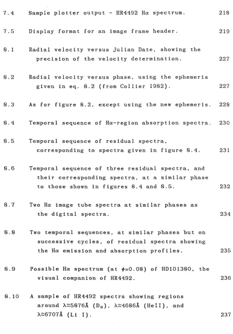
Figure 2.1: Schematic representation of the structure of the Reticon RLxxxxF/30 series photo-diode array.
(based on Livingston et al. 1976)
[image:45.595.74.521.62.339.2]¢,
<:~>2r-~---*---~---.---r---~
START
Ill AS'
VIOEO 2 VIOEO I
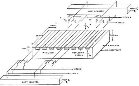
Figure 2.2: Circuit representation of a shift register {based on Joynson et al. 1972).
w
'~>t·I
l
L&.l!i
;i_
C>t-j!rn
<1>2
:.Jo
o->C> time
g
START
Figure 2.3: Time-varying waveforms {clocks, ~1 and ~2 • and the start pulse) for the shift registers.
falling edges. Access to the diode array is accomplished when a charge packet referred to as a 'bit' is loaded into the shift registers first storage node, SN1 , by a rising edge of
clock ~1 being co temporal with a low start pulse. The falling edge of clock ~2 then shifts the start bit into the first address location, AL1 , thereby turning on the first pair of
switches, SWP1 , in the multiplex switch array. That switch
pair is subsequently turned off when the rising edge of ~2
[image:46.595.98.508.66.456.2]alternate pairs of diodes along the array.
2.1.4 The LDA circuit representation
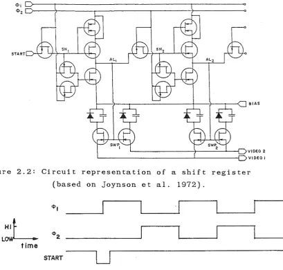
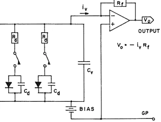
The physical hardware of a video-line in a self-scanning photo-diode array has the equivalent electronic circuit representation shown in figure 2.4. The photo-diodes
<P.
SHIFT REGISTER <P2
START
VIDEO
BIAS
Figure 2.4: Equivalent electronic circuit for a self-scanning photo-diode array.
are represented by an ideal diode in parallel with their diode capacitance, cd. The anode of each diode is connected to the video line through its own shift register addressed multiplex switch, with the 'on' resistance of the switch, Rd' explicitly shown. The cathode of each diode is connected to a common bias line to allow the diodes to be reversed biassed, and to reference the video 1 ine through • on' diodes to the zero signal reference of the external electronics. Each multiplex switch exhibits a small ~0.15 pF capacitance which effectively exists between the video and bias lines. Their parallel sum is represented as a single lumped component by the video capacitance,
C
v Additionally, each switch exhibits a
capacitance between its control line and the video line which is represented by C
[image:47.595.86.514.148.463.2]2.1.5 The Fixed Pattern
When a multiplex switch changes state, the transition in the clock voltage effecting the change will alter the potential across the capacitance C The quantity of charge
cv
required to change the potential of the capacitor must be sourced or sunk by the video line. Thus when a diode is selected by a falling edge during an array scan, and the previous diode is deselected by a rising edge, charge is both
sourced and sunk by the video 1 ine. Imbalance in the C cv capacitances between the two switches due to chip layout and fabrication differences will result in a net charge transfer between the two capacitors and the video 1 ine. The charge transferred is additive to the signal charge on the diode accessed by the video line, and is therefore a component of the fixed pattern of the diode array. Vogt, Tull, and Kelton (1978} have found that the amplitude of the fixed pattern charge is
qfp
=
500,000 e-/h pairs. (2.1) Wood (1979} has claimed that charge pumping in the MOSFET multiplex switches contributes the othercomponent of the fixed pattern. This mechanism removes
major charge from the conducting switch channel connected to the video line when the negative control pulse creates or annihilates the channe 1. This charge is pumped in to the substrate of the switch, reducing the charge on the accessed diode in the additive manner of the fixed pattern.
Both the capacitance
C
of the MOSFET switch gate to cvdrain and gate to source capacitances, and the charge pumping mechanism, are temperature dependent. This requires operation of the diode array at constant temperature to stabilize the
fixed pattern.
2.1.6 Intrinsic LDA Noise Sources
a) Thermodynamic Reset Noise
Charge must flow through a conductor or switch of non-zero resistance to reset the diode capacitance, and so the Johnson-Nyquist voltage noise of the resistance in that reset path (see appendix 2) will cause the reverse bias of the diode voltage to fluctuate during the reset time interval. The corresponding charge fluctuation on the diode capacitance is sampled at the end of the reset period, resulting in an uncertain initial charge on the reset diode. As the resistor noise voltage has an amplitude proportional to ~R. and the noise bandwidth of the resistor-capacitor circuit is inversely proportional to ~R. the reset noise amplitude does not depend on the resistance. Thus to calculate the noise amplitude, the fluctuation energy for a system with one degree of
given by the equipartition theorem, is equated electrostatic energy fluctuation of the capacitor as
.!.
kT
2 [ =
~
cd v2J
freedom, to the
(2.2) The r.m.s. noise in electronic charge units is then found to depend only on the absolute temperature T, and the diode capacitance as
q
=.!.
~
n e r~·~d (2.3)
Additionally, real MOSFET switches can have excess noise of up to ~2 times their Johnson-Nyquist resistor noise, which will increase the thermodynamic noise by up to ~2 (J.A.Hall 1976, p 554).
b) Fixed Pattern Noise
c) Net Intrinsic Detector Noise
Two contributions of reset noise are made to any observation due to resetting the diode at both initialization, and readout. If a reset switch excess noise factor of F is
X
used, and the net charge pumped is called q ,
p the intrinsic detector noise is given by
If F
=
1.2. T=
X
e-/h pairs (Wood,
j2Fx2
a. =1
133 kelvins, 1979), the
kTCd
+ qp e2
cd = 0.6pF, intrinsic
(2.4) and q ~ 8 x 10⁴
p
detector noise is calculated to be approximately 450 electron-hole pairs. However if F = 1 and q = 0 e-/h pairs, then the lower limit
X p
on the intrinsic noise is approximately 290 e-/h pairs.
2.2 Readout Techniques
The diode signal charge must be conditioned by an amplifier attached to the video line to enable subsequent signal processing to determine the integrated photon flux. This amplifier may be characterized as presenting either a high or a low impedance between the video line and the signal ground.
2.2. 1 Video Voltage Level Processing
In figure 2.5 a high input impedance amplifier (see appendix 1) buffers the video line, and a low 'on resistance reset switch interconnects the video and signal ground. As no charge can leak from the video line when buffered by this amplifier, any video line charge variation will appear as a voltage variation on the video capacitance.
a) Reset Switch Action
RESET
BIAS
Figure 2.5: High input impedance amplifier conditioning the video signal.
(d) (b)
Figure 2.6: Equivalent circuits for initialization of {a) diode capacitance, cd. and
(b) video capacitance,
c
.
vlight referred to in section 2.1.2. The diode capacitance charges exponentially to the video bias voltage, vb.
= {Rd+Rr )C d, about 6 ns {Buss
with a et al. time constant of
1976) . The video capacitance is recharged in a similar way, as depicted in figure 2.6b, with a time constant of T
=
R C ,v
r v
about 400 ps. A reset p~riod of N time constants will complete the recharging to one part in exp(N), and can be terminated when the residual charge is negligible compared to the detector noise.At the end of the reset period the video voltage has settled to zero. This would be retained when an ideal reset switch was turned off because no charge would enter or exit the video capacitance. However the control voltage transition that turns off the reset switch will change the voltage across the undesirable capacitance C , requiring the video line to
r
offsets the video line voltage from zero to
where
AV
rp the chargeis the amplitude of the reset control pulse. is t ran sf ered through a capacitance, there
(2.5)
Since is no shot noise associated with it. However the noise waveform on the reset. control line will also feed through to the video line with the dependence of equation 2.5. Thus C must be
r
minimized, and the reset control line noise must be kept to an appropriate value.
b) Readout Operation and Response
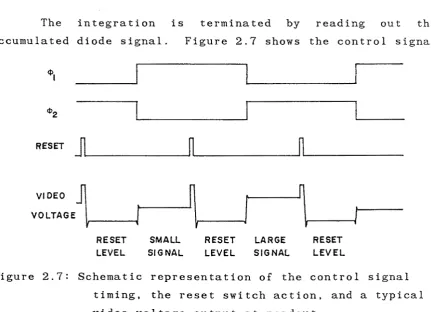
The integration is terminated by reading out the accumulated diode signal. Figure 2.7 shows the control signal
<PI
RESET
jl ____
___.n'---~n~...--
___ _
VIDEO
~
~
f
~
1
I
VOLTAGE
•
,
RESET SMALL RESET LARGE RESET LEVEL SIGNAL LEVEL SIGNAL LEVEL
Figure 2.7: Schematic representation of the control signal timing, the reset switch action, and a typical video voltage output at readout.
timing and a typical video voltage response waveform of the readout. The diode that was accessed by the first falling edge of 4>1 is reset during the middle of its access period; the video voltage is zero during reset, and exhibits the reset feedthrough offset immediately afterwards. Th i s reset vide 0
[image:52.595.81.513.310.622.2]select the next diode. Fixed pattern charge is transferred onto the video line by this process as described in section 2. 1. 5; the video vo 1 tage changes in response to the charge. Also, the selection of the next diode allows the signal of
that diode to be interrogated.
The voltages across the diode and video capacitances, as a function of the charge each holds immediately before the
selection of the diode, are respectively given by qv
' and vr
=
-c-v(2.6) After se lee t ion, the diode charge, video charge, and fixed pattern charge appear on the parallel