Virtual Impedance Impact on Inverter Control Topologies
ISSA, Walid <http://orcid.org/0000-0001-9450-5197> and ELKHATEB, Ahmad
Available from Sheffield Hallam University Research Archive (SHURA) at:
http://shura.shu.ac.uk/23742/
This document is the author deposited version. You are advised to consult the
publisher's version if you wish to cite from it.
Published version
ISSA, Walid and ELKHATEB, Ahmad (2018). Virtual Impedance Impact on Inverter
Control Topologies. In: 7th International Conference on Renewable Energy Research
and Applications (ICRERA). IEEE.
Copyright and re-use policy
See
http://shura.shu.ac.uk/information.html
Sheffield Hallam University Research Archive
Virtual Impedance Impact on Inverter Control Topologies
Walid Issa
1, Ahmad El Khateb
21Sheffield Hallam University, UK, [email protected]
2Queen University, UK
Abstract— The different nature of the energy resources requires high reliable converters and inverters to supply regulated power to the end customer and to ease its integration within a microgrid. In this paper, modeling, design and control of inverters are presented for two different topologies. The study addresses the feasibility of the single loop and double loop control of inverters. The bodeplot technique is used to analyze the system behavior when the inductor and the capacitor currents are used as feedback signals. The different output impedance natures affect the power sharing between inverters and stability. Therefore, a proposed virtual impedance is implemented to enhance the control performance. Simulation results are presented to show the validity of the control strategy.
Index Terms—inverters; droop control; microgrids; output impedance
I
I
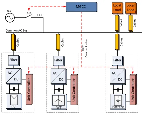
NTRODUCTIONMicrogrid is an aggregated system connecting many distributed generation (DG) units, i.e. renewable energy sources (solar, wind, tidal, etc) or storage systems, to the loads in island mode or to the utility grid in grid-connected mode. It uses inverters to be the link between these units and the loads or the grid. Practically, due to high load demand, the inverters are needed to operate in parallel as shown in Figure. 1. This provides system redundancy and high reliability that is required for flexible microgrid structure. A significant concern of the parallel-operated inverters is robust design of each inverter to have the capability to work in parallel with others without destabilizing the system. Commonly, the droop control is implemented to share the power wirelessly between the inverters. However, the output impedance can affect its accuracy and stability. The literature proposed many control strategies to handle these challenges [1]–[9]. However, the emphasis on the impact of different feedback signals on the voltage control loop and on shaping the output impedance has not been well clarified. The bodeplot technique is used to analyze the system behavior when the inductor and the capacitor currents are used as feedbacks. In addition, different output impedances for parallel inverters degrade the stability. Therefore, a virtual impedance is proposed to stabilize the system and to unify the output impedances nature. Simulation results are presented to show the validity of the control strategy.
The paper is organized as follows; the single and double loop voltage controllers are studied in sections II and III, respectively. Virtual impedance concept for shaping the output impedance is addressed in section V. Section VI discusses the performance of the droop control supported by the virtual impedance along with simulation results.
Grid
STS PCC
MGCC
Sl
o
w
C
o
m
m
u
n
ic
at
io
n
AC DC
U
n
it
C
o
n
tr
o
lle
r
Common AC Bus
Filter
AC DC
U
n
it
C
o
n
tr
o
lle
r
Filter
AC DC
U
n
it
C
o
n
tr
o
lle
r
Local Load
Filter
C
ab
le
s
C
ab
le
s
C
ab
le
s
C
ab
le
s
Local Load
C
ab
le
s
[image:2.612.334.561.266.448.2]PV WT Battery
Figure. 1. General microgrid structure
DC-Link Capacitor
L1
C
L2
PWM Generator
Reference signal
Voltage Controller
Feedback
[image:2.612.344.564.497.617.2]2
II
S
INGLEL
OOPV
OLTAGEC
ONTROLLERAs abovementioned, the link between the energy sources and the load/grid is the inverter. The inverter general structure is shown in Figure. 2. It has IGBT switches which receive the modulated sine wave signals from the voltage controller. This produces high frequency harmonics beside the fundamental sinusoidal signal frequency. The LCL filter is used to mitigate the generated harmonics and to deliver a high quality and low harmonics power signal to the load. Although, L and LC filters topologies are used in the literature, the LCL filter provides higher grid harmonics rejection and supports the design of the output impedance.
In basic voltage source inverters (VSI), a voltage controller loop is used to track the desired input signal and to minimize the error between this signal and the measured output voltage. In this paper, a proportional controller; 𝑘𝑣; supported with
feedforward loop is utilized. The feedforward loop minimizes the steady state error and allows for higher control bandwidth. Figure. 3 shows the model of the LCL filter (physical system) and the voltage control loop. The voltage feedback is measured across the filter capacitor and compared with the reference value. Thereafter, the controller generates the PWM control signals. It can be shown from Figure. 3 that the output voltage is given by
*
( ). ( )
( ) ( ). ( ) o o
o s I s
V s =G s V s −Z (1)
where G(s) is the closed loop transfer function that relates Voto
V* and Z
o is the closed loop output impedance. G(s) is given by,
2 1 1 ( ) 1 v v k G s
L Cs k + =
+ + (2)
[image:3.612.327.582.91.177.2]It is obvious from G(s) that the damping; s term; is zero and this might generate resonance which destabilizes the system and degrades the output signals quality. This can be shown in Figure. 4 by the bodeplot of G(s). The peak appears in the figure indicates the resonance at the frequency of 500Hz. It is easy for any harmonic signal or disturbance to excite this frequency. The large loop gain amplifies this signal and finally distorts the output or destabilizes it. If higher proportional gain is used, it does not damp the resonance but it shifts the resonance frequency to slightly higher values.
III
D
OUBLEL
OOPV
OLTAGEC
ONTROLLERRecently, in the literature, dual loop control has been employed to damp the output filter resonance [10]–[13]. The first loop takes the output voltage as a feedback. The second inner loop takes the inductor L1 or capacitor C current as a feedback as shown in Figure. 5. In both cases the damping can be successfully achieved. However, in this paper, the effect of
selecting any of them on the output impedance shaping is addressed. v k 1 1 L s c I * V o I FeedForward o V + ++ + - + - + -Physical System Digital Controller 2 L s 1 Cs 1 1 L s L I c V
Figure. 3. The model of basic single-loop voltage controller
[image:3.612.333.569.137.493.2]0.1 v k = 0.5 v k = 0.01 v k =
Figure. 4. Bode plot of the single loop voltage controller
v k i k 1 1 L s c I * V o I FeedForward o V + -+ ++ + - + - + -+ -Physical System Digital Controller * I 2 L s 1 Cs 1 1 L s L I c V
Figure. 5. The model of basic double-loop voltage controller
It can be shown from Figure. 5 that G(s) is given by,
2 1 1 ( ) 1 v i v k G s
L Cs k Cs k + =
+ + + (3)
The additional feedback loop is represented by the “s” term in (3) which provides damping. The bode plot in Figure. 6 shows the behavior of the voltage loop with different values of the current feedback gain 𝑘𝑖. More gain provides more damping. It
[image:3.612.341.553.215.385.2]3
21 2 1
( )
1
i
oL
v i
s L s k
Z s L
L Cs k Cs k +
= +
+ + + (4)
If the controller adopts IC, then Zo(s) could be obtained as (5) and will be defined as ZoC(s).
2
1 2 1
( )
1
oC
v i
s L s
Z s L
L Cs k Cs k
= +
[image:4.612.342.559.250.427.2]+ + + (5)
Figure. 7 depicts the bodeplot of the output impedance obtained from (4) and (5). When IL is adopted, the behavior of the output impedance around the fundamental frequency (50Hz) is resistive which means approximately constant gain over wide range of frequency. However, in the IC case the output impedance behaves like an inductor introducing more impedance with the increment of frequency. In both cases, there was a resonance at the natural frequency but it has been damped thanks to the inner current loop.
0.5
i
k =
1
i
k =
5
i
[image:4.612.44.280.295.476.2]k =
Figure. 6. Bode plot of the double-loop voltage controller
IV
D
ROOPC
ONTROLDuring the inverters operation in parallel with each other, droop control techniques might be implemented to achieve good power sharing and to protect any inverter from overloading. Droop control assumes that the output impedance is dominantly inductive or resistive and based on that the droop controller will be different as shown in Figure. 8 and Table 1. 𝜔∗𝑎𝑛𝑑 𝑉∗ are
the nominal frequency and voltage of the inverter output, 𝑚 𝑎𝑛𝑑 𝑛 are the droop gains, 𝑃 𝑎𝑛𝑑 𝑄 are the averaged measured active and reactive powers, respectively.
If parallel inverters are working together to share the power, they should have the same droop equations to achieve the accuracy. This can be satisfied if the output impedances have the same nature of being resistive or inductive. Working under different nature of output impedances without taking the
precaution will degrade the power sharing accuracy and the stability.
V
P
ROPOSED VIRTUAL IMPEDANCEIn this paper, a virtual impedance concept is utilized to unify the nature of the output impedances of inverters working parallel with each other. This impedance mimics the behavior of an inductor or resistor in program. Using programmable impedance rather than a physical one reduces the losses and cost. In addition, being as programmable presents adaptive operation and increases the inverter robustness against network impedance variations. Figure. 9 shows the block diagram of the voltage controller with the virtual impedance Zv(s).
( )
oC s
Z
( )
oL s
Z
Resistive behavior
Fundamental Frequency
Figure. 7. Bode plot of output impedance with IL and IC as feedback
Inverter Voltage
Grid Voltage OR PCC Voltage
o
X
inv
V Vg
Inverter Voltage
o
R Vg Grid Voltage
OR PCC Voltage (a)
(b)
inv
V
[image:4.612.337.551.477.546.2]Figure. 8. Output impedance assumption cases for droop control operation (a) inductive (b) resistive
Table 1 Active and reactive power droop controller
Power control
System Impedance
Pure Inductive
𝒁𝒐= 𝒋𝑿𝒐
Pure Resistive
𝒁𝒐= 𝑹𝒐
Active Power 𝜔 = 𝜔∗− 𝑚𝑃 𝑉
𝑖𝑛𝑣= 𝑉∗− 𝑛𝑃
[image:4.612.324.578.616.688.2]4
vk
i
k
1 1
L s
c I
*
V
o
I
FeedForward
o
V +
-+ ++ +
- +
- +
-+
-Physical System Digital Controller
* I
Virtual Impedance
( )
v Z s
2
L s
1 Cs 1
1 L s
L I
c
[image:5.612.42.294.57.145.2]V
Figure. 9. The model of basic double-loop voltage controller with virtual impedance
With resistive virtual impedance
Without virtual impedance With inductive virtual impedance
Without virtual impedance
(a)
[image:5.612.52.258.193.550.2](b)
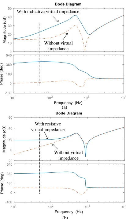
Figure. 10. Bode plot of output impedance with (a) inductive Zv (b) resistive Zv
The new output impedance with virtual impedance can be derived as,
( ) ( ) ( ) ( )
ov o v
Z s =Z s +G s Z s (6)
The nature of Zv could be chosen to be resistive as,
( )
v v
Z s =
R
(7)where 𝑅𝑣 is the resistance of the virtual impedance, or it can be
inductive as,
( )
1
v v
v
s
Z s
s
L
=
+ (8)
where 𝐿𝑣 is the inductance of the virtual impedance and 𝜏𝑣 is
the time constant of the high pass filter used to approximate the derivative in the transfer function of the ideal virtual inductance 𝑍𝑣= 𝑠𝐿𝑣.
Figure. 10 shows the impact of the virtual output impedance on the old output impedances in Figure. 7. In Figure. 10a, an inductive virtual impedance is used to convert the resistive nature to a dominant inductive one. In Figure. 10b, a resistive virtual impedance is used to convert the inductive nature to a dominant resistive one. It is concluded that the virtual impedance has significant impact on the output impedance and with high values it could dominate.
[image:5.612.311.591.420.663.2]In low voltage microgrid network, the network impedance is mainly resistive. Therefore, the droop control for resistive network is selected in this paper. However, the output impedance of each inverter is subject to the implemented feedback and control strategy. It might be a complex impedance rather than pure resistive. Furthermore, the grid-side inductor or any transformers used on the output could change the output impedance to some extent. The virtual impedance concept is used to support the resistivity of the output impedance and its value might be chosen to be 3 times more than the existence reactance as a rule of thumb to consider the dominancy.
Table 2 System Parameter Values
Symbol Description Value
𝐿1 Inverter-side filter inductor 4mH
𝐶 Filter capacitor 25µF
𝐿2 Grid-side filter inductor 2mH
𝑘𝑣 Voltage controller loop gain 0.01
𝑘𝑖 Current controller loop gain 5
𝐿𝑣 Virtual inductance 30mH
𝜏𝑣 Time constant (virtual impedance) 1/1500
𝑅𝑣 Virtual resistance 5 Ω
𝑚 Frequency droop gain 0.05
𝑛 Voltage droop gain 0.05
𝑉𝑜 Voltage set point 115
Vrms
𝑓𝑜 Frequency set point 50 Hz
𝜏 Power measurement filter time constant
0.5 sec 𝐿𝑜1, 𝑅𝑜1 Equivalent output impedance1
(Simulation results)
10mH,1 Ω 𝐿𝑜2, 𝑅𝑜2 Equivalent output impedance 2
(Simulation results)
2mH,6 Ω
Load 1 Load 1 resistance 25Ω
5
Inverter 1I1 I2
Load 1 Load 2
1
o
R
R
o22
o
X
1
o
X
[image:6.612.77.247.58.238.2]Inverter 2
Figure. 11. Simulation network
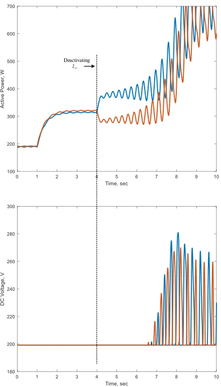
Deactivating ov Z
Figure. 12. Active power and DC voltage responses
VI
S
IMULATIONR
ESULTS [image:6.612.339.561.202.600.2]A microgrid with two inverters systems, as shown in Figure. 11, was built in Matlab/Simulink. The system parameters are in Table 2. Inverter 1 used IL as a feedback while inverter 2 used
IC. Therefore, one would have a resistive output impedance and the other an inductive one. A resistive droop controller was used to share the power between the inverters. The virtual impedance has been implemented for inverter 2 as it has significant inductive impedance. To facilitate the observation of the performance of the virtual impedance, the output power of each
inverter is shown in
[image:6.612.53.273.275.659.2]Deactivating ov Z
6
sharing accuracy. Consequently, the virtual impedance provides more stability room for higher droop gains. Furthermore, the circulating currents between the inverters reflect on the DC side and disturb also the DC link voltages.
VII
C
ONCLUSIONIn this paper, the modeling analysis of the voltage control loops exposed the resonance damping capability of the double-loop strategy compared with the single loop one. In addition, the results highlighted the output impedance behavior when considering different feedback signals. The concept of the virtual impedance has been proposed to unify the output impedance nature of different controlled inverters and to assure proper droop control operation. The simulation results were presented to validate the performance and effectiveness of the proposed controller.
References
[1] W. R. Issa, A. H. E. Khateb, M. A. Abusara, and T. K. Mallick, “Control Strategy for Uninterrupted
Microgrid Mode Transfer During Unintentional Islanding Scenarios,” IEEE Trans. Ind. Electron., vol. 65, no. 6, pp. 4831–4839, 2018.
[2] M. Abusara, J. M. Guerrero, and S. Sharkh, “Line Interactive UPS for Microgrids,” IEEE Trans. Ind. Electron., no. 99, pp. 1–8, 2013.
[3] W. Issa, S. M. Sharkh, R. Albadwawi, M. Abusara, and T. K. Mallick, “DC link voltage control during sudden load changes in AC microgrids,” in IEEE International Symposium on Industrial Electronics, 2017.
[4] W. R. Issa, M. A. Abusara, and S. M. Sharkh, “Impedance interaction between islanded parallel voltage source inverters and the distribution network,” in IET Conference Publications, 2014, vol. 2014, no. 628 CP.
[5] R. Al Badwawi, W. Issa, T. Mallick, and M. Abusara, “DC Microgrid Power Coordination Based on Fuzzy Logic Control,” in 18th European Conference on Power Electronics and Applications, 2016, pp. 1–10.
[6] W. R. Issa, M. A. Abusara, and S. M. Sharkh, “Control of Transient Power during Unintentional Islanding of Microgrids,” IEEE Trans. Power Electron., vol. 30, no. 8, 2015.
[7] W. Issa, S. Sharkh, T. Mallick, and M. Abusara, “Improved reactive power sharing for parallel-operated inverters in islanded microgrids,” Journal of Power Electronics, vol. 16, no. 3. 2016.
[8] W. Issa, M. Abusara, and S. Sharkh, “Control of
Transient Power during Unintentional Islanding of Microgrids,” IEEE Trans. Power Electron., vol. 30, no. 8, pp. 4573–4584, 2014.
[9] W. Issa, A. El Khateb, N. Anani, and M. Abusara, “Smooth mode transfer in AC microgrids during unintentional islanding,” in Energy Procedia, 2017, vol. 134.
[10] R. Ortega, E. Figueres, G. Garcerá, C. L. Trujillo, and D. Velasco, “Control techniques for reduction of the total harmonic distortion in voltage applied to a single-phase inverter with nonlinear loads: Review,” Renew. Sustain. Energy Rev., vol. 16, no. 3, pp. 1754–1761, 2012.
[11] M. A. Abusara, M. Jamil, and S. M. Sharkh, “Repetitive current control of an interleaved grid-connected inverter,” in IEEE International Symposium on Power Electronics for Distributed Generation Systems (PEDG), 2012 3rd, 2012, pp. 558–563.
[12] G. Escobar, P. Mattavelli, A. M. Stankovic, A. A. Valdez, and J. Leyva-Ramos, “An adaptive control for UPS to compensate unbalance and harmonic distortion using a combined capacitor/load current sensing,”
IEEE Trans. Ind. Electron., vol. 54, no. 2, pp. 839– 847, 2007.