WAVES IN CUPRATES
Stephen Edkins
A Thesis Submitted for the Degree of PhD
at the
University of St Andrews
2016
Full metadata for this item is available in
St Andrews Research Repository
at:
http://research-repository.st-andrews.ac.uk/
Please use this identifier to cite or link to this item:
http://hdl.handle.net/10023/9888
Waves in Cuprates
Stephen Edkins
This thesis is submitted in partial fulfilment for the degree of PhD
at the
University of St Andrews
I, Stephen David Edkins, hereby certify that this thesis, which is approximately 40,000 words in
length, has been written by me, and that it is the record of work carried out by me, or principally by
myself in collaboration with others as acknowledged, and that it has not been submitted in any
previous application for a higher degree.
I was admitted as a research student in August, 2012 and as a candidate for the degree of Doctor
of Philosophy in August, 2012; the higher study for which this is a record was carried out in the
University of St Andrews between 2012 and 2016.
Date: 8/9/2016 Signature of candidate
………
.
2. Supervisor’s declaration:
I hereby certify that the candidate has fulfilled the conditions of the Resolution and Regulations
appropriate for the degree of Doctor of Philosophy in the University of St Andrews and that the
candidate is qualified to submit this thesis in application for that degree.
Date: 8/9/2016 Signature of supervisor
………
.
3. Permission for publication:
In submitting this thesis to the University of St Andrews I understand that I am giving permission
for it to be made available for use in accordance with the regulations of the University Library for
the time being in force, subject to any copyright vested in the work not being affected thereby. I
also understand that the title and the abstract will be published, and that a copy of the work may
be made and supplied to any bona fide library or research worker, that my thesis will be
electronically accessible for personal or research use unless exempt by award of an embargo as
requested below, and that the library has the right to migrate my thesis into new electronic forms
as required to ensure continued access to the thesis. I have obtained any third-party copyright
permissions that may be required in order to allow such access and migration, or have requested
the appropriate embargo below.
The following is an agreed request by candidate and supervisor regarding the publication of this
thesis:
PRINTED COPY
No embargo on print copy
ELECTRONIC COPY
No embargo on electronic copy
Date: 8/9/2016 Signature of candidate
………
The study of cuprate high-temperature superconductors has undergone a recent resur-gence due to the discovery of charge order in several families of cuprate materials. While its existence is now well established, little is known about its microscopic origins or its relationship to high-temperature superconductivity and the pseudogap. The aim of the research presented in this thesis is to address these questions.
In this thesis I will report on the use of spectroscopic-imaging scanning tunnelling microscopy (SI-STM) to visualise the short-ranged charge density wave (CDW) in Bi2Sr2CaCu2O8+δ and NaxCa2−xCuO2Cl2. Building on previous measurements of the
intra unit-cell electronic structure of cuprates, I introduce sub-lattice segregated SI-STM to individually address the atomic sub-lattices in the CuO2 plane with spatial
phase sensitivity. Using this technique I establish that the CDW in Bi2Sr2CaCu2O8+δ
and NaxCa2−xCuO2Cl2 has a previously unobserved d-symmetry form factor, where a
breaking of rotational symmetry within the unit cell is modulated periodically in space.
Towards identifying a mechanism of CDW formation, I establish that the amplitude of CDW modulations in the electronic structure are maximal at the pseudogap energy-scale and that these modulations exhibit a spatial phase difference of π between filled and empty states. Together with the doping evolution of the CDW wave-vector this highlights the role of the low-energy electronic structure of the pseudogap regime in CDW formation.
To elucidate the relationship between the CDW and the superconducting condensate I will introduce nanometer resolution scanned Josephson tunnelling microscopy (SJTM). In this approach the Cooper pair (Josephson) tunnelling current between a Bi2Sr2CaCu2O8+δ
sample and a scan-able Bi2Sr2CaCu2O8+δnano-flake STM tip is used to directly visualise
I would first and foremost like to thank my supervisors S´eamus Davis and Andy Macken-zie for their support and guidance, as well as teaching me a great deal. I have benefited greatly from the research environment in both of their groups, of which membership has been a privilege.
The research presented in chapter 4 of this thesis was carried out in close collaboration with Mohammad Hamidian and Kazuhiro Fujita to whom I extend my gratitude for sharing their expertise in spectroscopic-imaging STM. The research presented in chapters 5 and 7 was conducted in collaboration with Mohammad Hamidian and Andrey Kostin. I thank Mohammad for his tutelage in the operation of a cryogenic STM.
The idea of examining the difference between the oxygen sub-lattices of the CuO2 plane
in SI-STM spectroscopic maps to reveal ad-symmetry form factor CDW was originally suggested by Subir Sachdev. I would like to thank him for sharing this with us as well as for useful discussions. I would also like to thank Andrey Chubukov for his very useful comments in the preparation of chapter 6.
Finally, I would like to thank all of my colleagues past and present for their help, advice and friendship, as well as my family for their love and support.
I acknowledge studentship funding from the EPSRC via the Scottish Condensed Matter Center for Doctoral Training under grant number EP/G03673X/1.
Declaration iii
Abstract v
Acknowledgements vii
List of Figures xiii
List of Tables xvii
1 Unconventional Superconductivity and Density Wave Order in Cuprates 1
1.1 Superconductivity . . . 2
1.1.1 What is a Superconductor? . . . 2
1.1.2 BCS Theory of Superconductivity . . . 5
1.2 High-Temperature Unconventional Superconductivity in Cuprates . . . 10
1.2.1 Effective Models of the CuO2 Plane . . . 12
1.2.2 Phase Diagram . . . 13
1.2.3 Anti-Ferromagnetism . . . 14
1.2.4 High-Temperatured-Wave Superconductivity . . . 14
1.2.5 Strange Metal . . . 15
1.2.6 The Pseudogap . . . 16
1.3 Charge Density Waves . . . 17
1.4 Unconventional Density Waves in Cuprates . . . 19
1.5 The Significance of CDW in Cuprates . . . 21
1.6 Organisation of this Thesis . . . 23
2 Spectroscopic-Imaging STM (SI-STM) 25 2.1 Quantum Tunnelling as a Spectroscopy . . . 26
2.1.1 Tunnelling Hamiltonian Formalism . . . 26
2.1.2 Normal - Insulator - Normal (NIN) Tunnelling . . . 27
2.1.3 Superconductor-Insulator-Normal (SIN) Tunnelling . . . 29
2.1.4 Superconductor-Insulator-Superconductor (SIS) Tunnelling . . . . 32
2.2 STM - Principles . . . 32
2.3 STM - Modes of Operation . . . 34
2.3.1 Topography . . . 34
2.3.2 Spectroscopy . . . 36
2.4 SI-STM . . . 37
2.4.1 The Setup Effect . . . 38
2.4.2 Spectroscopic Functionsg(~r, E),I(~r, E),Z(~r, E), andR(~r, E) . . . 40
2.5 Experimental Apparatus . . . 42
2.5.1 STM Head . . . 42
2.5.2 Cryogenics . . . 42
2.5.3 Vibration and RF Isolation . . . 43
2.5.4 Instrumentation . . . 43
2.6 Cuprate Materials . . . 44
2.6.1 Bi2Sr2CaCu2O8+δ . . . 44
2.6.2 NaxCa2−xCuO2Cl2 . . . 46
2.7 Quasi-Particle Interference in Cuprates . . . 47
2.7.1 QPI - A Qualitative Understanding . . . 48
2.7.2 The Octet Model . . . 50
2.8 Mapping Spatial Variations in the Amplitude and Phase of LDOS Mod-ulations . . . 52
3 Sub-Lattice Segregated SI-STM in Cuprates 55 3.1 Data Acquisition Parameters . . . 56
3.2 Atomic Phase Correction Algorithm . . . 57
3.3 Finding Atomic Positions . . . 59
3.4 Sub-Lattice Segregation . . . 60
3.5 Intra-Unit-Cell Spatial Registration of Measurements . . . 62
4 Atomic-scale Electronic Structure of the Cuprate d-symmetry Form Factor Charge Density Wave 65 4.1 Form Factor Decomposition of Modulations in the CuO2 Plane . . . 66
4.2 Proposals for ad-Symmetry Form Factor CDW in Cuprates . . . 70
4.3 SI-STM Signatures of ad-Symmetry Form Factor CDW . . . 72
4.4 Detection of a d-Symmetry Form Factor CDW in Cuprates . . . 75
4.4.1 Form Factor Measurement using Sub-Lattice Segregated SI-STM . 75 4.4.2 Temperature Dependence of the CDW Phenomena . . . 83
4.4.3 Short-Range Unidirectional CDW Domains . . . 84
4.5 Characteristics of CDW Modulations in the Spectral Function . . . 88
4.6 Phase Relationship between the Modulation of Filled and Empty States . 91 4.7 Doping-Dependence of the CDW Wave-vector . . . 94
4.8 Conclusions and Proposed Future Experiments . . . 96
5 The Scanned Josephson Tunnelling Microscope 99 5.1 Fundamentals of SJTM Operation . . . 100
5.2 The Josephson Effect as a Measure of the Superconducting Order Parameter103 5.3 Josephson Current-Voltage Characteristics in Ultra-Small Junctions . . . 109
5.3.1 I(VJ J) Characteristics for Josephson Junctions with Strong Phase Coupling . . . 109
5.3.2 Thermal Phase Fluctuations in Ultra-Small Josephson Junctions . 114 5.3.3 Including both Thermal and Quantum Phase Fluctuations . . . 117
5.3.4 Expected Pair-CurrentIP(V) in Ultra-Small Josephson Junctions 122 5.4 Experimental Strategy for Cuprate SJTM . . . 124
5.5.1 Fabrication of Superconducting Bi2Sr2CaCu2O8+δ Nano-flake Tips 125
5.5.2 Characterisation of Nano-flake Tip Geometry . . . 126
5.5.3 Stability of Tips duringIc(~r) Measurement . . . 129
5.6 Experimental Josephson Current-Voltage Characteristics . . . 130
5.7 Validating SJTM as a Probe of the Order Parameter . . . 135
5.7.1 Imaging the Suppression of Ψ(~r) at Individual Zinc Impurities . . 135
5.7.2 Modulation of Superconductivity by the Bulk Structural Super-Modulation . . . 136
5.8 Conclusions and Future Directions of SJTM . . . 139
5.8.1 Future State of the Art in Condensate Imaging . . . 139
5.8.2 Inelastic Cooper-pair Tunnelling Spectroscopy . . . 141
6 Pair Density Waves in Cuprates 143 6.1 The Pair Density Wave . . . 143
6.2 Experimental Evidence for a Cuprate PDW . . . 149
6.2.1 Decoupling of Superconductivity between the CuO2 Planes . . . . 149
6.2.2 Photoemission Spectra . . . 153
6.3 Coupled Order Parameters . . . 154
6.4 Coupling of PDW to Other Order Parameters . . . 156
6.4.1 Coupling to CDW . . . 156
6.4.2 Coupling to SDW . . . 157
6.4.3 Coupling to Uniform Superconductivity . . . 157
6.5 Theoretical Proposals for a Cuprate PDW . . . 158
6.5.1 Variational Numerical Calculations . . . 159
6.5.2 PDW within Mean-Field Models . . . 160
6.5.3 Amperean Pairing . . . 160
6.5.4 Spin-Fermion “Hot-Spot” Models . . . 163
6.6 Experimentally Distinguishing PDW Scenaria . . . 164
7 Detection of a Cooper-pair Density Wave in Bi2Sr2CaCu2O8+δ 167 7.1 Four Unit-Cell Periodic Modulations in the Cooper-Pair Current . . . 168
7.2 Discussion of Ic(~r) Modulations as a Pair Density Wave . . . 171
7.3 Conclusions . . . 173
8 Summary and Future Directions 175 A Publications Arising from Doctoral Studies 179 A.1 Piezoelectric Strain Tuning . . . 179
A.2 Spectroscopic Imaging STM of the Cuprate CDW . . . 179
A.3 Scanned Josephson Tunnelling Microscopy . . . 180
B A Form Factor Description of Local Rotational Symmetry in Density
Waves 181
C Calculating Sub-lattice Fourier Transforms 185
E Topographic Imaging of the Cuprated-Symmetry Form Factor Charge
Density Wave 193
F Absence of Setup Effect in Relative Spatial Phase Measurements 197
G Antiphase Modulation of Filled and Empty States at |E|= ∆1 201
H Measuring RN for Cuprate SJTM 203
1.1 Phase Stiffness in a 1D Crystal . . . 2
1.2 Bogoliubov Quasi-Particles . . . 9
1.3 The CuO2 Plane . . . 10
1.4 A Charge Transfer Insulator . . . 11
1.5 Cuprate Phase Diagram . . . 14
1.6 d-Wave Superconducting Gap and Pseudogap . . . 15
1.7 Bare Particle-Hole Susceptibility in d=1,2 & 3. . . 18
1.8 CDW Enhancement upon Suppressing Superconductivity . . . 22
2.1 Schematic of Vacuum Tunnelling . . . 29
2.2 Schematic of STM Operation . . . 33
2.3 Atomically Resolved Topograph . . . 35
2.4 STM Tunnelling Conductance Spectrum . . . 36
2.5 IIllustration of SI-STM . . . 38
2.6 The Setup Effect . . . 40
2.7 STM Head . . . 43
2.8 Passive Vibration Isolation . . . 44
2.9 SI-STM Instrumentation . . . 45
2.10 Unit Cell of Bi2Sr2CaCu2O8+δ . . . 47
2.11 Unit Cell of NaxCa2−xCuO2Cl2 . . . 48
2.12 The Octet Model . . . 50
2.13 d-Wave Superconducting Gap and Fermi Surface in Bi2Sr2CaCu2O8+δ . . 53
3.1 Sub-lattice Segregation for NaxCa2−xCuO2Cl2 . . . 61
3.2 Spatially Registered B=8.5T and B=0T Topographs . . . 63
4.1 The Three Sub-lattices in the CuO2 Plane . . . 66
4.2 Intra-Unit-Cell Electronic Structure Symmetry in the CuO2 Plane . . . . 68
4.3 Types of CuO2 Intra-Unit-Cell Density Waves . . . 71
4.4 Experimental Signatures of d-Symmetry Form Factor CDW . . . 74
4.5 Oxygen site-specific imaging and segregation of R(~r) . . . 77
4.6 Sub-lattice Segregation for Bi2Sr2CaCu2O8+δ . . . 78
4.7 Sub-lattice Phase-Resolved Fourier analysis revealing ad-Symmetry Form Factor . . . 79
4.8 Predominance of the d-Symmetry Form Factor . . . 81
4.9 Representative Unidirectional Domains CDW . . . 82
4.10 Unidirectionald-Symmetry Form Factor CDW Domains in the Supercon-ducting and pseudogap phases . . . 85
4.11 Underdoped Cuprate Tunnelling Spectrum . . . 88
4.12 Dispersion of Bogoliubov Quasi-particle and CDW Modulations . . . 89
4.13 PSD for Measuring Form Factor Amplitudes . . . 90
4.14 Equivalent representation ofd-symmetry Form Factor modulations . . . 91
4.15 Energy Dependence of Form Factor Amplitudes . . . 92
4.16 Relationship between CDW Modulations of filled and empty states . . . . 93
4.17 Doping Dependence of Fermi Surface and CDW Wave-Vector . . . 95
5.1 Conceptual Operation of SJTM . . . 101
5.2 The RCSJ Model . . . 110
5.3 The Tilted Washboard Potential . . . 111
5.4 I(VJ J) for Coherent Phase Dynamics . . . 112
5.5 Lumped Element Representation of Shunting by Electromagnetic Envi-ronment . . . 114
5.6 The Effect of a Parasitic Capacitance . . . 116
5.7 I(VJ J) with Strong Thermal Fluctuations . . . 117
5.8 Inelastic Cooper-pair Tunnelling. . . 120
5.9 I(VJ J) with Strong Quantum and Thermal Phase Fluctuations . . . 123
5.10 Single-Particle Tunnelling Spectrum with Superconducting Tip . . . 125
5.11 Schematic of SIS Single-Particle Tunnelling Between d-Wave Supercon-ductors . . . 127
5.12 Spectroscopic/topographic data from two distinct Bi2Sr2CaCu2O8+δ tips . 128 5.13 Simulation of topography with BSCCO nanoflake tip . . . 129
5.14 Demonstration of Tip Stability during SJTM Operation . . . 130
5.15 SJTM circuit model . . . 132
5.16 Experimental SJTMI(VJ J) Characteristics . . . 134
5.17 TypicalIc(~r) Measurement . . . 135
5.18 The Suppression ofIc at Individual Zinc Impurities . . . 137
5.19 Sequence of measured Ic(r) along line through a Zinc Impurity . . . 138
5.20 Spatial Variations and Modulations in Cuprate Energy Gaps . . . 139
5.21 Ic(~r) Modulation due to Crystal Super-modulation . . . 140
6.1 Cooper Pairing at Non-Zero Centre of Mass Momentum . . . 145
6.2 Formation of the FFLO State from Zeeman Split Fermi Surfaces . . . 147
6.3 Spin Stripe Order at x=1/8 in La2−xBaxCuO4 . . . 152
6.4 PDW like Features of the Anti-Nodal Gap in Bi2Sr2CuO6+δ . . . 154
6.5 Striped Variational Solutions to the t-J Model . . . 159
6.6 Amperean Pairing . . . 162
6.7 Cartoon of Orthogonal CDW/PDW State in a Spin-Fermion Model . . . 163
7.1 Nanometer Resolution Imaging of the Superconducting Condensate by SJTM . . . 169
7.2 Visualising the Cooper Pair Density Wave in Bi2Sr2CaCu2O8+x . . . 170
C.1 Sub-lattice decomposition ofd-Symmetry Form Factor CDW . . . 187
C.2 Fourier Analysis of CDW using the Convolution Theorem . . . 189
D.2 Sub-Lattice Segregated Fourier Analysis of CDW in NaxCa2−xCuO2Cl2 . 192
E.1 d-Symmetry Form Factor CDW Visualised through Topography . . . 195
F.1 Establishing the Absence of a Setup Effect using Simultaneous Topogra-phy . . . 199
G.1 Energy Dependent Phase Difference . . . 202
6.1 PDW Phases in a Quasi Two-Dimensional Tetragonal Lattice . . . 149 6.2 PDW Scenaria in Cuprates . . . 165
fostered my interest in science and technology.
Unconventional
Superconductivity and Density
Wave Order in Cuprates
Superconductors, known for their ability to conduct electricity without resistance, are fairly common in nature. This is a result of the fact that, despite the strong interac-tions between their electrons, most of the metals we know can be described by a liquid of electron-like quasi-particles. This liquid, known as a Fermi liquid, is intrinsically unstable to the formation of superconductivity. The vast majority of these supercon-ductors only superconduct below a transition temperature which is within a few degrees of absolute zero, limiting their widespread commercial exploitation.
This thesis concerns a family of superconductors whose superconducting transition tem-peratures were unprecedentedly high upon their discovery by Bednorz and Muller in 1986 [1]. These materials, known as cuprates because their common constituents are copper and oxygen, won Bednorz and Muller the 1987 Nobel Prize for Physics for their discovery [2]. Although the cuprates lost their status as the highest temperature super-conductors in the past couple of years to hydrides at ultra-high pressures, they retain the name “high temperature superconductors” and are still a system of unparalleled interest [3]. The high transition temperatures of the hydrides seems to be well under-stood in terms of extensions of traditional theory, but the mechanism of the more exotic superconductivity in cuprates is still the subject of active debate.
In addition to superconductivity, the cuprates also exhibit what is called a charge density wave (CDW). In a CDW the charge density in the material modulates with a periodicity that is different from that of the material’s crystal structure. In this thesis I utilise recent developments in scanning tunnelling microscopy (STM), and develop nanometer-resolution scanned Josephson tunnelling microscopy (SJTM) with the aim of elucidating the role of CDW in the physics of these materials.
1.1
Superconductivity
1.1.1 What is a Superconductor?
The concept of spontaneous symmetry breaking is a cornerstone of 20th century physics [4]. In condensed matter physics we have chosen to classify different phases of matter by the symmetries they break. If the state of a system is not invariant under an element of the symmetry group of the Hamiltonian to which it is a statistical solution, then it is said to break the corresponding symmetry.
As an example take a macroscopic number of particles in free space which interact with each other. The Hamiltonian which governs these particles is invariant under spatial translations. However, the particles could condense into a crystal. This is clearly a state which breaks translational symmetry as depicted in figure 1.1 in one dimension.
Figure 1.1: Cartoon one-dimensional crystal with lattice constanta0. The distance
between thejth andj+ 1th particle is stretched by a distance ∆x.
The crystal has broken translational symmetry by “choosing” where to fix thejth par-ticle in space, the positions of the others following directly from the lattice constanta0
We can expand the density of particles in Fourier components,
hn(x)i=n0+Re{nQ(x)eiQx}+..., (1.1)
whereQ= 2π/a0. The complex field nQ(x) =|nQ(x)|eiarg{nQ(x)} is a sensible choice of
order parameter for our crystalline phase. It will be zero above the melting temperature of the crystal and non-zero below. In this language, choosing a particular position for thejth particle corresponds to choosing a particular phase ofnQ(x),φ(x) = arg{nQ(x)}.
This corresponds to spontaneously breaking a U(1) symmetry. The concept of spatial phase in a crystal will be a key theme in this thesis which I will return to in chapters 3 and 4, where the spatial phase sensitivity of spectroscopic-imaging STM (SI-STM) will be used to probe the intra unit cell electronic structure of cuprates.
Part of the utility of the classifying phases of matter by their broken symmetries is that the broken symmetry has an attendant generalised rigidity [4], i.e a stiffness to spatial gradients in the order parameter. For the crystal there is a very tangible rigidity to changing the separation between any two atoms, akin to stretching a spring. If we consider the order parameter description of this crystal then we can recast this as a phase rigidity. To change the distance between two particles,j and j+ 1 by an amount ∆xrequires a phase gradientφ(xj+1)−φ(xj) =Q∆x, for which there is an energy cost.
If we make the constraint that the order parameter amplitude is spatially uniform so thatnQ(x) =|n0|eiφ(x) we can make the following expansion of the free energy
F[φ(x)] =F0+
Z
dxK(∇φ(x))2+.... (1.2) where K is a positive constant and F0 is the energy of the uniform crystal. Here there
is a clear energy cost to gradients in φ(x); a phase rigidity. Viewed this way, that fact that crystals behave like rigid bodies is a natural consequence of their phase stiffness, which in turn is a direct consequence of breaking translational symmetry.
An order parameter describing this phase would be a complex scalar field of the form Ψ(~r) =|Ψ(~r)|eiφ(~r). If this order parameter is non-zero then everywhere this state breaks the U(1) phase symmetry of the Hamiltonian. We can construct a Ginzburg-Landau expansion of the Helmholtz free energy functional in this order parameter
F[Ψ(~r)] = Z
d3~rα(T−Tc)|Ψ(~r)|2+
β
2|Ψ(~r)|
4+ 1
2m|
−i~∇ −2e ~A
Ψ(~r)|2+|B~|
2
2µ0
+...
(1.3) where A~ is the magnetic vector potential and B~ = ∇ ×A~ [5]. This is the simplest expansion of an electrically charged complex scalar field that is gauge invariant. In anticipation of the microscopic description of a superconductor in terms of Cooper-pairs of electrons I have given the field a charge 2ewhere eis the electron charge. That the field is scalar implies that these Cooper-pairs are in a spin-singlet state. Below a critical temperatureTcthe order parameter Ψ will become non-zero to minimise this free energy.
Now consider the case where the order parameter amplitude is everywhere constant so that Ψ(~r) =|Ψ0|eiθ(~r). We can write the free energy functional as,
F[θ(~r)] =F0+ρs
Z
d3~r
∇θ(~r) +2e
~
~ A
2
+..., (1.4)
with F0 the free energy of the uniform superconducting state and ρs, the superfluid
stiffness, given by
ρs= ~
2
2m|Ψ0|
2 . (1.5)
It is informative at this point to revisit the discussion of crystallisation and the analogies that can be drawn between that process and the formation of the superconducting condensate. The 1D crystal considered above breaks a global U(1) symmetry by choosing a lattice phase. This broken symmetry results in a generalised rigidity, a rigidity against deforming the inter-particle separation from its equilibrium value. This can be expressed as a phase stiffness. This phase stiffness essentially defines this 1D crystalline state of matter.
The same is true of the superconductor. It breaks a U(1) phase symmetry resulting in a stiffness, ρs, to gradients in the phase of the order parameterθ(~r). Below I will show
phase symmetry and its resultant phase stiffness. This phase stiffness is the defining property of a superconductor.
Making a Legendre transformation, g =f −µ0H~ ·B~, of equation 1.4 to the Gibbs free
energy and minimising with respect to variationsδ ~A yields a current
~js=−2e
~ρs
∇θ(~r) +2e
~
~ A
. (1.6)
This expression has profound consequences.
The first is that superconductors should expel magnetic flux from their bulk: the Meiss-ner effect [6]. To see this we can take the curl of both sides resulting in the following differential equation for the magnetic field
∇2B~ = B~
λ2 , (1.7)
where λ= p~2/4µ0e2ρs is a phenomenological constant called the penetration depth.
This implies that magnetic fields must exponentially decay into the bulk of a supercon-ductor over a length scale λ. Thus superconductors expel magnetic fields from their bulk.
To act as perfect diamagnets and expel magnetic fields from their bulk, superconductors must produce screening currents that oppose an applied magnetic field. These must be equilibrium currents, implying that they experience zero resistance. These zero resis-tance equilibrium currents suggest the possibility of non-equilibrium currents with zero resistance which are a hallmark of superconductivity and give it its name.
A zero resistance transport current, the passing of current without any voltage dropped, was measured by Kamerlingh Onnes in mercury in 1911, heralding the discovery of superconductivity [7]. Clearly this property is remarkable and of great technological importance. However, it is not fundamental to superconductivity in the way that the equilibrium screening currents of the Meissner effect are.
1.1.2 BCS Theory of Superconductivity
with a paper from Bardeen, Cooper and Schrieffer, the exposition of what is now called the BCS theory of superconductivity [8].
Prior to this Cooper had shown that, in the presence of a Fermi surface and arbitrarily weak attractive interactions, two quasi-particles with opposite momenta are unstable to the formation of a bound state or Cooper pair. One way of demonstrating this instability of the Fermi liquid is to calculate the particle-particle (pairing) susceptibility within the random phase approximation (RPA),
χpp(~q, ω) =
χ0pp(~q, ω) 1 +gχ0
pp(~q, ω)
, (1.8)
which measures the response to a field that acts to pair particles [9]. Here g is an effective point-like interaction between Fermi liquid quasi-particles with spin σ of momentum~k
and energyσ,~k. χ0pp is the bare (non-interacting) susceptibility,
χ0pp(~q = 0, ω) = 1 Ω
X
~k
f(σ,~k)−f(−σ−~k) ~ω−σ,~k−−σ,−~k+i0+
, (1.9)
where f(σ,~k) is the occupation factor of a quasi-particle state labelled by~k and σ and Ω is the volume of the system.
In the limit whereω, ~q →0
χ0pp(~q= 0, ω= 0)∼N(= 0) log(Λ/T) . (1.10) Here N( = 0) is the density of states of the Fermi energy and Λ is an ultra-violet cut-off [9]. Equation 1.10 shows that χ0pp(~q = 0, ω = 0) is positive and logarithmically divergent with decreasing temperature. This results from the fact that, in the presence of time reversal symmetry,σ,~k =−σ,−~k. Examination of equation 1.8 then shows that
for any arbitrarily small attractive interaction (g <0) the particle-particle susceptibility will diverge at non-zero temperature. This signals an intrinsic instability of the metal towards forming Cooper pairs.
expand the orbital wave-function in spherical harmonics (which is valid in free space), spin-singlet pairs will have angular momentum quantum number l = 0,2, .. which we call s- and d-wave respectively, by analogy with the orbitals of the hydrogen atom. Likewise, spin-triplet superconductors will have l = 1,3, ... corresponding to p- and f-wave respectively.
With the insight that the Fermi liquid is unstable to the formation of Cooper-pairs in the presence of an attractive interaction, Bardeen, Cooper and Schrieffer considered the equivalent of the Hamiltonian,
ˆ
H =X
~kσ
~kˆc~†kσcˆ~kσ+
X
~k~q
V~k~qcˆ~†k↑ˆc†−~k↓ˆc−~q↓ˆc−~q↑, (1.11)
where
V~k~q=
−V if|~k|and |~q| ≤~ωc
0 otherwise
(1.12)
so that there is an attractive interaction between quasi-particles up to a energy cut-off
~ωc away from the Fermi energy. It is manifest in the form of the interaction chosen
that any Cooper pairs formed will be of the spin-singlet type and thus must have an even parity orbital wave-function.
Anticipating the formation of a condensate of Cooper-pairs BCS introduced the varia-tional wave-function,
|ΨBCSi=
Y
~k
|u~k|+|v~k|eiθˆc
†
~k↑cˆ † −~k↓
|0i , (1.13)
where|u~k|2+|v~k|2 = 1,θis an arbitrary phase factor and|0i corresponds a sea of Fermi
liquid quasi-particle states filled up to the Fermi wave-vector ~kF [8]. This many-body
wave-function takes the form of a superposition of a filled Fermi surface plus a Fermi surface with 0,1,2,... Cooper pairs. Making a connection with the previous section, this is a coherent state of Cooper pairs, with minimum uncertainty in the phase and indefinite particle number. It thus manifestly breaks phase symmetry and we can associateθwith the phase of the condensate.
BCS went on to find the parameters u~k and v~k of the ground state by the variational
between a superconductor and either a normal metal or another superconductor. For this we will need to know the single-particle excitation spectrum of the superconductor. To calculate this one can follow Bogoliubov [10] who considered the following mean-field decoupling of equation 1.11
ˆ
H =X
~ kσ
~kˆc~†kσˆc~kσ+
X
~kσ
∆~kcˆ†~k↑cˆ†−~k↓+ ∆~∗kˆc−~k↓ˆc−~k↑ , (1.14)
with mean-field ∆~k given by the self-consistency condition
∆~k=
X
~ q
V~k~qhˆc−q~↓cˆ~q↑i. (1.15)
The Hamiltonian in equation 1.14 can be diagonalised by a canonical transformation. First we introduce new quasi-particle operators which are mixtures of electron and hole creation operators,
α~k=u~kˆc~k,↑−v~kcˆ†−~k,↓ (1.16)
β~k=u~kcˆ−~k,↓+v~kˆc~†k,↑ , (1.17)
where|u~k|2+|v~k|2 = 1 to retain Fermionic anti-commutation relations. In terms of these
operators the Hamiltonian can be written in the diagonal form,
ˆ
H=X
k
Ek
α~†
kα~k+β
†
~kβ~k
, (1.18)
whereE~k=
q
2
~k+|∆~k|2and the coefficientsu~kandv~kthat diagonalise the Hamiltonian
are
|v~k|2= 1− |u~k|2 =
1 2
1− ~k
E~k
. (1.19)
Equation 1.18 shows that there is a gap ∆k to excitations of the superconductor as
shown in figure 1.2. On exceeding the gap energy, the excitations are described by acting on the BCS ground state with a mixture of particle and hole creation operators. For example α~†
k creates a quasi-particle which for E~k = ∆~k is an equal admixture of
electron and hole creation operators, but with increasing E~k the admixture of hole
creation operator gradually diminishes. These quasi-particles, created byα~†
kand β
†
~ k are
Figure 1.2: (a)Excitation spectrum for BCS superconducting state with~k =vF(~k−
~kF) ands-wave superconducting gap ∆k= ∆. Dashed lines are the bare band|~
k|. (b)
|u~k|2 and|v~k|2 for the excitation spectrum shown in (a). At E~k =|∆| the Bogoliubov
quasi-particle creation operators are an equal admixture of hole and electron creation operators but with increasing energy rapidly becomes the excitations of the bare band.
What form does this gapping of the Fermi surface take? As I will discuss below, the conventional superconductors have ans-wave gap that has the same sign on all parts of the Fermi surface, leading to a fully gapped Fermi surface. Cuprate superconductors on the other hand have a gap that changes sign upon rotation by 90◦, and thus necessarily has points where the gap goes through zero called nodes [11]. At these points there are gapless Bogoliubov quasi-particle excitations.
In the conventional superconductors considered by BCS, the effective attractive inter-action is a result of the electron-phonon interinter-action. An electron moving through the lattice disturbs it, leaving a region of net positive charge in its wake. Another elec-tron passing through will feel an attraction to this cloud of positive charge through the Coulomb interaction. Thus, there is an effective attractive interaction between the two electrons at the same point but at different times.
Having discussed the nature of and mechanism behind conventional superconducting states I will now go to discuss the cuprate high temperature superconductors whose superconductivity in unconventional in both its nature and mechanism.
1.2
High-Temperature Unconventional Superconductivity
in Cuprates
The common constituent of all cuprate superconductors are the copper oxide planes shown in figure 1.3 (a). These copper oxide layers are incorporated between inert ionic layers which can act as a source of holes or electrons for the CuO2 layers, thereby doping
them.
Figure 1.3: (a) CuO2 plaquettes consisting of copper 3dx2−y2 and oxygen 2px,y
Each CuO2 plaquette contains one copper atom and two oxygen atoms. Much focus in
this thesis will be given to a breaking of rotational symmetry within the unit cell via an inequivalence of these two oxygen sites, which I will term x and y-directed oxygens respectively.
Each copper contributes a singly occupied 3dx2−y2 orbital. x and y directed oxygens each contribute a doubly occupied 2px or 2py orbital respectively. The compact nature
of the 3dx2−y2 orbital leads to a large energetic cost for double occupation arising from the Coulomb interaction. In cuprates the difference in energy between a singly and doubly occupied 3dx2−y2 orbital, Ud, is ∼7-10 eV [13].
This onsite Coulomb repulsion, or Hubbard Ud, splits the spectral weight from the
3dx2−y2 orbitals into upper and lower Hubbard bands with a gap, Ud, for charge exci-tations between them as shown in figure 1.4. If this were the full story then this would lead to an insulator of the Mott-Hubbard type where hopping of electrons is prohibited by the energetic cost of moving an electron from one Cu sites to doubly occupy another. Cuprates however fall into a related class of insulators, proposed by Zaanen, Sawatsky and Allen, known as charge-transfer insulators [14].
Figure 1.4: (a)Schematic depiction of single-particle spectrum for a Mott-Hubbard
insulator showing smallest optical gap, Ud, is between the lower and upper Hubbard
bands (UHB and LHB) derived from the Cu 3dx2−y2 orbitals. (b)Depiction of a charge
In a charge-transfer insulator the smallest gap for charge excitations is to take an electron from an oxygen 2p orbital and put it on the copper site. In cuprates, x-ray absorption spectroscopy has shown that this is the smallest charge excitation gap with value, ∆∼
2−4eV, which is smaller than Ud [15–17]. The consequence of this is that when holes
are first doped into the CuO2 plane, it is into the oxygen 2p orbitals.
1.2.1 Effective Models of the CuO2 Plane
An effective model describing the essential physics of the CuO2 plane is the three-band
Hubbard model with Hamiltonian [18],
ˆ
H=−tdp
X
hi,jiσ
ˆ
d†iσpˆjσ+h.c
−tp
X
hj,j0iσ
ˆ
p†jσpˆj0σ+h.c
+t0p X
hj,j00iσ
ˆ
p†jσpˆj00σ+h.c
+ ∆X
jσ
ˆ
np,jσ+Ud
X
i
ˆ
nd,i↑ˆnd,i↓+Up
X
i
ˆ
np,j↑nˆp,j↓+V X
hi,ji ˆ
nd,inˆp,j , (1.20)
where ˆdiσ annihilates a hole with spinσ on the Cu 3dx2−y2 orbital at site i, and ˆpjσ is that on the O 2p orbital at site j. The number operators are given by ˆnd,iσ = ˆd†iσdˆiσ
and ˆnp,jσ = ˆp†jσpˆjσ. The summation hi, ji represents that over nearest-neighbour Cu-O
bonds while the sum over hj, j0i and hj, j00i are for nearest and next-nearest-neighbour O-O bonds as shown in figure 1.3 (b). Up is an onsite Coulomb repulsion for the oxygen
2p orbitals and V is an inter-site repulsion between electrons on nearest-neighbour Cu and O sites.
Typically however, the theoretical starting point for understanding of cuprate physics is that of the single band Hubbard ort−J model. Zhang and Rice justified the potential applicability of these single-band models through the insight that a hole doped onto into the CuO2 plane might delocalise over the 4 oxygens surrounding it and form a
Hamiltonian,
ˆ
H =−t X
hi,jiσ
PG
ˆ
c†iσˆcjσ+h.c
PG+J
X
hi,j
ˆ
~ Si·S~ˆi−
1 2ˆninˆj
, (1.21)
whereci,σ annhiliates a hole on siteiwith spin σ,S~ˆi is the spin operator andPG is the
Gutzwiller projection operator that projects out doubly occupancy of any site.
It is well known that this t−J Hamiltonian can be obtained from the single band Hubbard Hamiltonian,
ˆ
H=−t X
hi,jiσ
ˆ
c†iσcˆjσ+h.c
+UX
i
ˆ
ni↑nˆi↓ , (1.22)
by pertubatively intergrating out high energy degrees of freedom in the the limitU/t >>
1 [20], shrinking the relevant Hilbert space and leading to a more practically soluble model. Thus, the physics of the CuO2 plane is often approached from one of these
single-band models. However, as we will see in chapter 4 this potentially misses some key aspects of cuprate phenomenology.
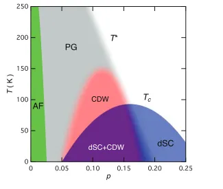
1.2.2 Phase Diagram
A schematic phase diagram of hole-doped cuprates is shown in figure 1.5. The most well-defined features of the phase diagram are an insulator that becomes anti-ferromagnetic for T < TN at small hole concentration, p, and a dome of high temperature
250
200
150
100
50
0
T
)
K (
0.25 0.20
0.15 0.10
0.05 0
p
dSC
PG
CDW
AF
T*
T
c [image:35.596.128.453.90.365.2]dSC+CDW
Figure 1.5: Schematic hole-concentration - temperature phase diagram of cuprate
superconductors. The green region labelled AF represents an anti-ferromagnetic in-sulating state. The blue region labelled dSC is a dome of high temperature d-wave superconductivity with critical temperatureTc. The grey shaded region denotes that
pseudogap regime, with characteristic temperature T∗, terminating at hole-doping,p∼
0.19 holes per Cu. The pink area is a dome of charge density wave order.
1.2.3 Anti-Ferromagnetism
The anti-ferromagnetism of the undoped cuprates arises from the Anderson super-exchange mechanism, where virtual hopping of electrons between Cu 3dx2−y2 through the O 2p orbitals lowers the energy if the spins of the electrons localised in 3dx2−y2 orbitals are anti-aligned [20]. This leads to N´eel type anti-ferromagnetic order with a critical temperature TN. Doping of holes into the O 2p orbitals frustrates this
anti-ferromagnetic coupling and leads to a rapid suppression of TN with hole doping.
1.2.4 High-Temperature d-Wave Superconductivity
learn how such high transition temperatures arise and how we might extend this towards room temperature is the aspiration behind research into cuprate superconductors.
Cuprate superconductivity is also unconventional in a more well defined sense: its pairing symmetry. In the conventional superconductors discussed in section 1.1.2 the pairing amplitude transforms like the trivial representation of the point group (s-wave). In cuprates it is well established that the pairing amplitude isdx2−y2 like [11]. It changes sign under 90◦ rotations, leading to four line nodes in the gap function along the (1,1) directions. In a tetragonal lattice, the pairing amplitude would transform like the B1g
[image:36.596.221.414.279.499.2]representation of the point group, breaking lattice rotation symmetry.
Figure 1.6: The form of the superconducting gap (∆SC) and pseudogap in momentum
space. Thedx2−y2like superconducting gap (blue) has nodes along the (kx, ky) = (1,1)
directions whereas in the pseudogap regime (Tc< T < T8) there are arcs of zero-energy
excitations (shown in red). Reproduced from reference [22] with permission.
1.2.5 Strange Metal
This, and similar behaviour seen in other materials [23], thus far defies a coherent theoretical understanding and represents one of the greatest outstanding challenges in our understanding of the cuprates.
1.2.6 The Pseudogap
The hole doped cuprate phase diagram harbours a region which exhibits a pseudogap, i.e a partial suppression of spectral weight at the Fermi energy forTc < T < T∗. This
region is indicated by the grey shaded region labelled PG in figure 1.5. The existence of such a suppression has been indicated by a large number of experimental techniques [22].
Angular Resolved Photoemission Spectroscopy (ARPES) has given particular insight into how the pseudogap forms in momentum space [24, 25]. For Tc< T < T∗ there are
coherent quasi-particle peaks in a narrow region of momenta near the zone-diagonals (nodal regions). In contrast, the anti-nodal region of the Brillouin zone exhibits a suppression of low energy spectral weight over the pseudogap energy scale and an absence of any quasi-particle peaks. This is illustrated in figure 1.6. With increasing doping the coherent region grows and eventually forms a full Fermi surface of coherent quasi-particles.
STM of underdoped cuprates also exhibits a pseudogap in tunnelling spectroscopy mea-surements [26–28]. This is characterised by a suppression of tunnelling conductance near the chemical potential over a range of bias voltages ∆0/e, the magnitude and doping
dependence of ∆0 being consistent with other measures of the pseudogap energy scale.
A lack of coherence in the anti-nodal regions of the Brillouin zone is also detected by STM quasi-particle interference measurements, albeit for T < Tc. In these
measure-ments, modulations in the tunnelling conductance caused by scattering interference of Bogoliubov quasi-particles are not observed for states beyond the anti-ferromagnetic zone boundary in momentum space forp <0.19. Forp >0.19, interference patters aris-ing from Bogoliubov quasi-particles extendaris-ing out to the full Brillouin zone boundary are observed [29, 30]. The precise relationship between this and the Fermi arcs observed by ARPES is not clear, because forT < TcARPES indicates coherent quasi-particles in
Measurements indicating the existence of a plethora of broken symmetries in the pseu-dogap regime have been reported, including time-reversal, lattice-translational, point-group, spin-rotation and time-reversal symmetry-breaking [32–37]. Of central interest in this thesis are those that break lattice translational symmetry. I will now go on to discuss translational symmetry breaking as well as its discovery and phenomenology in cuprates.
1.3
Charge Density Waves
A charge density wave is a state of matter that breaks lattice translational symmetry whilst preserving time-reversal, spin rotation and phase symmetries. In such a state any density-like observable, i.e one that is invariant under time-reversal, spin-rotation and phase-rotation operations, will be modulated with a periodicity different to that of the lattice. One such quantity is charge density, which gives its name to this state of matter [38].
For the square lattice of the CuO2plane we can expand the charge density wave in order
parameters as follows:
hψˆσ†(~r1) ˆψσ(~r2)i=
F(~r1−~r2)
h
ρQ~x(R~)ei ~Qx· ~ R+ρ
−Q~x( ~
R)e−i ~Qx·R~ +ρ
~ Qy(
~
R)ei ~Qy·R~ +ρ
−Q~y( ~
R)e−i ~Qy·R~i+...,
(1.23)
where R~ = (~r1 +r~2)/2 and ρQ~x, ρ−Q~x, ρQ~y and ρ−Q~y are charge density wave (CDW)
order parameters. They are complex scalar fields that carry momenta Q~±x and Q~±y
running along orthogonal directions ~x and ~y. A constraint ρQ~x = ρ∗−Q~x ensures that
the charge density is real. For Q~x,y that are incommensurate with the lattice, each
order parameter spontaneously breaks a U(1) symmetry associated with the spatial phase of the density wave. If Q~ is commensurate with the lattice, the spontaneously broken symmetry becomes discrete. The functionF(~r1−~r2) encodes the local rotational
symmetry of the charge density wave or form factor.
expectation hˆc†
σ,~kˆc
†
−σ,−~ki. The CDW however is a particle-hole instability with a
non-zero value of hˆc†
σ,~kcˆσ,~k+Q~i. The best known example of such an instability is the Peierls
transition [39].
Following the steps we took in section 1.1.2, let us examine the RPA particle-hole sus-ceptibility
χph(~q, ω) =
χ0ph(~q, ω) 1 +gχ0
ph(~q, ω)
, (1.24)
where
χ0ph(~q, ω) = 1 Ω
X
~k
f(σ,~k)−f(−σ,~k+Q~)
~ω+σ,~k−σ,~k+~q+i0+ . (1.25)
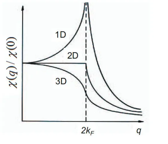
The bare (non-interacting) susceptibility for χ0ph(~q, ω) is shown in figure 1.7 for a free Fermi-gas is dimensions d=1,2 and 3 at T = 0. In d=1 this function diverges at a wave-vector ~q = 2~kF that connects points on opposite sides of the Fermi surface. This
divergence arises becauseσ,~k=σ,~k+~q over a finite domain in d=1. From the denomina-tor of equation 1.25 we can see that this will lead to a divergence inχ0ph(~q, ω), signaling an instability towards CDW order. This property thatσ,~k =σ,~k+Q~ over a finite domain
[image:39.596.145.433.425.672.2]is referred to as perfect nesting.
Figure 1.7: Bare particle-hole susceptibility, χ(q) = χ0ph(|~q|, ω = 0) for Fermi gas
in dimension d=1,2 & 3 at T = 0. The logarithmic divergence at q = 2kF in d=1
signifies a weak coupling instability to CDW order: the Peierls instability. Ind >1 the susceptibility is not divergent and there is no weak-coupling instability of the Fermi
Peierls recognised that, due to this perfect nesting, a one-dimensional metal would al-ways be unstable to distorting the lattice at wave-vector Q~ = 2~kF [39]. The decrease
in internal energy from opening a gap at the Fermi surface will always out-weigh the increase due to the lattice distortion. This weak-coupling instability (it exists for arbi-trarily small repulsive interactions) is known as the Peierls instability.
In d>1 the story is quite different. The perfect nesting condition is not fulfilled except in finely tuned circumstances. Consequently there is no divergence ofχ0ph(~q, ω) (as show for the free Fermi gas in figure 1.7) and no weak-coupling instability to CDW order, except under finely tuned conditions. This is to be contrasted with the particle-particle susceptibility which always diverges because, in the presence of time-reversal symmetry,
σ,~k = −σ,−~k. This can be viewed as another type of perfect nesting which persists to
arbitrary dimension. Thus the BCS superconducting instability is, in general, the only weak-coupling instability of the Fermi liquid.
The cuprate superconductors are quasi two-dimensional. For realistic Fermi surfaces, any CDW order in these materials requires a critical effective interaction strength between quasi-particles. Consequently the ordering temperature will depend on the strength of the effective interactions and the wave-vector will be influenced by any momentum de-pendence of the interaction. Extending equation 1.24 to an interaction with momentum dependence, a rough criterion for forming density wave order at wave-vector Q~ is that
g(~q)χ0ph(~q,0) = 1. In considering a mechanism for the formation of CDW in cuprates, it is important to keep in mind the importance of both the the Fermi surface (if one exists) and the interaction between its quasi-particles.
1.4
Unconventional Density Waves in Cuprates
CDW order has now been detected in several hole-doped cuprate compounds and would thus appear to be ubiquitous in cuprates. This in turn suggests that it is an intrinsic and generic property of doping holes into the CuO2 plane. However, its relationship to
the high-temperature superconductivity and pseudogap remains unclear.
The first detection of CDW in cuprates was made in a family of cuprates based on the insulator La2CuO4. In La2−x−yNdySrxCuO4+δ and La2−xBaxCuO4+δ, “stripe” order,
the relationshipQ~c= 2Q~s≈(14,0); (0,14), was detected by neutron scattering [40]. The
stripe order is strongest in the vicinity of hole-dopingp≈1/8 where there is an anoma-lous suppression in the bulk superconducting Tc, known as the “1/8th anomaly” [41].
The resonant x-ray scattering study of Abbamonteet al. characterised this stripe order as the segregation of holes in the CuO2 plane into regions of undoped antiferromagnetic
insulator separated by domain walls of holes [42].
Short-ranged CDW order was first detected in Bi2Sr2CaCu2O8+δ,
Bi2−yPbySr2−xLaxCuO6+δ and NaxCa2−xCuO2Cl2 by scanning tunnelling
mi-croscopy [43–46]. Advances in resonant x-ray scattering then led to the detection of short-ranged CDW order in YBa2Cu3O6+x, which was subsequently also detected by
hard x-ray diffraction [47–49]. Resonant x-ray scattering also confirmed the presence of CDWs in the bulk of Bi2Sr2CaCu2O8+δ and Bi2−yPbySr2−xLaxCuO6+δ with the same
wave-vectors as those detected by STM studies, as well as detecting short-range CDW order in HgBa2CuO4+δ [50].
The first hint of CDW order in YBa2Cu3O6+x was given by the observation of quantum
oscillations in YBa2Cu3O6+x whose frequencies correspond to small electron pockets
[51]. Quantum oscillations, also implying the existence of small electron pockets, were subsequently detected in Hg-1012 [52]. A reconstruction of the Fermi surface by a CDW was proposed as an explanation of these observations [53].
Developments in high magnetic field x-ray diffraction techniques are providing exciting new information about the cuprate CDW [54–56]. Pulsed field measurements utilising a free electron laser have detected the onset of a CDW in YBa2Cu3O6+x in applied
magnetic fields &15 T, with a correlation volume of ∼ 105 unit cells. This high-field CDW, which I will call CDW-II, appears distinct from the short-ranged charge order present at B=0, in that it is coherent along the direction perpendicular to the CuO2
planes with a periodicity of 1 unit cell. In contrast, the zero-field CDW shows very weak correlations along this direction, with a periodicity of≈2 unit cells.
Details of the experimental evidence for CDW order in cuprates is given in the appro-priate chapters throughout this thesis. A recent review can also be found in reference [58].
1.5
The Significance of CDW in Cuprates
Although they differ slightly in detail, the CDWs observed in the cuprates have several generic features. The wave-vector(s) are axial, meaning that they are along the Cu-O directions Q~x = (Q,0) and Q~y = (0, Q). At zero magnetic field the CDW order is
short-ranged with correlation length no longer than 2 wavelengths, except in the case of La2−xBa2CuO4+δ [58].
The CDW onset temperature forms a dome centered onp= 0.12 as shown in figure 1.5. At this doping there is an anomaly inTc(p) so that it either forms a local minimum or a
point of inflection, withTcin some materials being suppressed to very low temperatures
[59]. In others the effect is weaker at zero field, but the application of a magnetic field suppressesTcto zero at this doping, splitting the superconducting dome in two [60]. This
already suggests an intimate relationship between the CDW and superconductivity.
In 2002 Hoffman et al., using SI-STM, discovered halos of periodic conductance mod-ulations surrounding superconducting vortex cores in Bi2Sr2CaCu2O8+δ [45]. These
modulations, shown in figure 1.8 (a), are indicative of CDW order enhanced by the suppression of superconductivity.
Further evidence of a strong relationship between between superconductivity and CDW order is seen by x-ray scattering studies in a magnetic field. Figure 1.8 (b) shows data from Changet al on YBa2Cu3O6+x [49]. At zero magnetic field the scattering intensity
at the CDW wave-vector increases gradually with decreasing temperature, reaching a maximum at Tc and then decreasing again. The application of a magnetic field has
no effect on the scattering intensity above Tc but the intensity rapidly increases with
magnetic field below Tc. This is suggestive of a strong competition between CDW
formation and superconductivity.
Figure 1.8: (a)Approximately 4a0periodic tunnelling conductance modulations
sur-rounding superconducting vortex cores in Bi2Sr2CaCu2O8+δ, measured using SI-STM.
These suggest halos of enhanced CDW order forming due to the suppression of su-perconductivity. Reproduced from reference [45] with permission. (b) Temperature and magnetic field dependence of x-ray diffraction intensity at CDW wave-vectors in YBa2Cu3O6+x. With decreasing temperature, the scattering intensity onsets
gradu-ally at a temperature TCDW > Tc and rises to a maximum atTc for B=0T and then
decreases again. As a magnetic field is applied this decrease in scattering intensity is lessened and for the B=15 & 17 T data continues to rise throughTc and saturate.
phase of matter it is. It is clear that translational symmetry is broken but what of the point group symmetry? This would be broken in a stripe-like state with CDW alongQ~x
orQ~y but not both.
It is possible that experimental observations of CDW result from a state which breaks both translational and phase symmetry. This would be a superconductor that breaks translational symmetry, akin to that first proposed by Fulde, Ferrel, Larkin and Ovchin-nikov but in the absence of an applied magnetic field [61–63]. Certain forms of this “pair density wave” (PDW) order would also result in a CDW. This is because the density of Cooper-pairs, which are charged, is modulated. A PDW would offer a natural explana-tion of why the superconductivity and CDW are so strongly coupled to each other in cuprates.
The PDW is a state of matter which has never been directly detected. Establishing its existence in cuprate superconductors would be profound, not just within condensed matter physics but also in high-energy physics and astronomy where PDW states have been predicted to exist in dense quark matter [64].
There is still great interest and uncertainty in the nature of the cuprate pseudogap. It is natural to question the relationship between the charge order and the pseudogap. For instance, is the pseudogap caused by the CDW; either as a static or fluctuating entity? If not, then by what mechanism does the CDW form out of the pseudogap liquid? Key insights into this can be gained from examining the spectral function in the CDW and pseudogap regimes of the cuprate phase diagram.
Ultimately, given such a strong coupling between CDW and superconductivity, it is im-portant to establish the relationship between them. Is CDW order a necessary ingredient or consequence of a minimal model that describes high temperature superconductivity in cuprates? The goal of the research described in this thesis was to investigate issues such as this.
1.6
Organisation of this Thesis
Chapter 3 details the extension of SI-STM to image states of matter with non-trivial structure within the unit cell of a material.
In chapter 4 I describe utilising the techniques detailed in chapters 2 and 3 to characterise the CDW in Bi2Sr2CaCu2O8+δ and NaxCa2−xCuO2Cl2. I will show that the CDW in
these materials modulates a broken rotational symmetry within each unit cell. I will also present evidence that the CDW in cuprates has a tendency to break rotational symmetry globally as well as locally. The effects of the CDW on the electronic structure will also be discussed.
In chapter 5 I will outline the theoretical basis and development of nanometer resolution scanned Josephson tunnelling microscopy (SJTM) in cuprates. In chapter 6 I will de-scribe inhomogeneous superconducting states of matter known as “pair density waves”, as well as evidence and theoretical proposals for their existence in cuprates. In chap-ter 7 I will detail the use of SJTM to detect periodically modulated superconductivity in Bi2Sr2CaCu2O8+δ, the first direct detection of such a state in any superconductor.
Combining this with knowledge of the CDW from chapter 4 and other reported mea-surements, I will discuss the consequences of this for the cuprate phase diagram.
Spectroscopic-Imaging STM
(SI-STM)
In this chapter I detail the main experimental technique used in this thesis:
Spectroscopic-Imaging Scanning Tunnelling Microscopy (SI-STM). I outline the theoretical basis for its use as a tunnelling spectroscopy of
superconduc-tors as well as data analysis techniques specific to cuprate superconducsuperconduc-tors. I also give details of the cuprate samples studied.
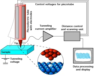
Scanning tunnelling microscopy (STM) is a technique which uses the tunnelling current of electrons between a sharp metal tip and a sample to image its surface [65]. An exponential dependence of the tunnelling current on the distance between tip and sample makes the STM very sensitive to small changes in surface topography, allowing atomic resolution imaging. STM can also act as a spectroscopic tool by using the tunnel junction between tip and sample to carry out tunnelling conductance spectroscopy, revealing information about the electronic states contributing to the tunnelling current. The advantage of performing spectroscopy with an STM is that it can be done with atomic resolution. The theoretical basis for the topographic and spectroscopic capabilities of STM are outlined in this chapter.
STM came to take a prominent role in the study of quantum matter with the advent of spectroscopic imaging STM (SI-STM) [27, 28]. In SI-STM the topographic and spectro-scopic abilities of the STM are systematically combined. The sample’s surface topogra-phy and spectroscopic information are obtained simultaneously across a two-dimensional
grid of points, or pixels. In doing so, one is essentially visualising the energy-resolved density of states of electrons in the material. In this chapter I will detail the techniques needed to obtain both real and momentum space information about the wave-functions in cuprate superconductors.
The rapid and fairly specialised development of the field means that for completeness I must touch on a fairly large number of sub-topics, some of which are fairly technical; one way to use this chapter might be to back-reference to it from the main results chapters of the thesis rather than try to take in every detail on first reading.
2.1
Quantum Tunnelling as a Spectroscopy
The experiments presented in this thesis rely on measuring the tunnelling current of electrons between a sample and a metal electrode across an insulating barrier [66, 67]. The tunnelling process consists of transferring an electron from a many-body state that is localised in the left electrode to another many-body state localised in the right electrode. Of course, by symmetry we expect the reverse process to have an equal rate, resulting in zero net current. However, under external application of a bias such as a current or voltage this symmetry is broken resulting in a net a current.
The variation of the current with the applied bias can yield information about the many-body states involved. Calculating the rates of these tunnelling processes from first principles is not generally possible. In the following section I will describe the tunnelling Hamiltonian formalism that can be used to extract spectroscopic information from the tunnelling current, without exactly solving the tunnelling problem [68, 69].
2.1.1 Tunnelling Hamiltonian Formalism
Within the tunnelling Hamiltonian formalism, the total Hamiltonian is given by
ˆ
H = ˆHL+ ˆHR+ ˆHT , (2.1)
where ˆHL and ˆHR describe the many-body states in the left and right electrodes
sep-arately, in the absence of each other [69]. ˆHT contains all additional terms that arise
An exact treatment of this problem for two interacting many-body states in the right and left electrodes is not generally analytically tractable. Instead, we can treat ˆHT
perturbatively. Typically we use a tunnelling Hamiltonian of the form,
ˆ
HT =
X
i,j
Mi,jˆc†L,iˆcR,j+Mj,i∗ cˆ
†
R,jcˆL,i
, (2.2)
where ˆc†L,i creates an electron in stateion the left electrode and ˆc†R,j creates an electron in statejon the right electrode [69]. I will now examine the consequences of this Hamil-tonian for various choices of the HamilHamil-tonians ˆHL and ˆHR corresponding to
Normal-Insulator-Normal (NIN), Normal-Insulator-Normal (SIN) and Superconductor-Insulator-Superconductor (SIS) tunnel junctions.
2.1.2 Normal - Insulator - Normal (NIN) Tunnelling
In the case of two normal metal electrodes the Hamiltonians are given by
ˆ
HL=
X
~ k
~kˆc†L,~kˆcL,~k (2.3)
ˆ
HR=
X
~ q
~qˆc
†
R,~qˆcR,~q (2.4)
ˆ
HT =
X
~k,~q
M~k,~qˆc†L,~kˆcR,~q+M~q,~∗kˆc†R,~qˆcL,~k
(2.5)
where ˆc†
L,~k creates an electron of crystal momentum
~
k in the left electrode with energy
kmeasured relative to the Fermi energy. Here, spin indices have been suppressed under
the assumption that no spin-flip processes take place in tunnelling.
We can then perturbatively calculate the current of electrons from the left to the right electrode using Fermi’s golden rule as
IL→R=
2πe
~
X
~k,~q
|M~k,~q|2f~k[1−fq~]δ(~k−~q) , (2.6)
wheref~k is the occupation number of the state~k. Similarly, the reverse current is given
by
IR→L=
2πe
~
X
~k,~q
with the net current from left to right given by I =IL→R−IR→L.
Under the simplifying assumption that T = 0 and the matrix elements, |M~k,~q|= |M|,
are a constant for states within eV of the chemical potential then this reduces to the form
I = 2πe
~
|M|2 Z eV
0
nL(+eV)nR()d , (2.8)
wheren() is the momentum integrated density of states at energy[69].
Under a further assumption that we choose a right hand electrode with a constant density of states nR(E) =nR(0), then equation 2.8 becomes
I = 2πe
~
|M|2nR(0)
Z eV
0
nL(+eV)d (2.9)
and nL(E) can be measured directly through the differential tunnelling conductance
dI dV =
2πe2
~
|M|2n
R(0)nL(eV) . (2.10)
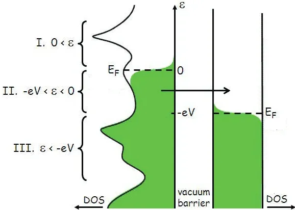
The physical tunnelling processes resulting in these equations are depicted in figure 2.1. Tunnelling may only occur from filled states to empty states. Hence by applying a positive bias we are probing the empty states of the left electrode (or sample) and with a negative bias its filled states.
The assumption of an energy independent matrix element, |M~k,~q|=|M|, is not in any
sense innocuous. For metals described by the independent-particle pictures used in equations 2.3 and 2.4, Harrison calculated the matrix elements M~k,~q within the WKB
approximation [71]. The conclusion was that the energy dependence of the matrix elements exactly cancels that of the density of states. This results in featureless, ohmic tunnellingI(V) curves.
Figure 2.1: Schematic of tunnelling from left hand electrode with negative bias
ap-plied, to right hand electrode. Green shading indicates filled states. Only energy ranges where left-hand states are filled and right-hand states are empty (i.e region II) contribute to the net tunnelling current. The right hand density of states (DOS) is drawn flat as is required if useful spectroscopic information is to be obtained without
deconvolution. Figure adapted from reference [70].
2.1.3 Superconductor-Insulator-Normal (SIN) Tunnelling
Now I will discuss tunnelling between a normal metal and a superconductor. This is the configuration of electrodes used in the STM studies of cuprate superconductors in chap-ter 4, where a tungsten tip is used to perform spectroscopy on cuprate superconductor samples. In this case the normal and superconducting electrode Hamiltonians, ˆHN and
ˆ
HS, are given by
ˆ
HN =
X
~ q
~qˆc
†
L,~qˆcL,~q (2.11)
ˆ
HS=
X
~k
E~k( ˆα
†
~kαˆ~k+ ˆβ~kβˆ
†
~k) (2.12)
(2.13)
where
α~k =u~kˆcR,~k,↑−v~kcˆ†R,−~k,↓ (2.14)
β~k=u~kcˆR,−~k,↓+v~kˆc
†