Electro-optic modulation in bulk silicon using surface
plasmon resonance
Kapil Debnath
1, Pedro Damas
2, Liam O’Faolain*
SUPA, School of Physics & Astronomy, University of St Andrews, North Haugh,
St Andrews KY16 9SS, UK
*Corresponding author:
[email protected]
1 Nano Research Group, Faculty of Physical Sciences and Engineering, University of Southampton,
Southampton, SO17 1BJ, UK, email: [email protected]
2 Institut d’Electronique Fondamentale, Univ. Paris Sud, CNRS UMR 8622, 91405 Orsay, France, email:
Abstract
We propose and present simulated results for a new design of an optical modulator based on Surface Plasmon Polariton (SPP) resonance. The modulator is realized on a bulk silicon substrate, thus offering an opportunity for front-end integration with electronic circuits. The device consists of a dielectric waveguide evanescently coupled to a SPP mode at the interface between bulk silicon and metal. By using SPP resonance we achieved an ultra-high spectral sensitivity (~5000nm/refractive index unit) with large modulation bandwidth (90nm). For a refractive index change of 0.02, we achieved 100nm shift in resonance wavelength and a modulation depth of ~10dB.
Keywords: Surface plasmons, Integrated optoelectronic circuits, Modulators, Silicon photonics
1. Introduction
As the clock speed and wiring density in microprocessors continues to rise, various problems associated with metallic interconnects are becoming increasing difficult to resolve [1-3]. The limited capacity of electrical interconnects is becoming a major problem not only for backplanes and communication between boards, but also for shorter distances, such as between chips and even on-chip [4]. The physical advantages of optics over electrical signals for interconnections has heralded the emergence of the optical interconnect. Unlike an electrical wire, the limit on data transmission in an optical waveguide can be as high as 100Tbit/s and data transfer at high bit rates is much more energy efficient. At the same time, the possibility of integrating both electronics and photonics on the same platform gave rise to the field of silicon photonics [4, 5].
Silicon on insulator (SOI) wafers comprising of a thick buried oxide (BOx) layer have become the most popular platform for monolithic integration of silicon photonic devices with passive optical components including ultra-low loss waveguides [6] and active optical components such as high speed electro-optic modulators [7] and photodetectors [8]. However, on cost and performance grounds, bulk silicon is used in most electronic applications, such as microprocessors, high volume and high density memories etc. BOx layers are generally avoided in bulk silicon devices, as they would act as heat traps and lead to a reduction in the integration density. Therefore, in order to replace electrical interconnects with integrated photonic links for intra-chip and inter-chip
communications, photonic components need to be integrated with CMOS devices on bulk silicon [9].
2. Prior art and device design
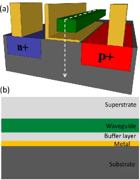
our design is shown in Fig. 1(a). The cross sectional view is shown in Fig. 1(b). In this design the light is guided between bulk silicon and metal layer and thus obviates the need for any bottom cladding layer and achieve integration on the same plane. This implementation is remarkably simple allowing front-end integration with minimal changes to the CMOS processes currently in use. In this
configuration, light propagating through the dielectric waveguide in a transverse magnetic (TM) mode evanescently couples to the SPP mode existing at the interface of the metal and bulk silicon. The coupling wavelength is decided by the intersection of the dispersion curves of the waveguide mode and the SPP mode, i.e. where both the modes are phase matched. By altering the refractive index of the silicon (e.g. by using free carrier plasma dispersion effect) we can achieve modulation at the coupling wavelength, and thus get modulation in the output intensity of the waveguide.
Fig. 1. (a) Schematic of the proposed SPP resonance based modulator. The structure can be embedded in a p-i-n junction as shown and the SPP resonance wavelength can be modulated using free carrier plasma dispersion effect. (b) A cross sectional view of the device. The SPP mode exists at
the metal-silicon interface. The dielectric waveguide mode couples evanescently to the SP mode through the buffer layer.
3. Simulation and results
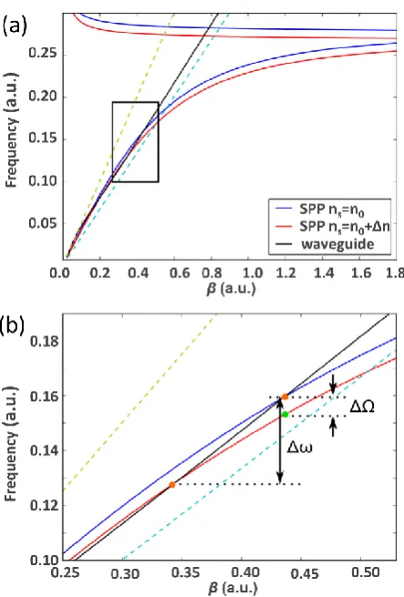
It is known that in refractive index sensors extraordinarily high spectral sensitivity can be achieved using SPP modes [12]. The spectral sensitivity of such sensors can be more than 104nm/RIU. When
[image:3.595.187.410.246.533.2]dielectric waveguide. At a certain propagation constant (β), the frequency (f) shift of the surface plasmon mode has a spectral sensitivity comparable with those relying on a conventional resonant cavity scheme (ΔΩ). However, since the position of the resonance dip is determined by the
intersection between the dispersion curves of the SPP mode and waveguide mode, the new resonance dip is located at a frequency associated with a different SPP mode with a different propagation constant, thus resulting in a frequency shift of Δω>>ΔΩ,. This results in a large spectral sensitivity.
Fig. 2. (a) Dispersion relations of the waveguide mode, SPP modes with and without modified refractive index of the dielectric layer are shown in black, red and blue curves respectively. The dashed lines represent the light lines of the dielectric waveguide core and cladding. (b) Section of
the dispersion relation highlighted by the black rectangle in Fig. 2(a). The orange dots show the phase matching points between two arbitrary waveguide (black) and SPP (red and blue) modes dispersion relations, whereas, the green dot shows the shift in frequency for the same propagation
constant of the SPP mode. When a small change is induced in the refractive index of the dielectric layer, a large shift in the coupling (or phase-matching) wavelength is observed, i.e. Δω>>ΔΩ. Here we exploit this extraordinary sensitivity inherent to SPP in the other way round: instead of sensing a change in ∆n, one can induce a change ∆λ in the coupling wavelength by properly changing ∆n underneath the metal. The design is carried out using MEEP a freely available finite difference time domain (FDTD) simulation software [13]. We first analytically estimate the phase matching condition needed in order to couple light from the waveguide to the SPP, around the
[image:4.595.186.408.177.505.2]compatibility issues. The choice of materials for remaining layers (i.e. waveguide, buffer and superstrate) primarily depends on the effective index of the SPP mode at around 1550nm
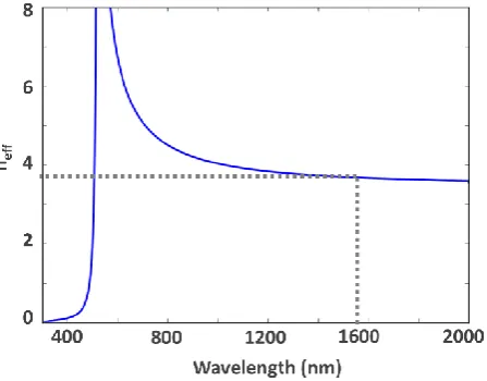
[image:5.595.187.411.138.313.2]wavelength. The dispersion relation of the SPP mode at the Si-Cu interface is calculated using the Drude-Lorentz model [14] and is shown in Fig. 3.
Fig. 3. Effective index of the SPP mode at the Si–Cu interface. The grey dashed line highlights the effective index of the waveguide required for coupling around the C-band of the telecomm
wavelength.
The dispersion relation suggests that in order to couple light to the SPP mode around 1550nm wavelength, the effective index of the dielectric waveguide mode should be close to 3.68 to ensure phase matching condition between SPP and waveguide mode. In order to achieve such high effective index we chose the waveguide refractive index to be 4.1 and for buffer and superstrate layer we chose silicon nitride (Si3N4) with refractive index of 2. Although there are not many materials available with such high refractive index in telecomm wavelength, it has been shown that with complete amorphization, amorphous-silicon can reach refractive index of 4 [15]. Here we chose the metal layer thickness of 50nm, the waveguide thickness of 370nm and the buffer layer thickness of 150nm. For these dimensions the effective index of the fundamental TM mode in the waveguide has an effective index of 3.63, which corresponds to a coupling wavelength near 1600nm.
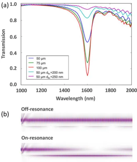
Fig. 4. (a) Transmission spectra of the device for different device length and buffer layer thickness. dBL is the buffer layer thickness. (b) Magnetic field profile at wavelengths far from the resonance
(1500nm) and at resonance respectively (1602nm).
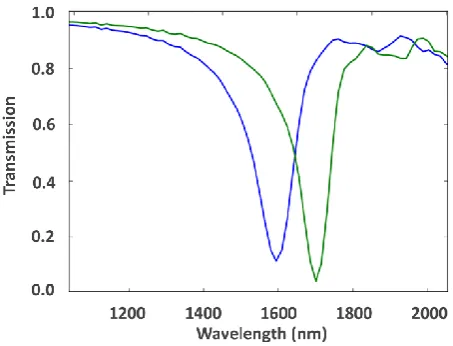
[image:6.595.184.409.71.338.2]Fig. 5. Transmission spectra when the bulk silicon refractive index is 3.47 (blue) and 3.45 (green). For a refractive index change of 0.02, the resonance wavelength shifts by 100nm.
4. Conclusion
In conclusion, we have proposed an optical modulator design based on SPP resonance due to evanescent coupling between a dielectric waveguide mode and SPP mode at the bulk silicon-metal interface. The proposed design is completely CMOS compatible and offers an easy route for front-end opto-electronic integration. Besides the obvious advantage of compatibility, the use of SPP resonance also provides ultra-high spectral sensitivity with a large modulation band-width. These characteristics are very hard to find in any optical modulator implemented so far, and gives this modulator design an enormous potential for future applications in silicon photonics and overcomes many of the limitations of modern optical modulators and communications.
Acknowledgement
The authors acknowledge funding from the EPSRC in the UK under the UK Silicon Photonics project.
References
1. R. Ho, K.W. Mai, and M.A. Horowitz, The future of wires, Proc. of the IEEE 89 (2001) 490-504. 2. D.A.B. Miller and H.M. Ozaktas, Limit to the Bit-Rate Capacity of Electrical Interconnects from the Aspect Ratio of the System Architecture, J. of Parallel and Distributed Computing 41 (1997) 42-45. 3. D.A.B. Miller, Rationale and challenges for optical interconnects to electronic chips, Proc. of the IEEE 88 (2000) 728-749.
4. D. A. B. Miller, Device Requirements for Optical Interconnects to Silicon Chips, Proc. of the IEEE 97 (2009) 1166-1185.
6. J. Cardenas, C. B. Poitras, J. T. Robinson, K. Preston, L. Chen, and M. Lipson, Low loss etchless silicon photonic waveguides, Opt. Exp. 17 (2009) 4752-4757.
7. D. J. Thomson, F. Y. Gardes, J.-M. Fedeli, S. Zlatanovic, Y. Hu, B. P. P. Kuo, E. Myslivets, N. Alic, S. Radic, G. Z. Mashanovich, G. T. Reed, 50-Gb/s silicon optical modulator, IEEE Photon. Technol. Lett. 24 (2012) 234-236.
8. D. Marris-Morini, L. Virot, C. Baudot, J.-M. Fédéli, G. Rasigade, D. Perez-Galacho, J.-M. Hartmann, S. Olivier, P. Brindel, P. Crozat, F. Bœuf, and L. Vivien, A 40 Gbit/s optical link on a 300-mm silicon platform, Opt. Exp. 22 (2014) 6674-6679.
9. C. Sun, M. Georgas, J. Orcutt, B. Moss, Y. Chen, J. Shainline, M. Wade, K. Mehta, K. Nammari, E. Timurdogan, D. Miller, O. Tehar-Zahav, Z. Sternberg, J. Leu, J. Chong, R. Bafrali, G. Sandhu, M. Watts, R. Meade, M. Popović, R. Ram, and V. Stojanović, A monolithically-integrated chip-to-chip optical link in bulk CMOS, IEEE J. Solid state circuits 50 (2014) 828-844.
10. A. Biberman, K. Preston, G. Hendry, N. Sherwood-Droz, J. Chan, J. S. Levy, M. Lipson, and K. Bergman, Photonic network-on-chip architectures using multilayer deposited silicon materials for high-performance chip multiprocessors, ACM J. Emerg. Technol. 7 (2011) 1.
11. K. K. Mehta, J. S. Orcutt, J. M. Shainline, O. Tehar-Zahav, Z. Sternberg, R. Meade, M. A. Popović, and R. J. Ram, Polycrystalline silicon ring resonator photodiodes in a bulk complementary metal-oxide-semiconductor process, Opt. let. 39 (2014) 1061-1064.
12. I. M. White and X. Fan, On the performance quantification of resonant refractive index sensors, Opt. Exp. 16 (2008) 1020-1028.
13. A. F. Oskooi, D. Roundy, M. Ibanescu, P. Bermel, J. D. Joannopoulos, and S. G. Johnson, MEEP: A flexible free-software package for electromagnetic simulations by the FDTD method, Comput. Phys. Commun. 181 (2010) 687-702.
14. A. D. Rakić, A. B. Djurišić, J. M. Elazar, and Marian L. Majewski, “Optical properties of metallic films for vertical-cavity optoelectronic devices,” Appl. Opt. 37 (1998) 5271-5283.
15. R. Loiacono, G. T. Reed, G. Z. Mashanovich, R. Gwilliam, S. J. Henley, Y. Hu, R. Feldesh, and R. Jones, Laser erasable implanted gratings for integrated silicon photonics, Opt. Exp. 19 (2011) 10728-10734.