Abstract—Hybrid optical-electronic NoC (HONoC) are recently considered as a promising solution to construct the low diameter and high energy efficiency network by introducing nano-photonic technologies. The traditional fully covered HONoC provides both electrical and optical links to all the nodes. Although extremely high bandwidth can be provided, large scale optical links necessitate too many wavelengths and moriorings, thus resulting in large static power. This over provision of bandwidth leads to ultra-low energy efficiency of the whole network. To solve the problem, we proposed hybrid optical-electronic mesh-based grouped NoC (HOG-NoC). HOG-NoC first interconnects the nodes with electrical mesh network, and then groups all the nodes into clusters. Each cluster has one optical interface. The optical nodes are further divided into four groups to decrease the utilized wavelengths and moriorings. Experiments showed that, compared to E-Mesh with 64 nodes under random traffic pattern, HOG-NoC improved throughput by 25.7%, decreased latency by 75% and reduced energy consumption by 12.9%.
Index Terms—HOG-NoC, hybrid NoC, Mesh-based, Grouped
I. INTRODUCTION
ith the development of the integrated circuit technique, the number of available transistors on a single chip is increasing larger and larger. As a consequence, more and more cores are integrated on the chip [1]-[2], which leads to the result that traditional interconnection no longer satisfies the communication requirement of multiprocessor System-on- Chip (MPSoC), because of critical issues such as poor scalability, limited bandwidth, the difficulty of parallelism communication and crosstalk [3]. Network-on-Chip (NoC) emerges as a new on-chip communication system to relieve these issues of MPSoC by using modern communication and network theories, which use routers as key component, providing better performance. However, large scale NoC may need long wires for global interconnects to reduce network diameter [4]. But long wires will no longer satisfy the communication needs because as
Manuscript received June 28, 2017. This work was supported in part by the National Natural Science Foundation of China (61376025) and the Natural Science Foundation of Jiangsu Province (BK20160806).
X. Yue is with the Collage of Electronic and Information Engineering, Nanjing University of Aeronautics and Astronautics, Nanjing, 211106, China.(email: [email protected]).
F. Ge and N. Wu is with the College of Electronic and Information Engineering, Nanjing University of Aeronautics and Astronautics, Nanjing, 211106, China (e-mail: [email protected]).
G. Yan is with the College of Electronic and Information Engineering, Nanjing University of Aeronautics and Astronautics, Nanjing, 211106, China, and with the College of Mathematics, Physics and Information Engineering, Anhui Science and Technology University, Fengyang, 233100, China.
semiconductor technologies continually shrink feature sizes and the frequency of the cores are increasing to gigahertz frequency range, metallic interconnects gradually become the bottleneck of NoC performance due to the limited bandwidth, long delay, large area, and high power dissipation [5]. In fact, 256-node Electrical Mesh NoC in 22nm CMOS technology has exceeded the allocated network power budget by an order of magnitude [6].
With the maturity of integrated silicon-compatible nano-photonic technologies, Optical Network-on-Chip (ONoC) are getting focused. ONoCs utilize light as the signal propagation medium of the network, which are tending to provide high bandwidth, low latency, low power and low electro-magnetic interference [7]. Moreover, wavelength division multiplexing (WDM), which enables many wavelengths to transmit data on a single waveguide, expands bandwidth largely. However, optical interconnects also have constrains. Firstly, wavelength number are limited because WDM technology is not mature enough, the most advanced dense wavelength division multiplexing enable limited wavelengths to work together, which constrains the scale of ONoC. Secondly, static energy consumption in ONoC is large and too many optical nodes will consume a large amount of energy [8]. What’s worse, small hops communication in ONoC, such as one hop communication, may consume more power and delay than ENoC, and also occupy the bandwidth of optical link. For instance, all optical NoC Amon proposed by Werner et al. [9] and QuT proposed by Hamedani et al. [10] although get better scalability by grouping, still fully covered optical nodes bring large static power consumption and provide no electrical connection for neighbored nodes, which leads to larger delay.
As a result, electronic interconnect will perform better in short-distance communication while optical interconnect fits for long distance communication. Make full use of the advantages of both electronic network and optical network will be a wise choice, that is, constructing a HONoC is promising to bring up with a better performance in delay, throughput and power consumption. In this way, optical links take the place of long wires in traditional NoC to provide better performance with lower energy loss.
Li et al. [5] has proposed a Hierarchical Cluster-based Optical NoC architecture HCONoC, in which optical interconnects are made up with many levels of cluster. In this architecture, neighbor nodes in different cluster will have to go optical layer although very close physically, bringing larger delay and energy consumption. Ye et al. [11] has proposed a Torus-based Hierarchical ONoC THOE, in which optical interconnect uses circuit switch to transmit data. Circuit switch need network to set up a path before transmission and tear down after transmission, which will
HOG-NoC: Hybrid Optical-Electronic
Mesh-based Grouped NoC
Xinxin Yue, Fen Ge, Ning Wu, Gaizhen Yan
impose large delay due to these two procedures are performed in electronic network, while the optical transmission procedure cost little delay. As a consequence, circuit switch fits for the case only when the packet is large, such as 1KB size and even more, which is uncommon in on-chip communication. Vantrease et al. [12] designed Corona for 256 nodes, in which cores are divided into 64 four-core cluster and they are connected with all-optical high-bandwidth DWDM crossbar. But critical difficulties occur when expanding the scale because wavelengths utilized at the same time are limited.
The existing network has promoted the development of hybrid network, but problems exist. Firstly, cluster-based electrical network did a bad job in neighbor communication because of unconnection. Secondly, circuit switching costs too much time to set up and tear down the path, which means high frequency and small data communications will suffer from this. Thirdly, global wavelength division optical crossbar limits the scale of the network.
Based on the above observation, we proposed a hybrid mesh-based NoC for MPSoC, which is called HOG-NoC. It is composed of an electrical interconnection layer and an optical layer where WDM is utilized, and we connect each layer with TSV (through-silicon via) [13]. We design the electrical interconnection layer as normal 2D mesh architecture, for the sake of providing electrical connection for any two neighbored nodes. In order to decrease the utilized wavelengths and moriorings, we divide the optical nodes into four groups. Besides, to deliver global communication and local communication in optical link and electronic link, respectively, we give out our routing algorithm to determine the routing path for each packet.
The rest of this paper is organized as follows. Section II describes proposed architecture and optimization. Section III introduces the routing mechanism. Experimental results of HOG-NoC will be compared with other NoCs in section IV. Section V is the conclusion of this paper.
II. ARCHITECTURE OF THE PROPOSED HOG-NOC A. Proposed Architecture
The proposed hybrid optical-electronic architecture is shown in Fig. 1. It consists of three layers: Electric Die, Electro-Optical Transceiver Die and Optical Die, as shown in Fig. 1(a). The Optical Die consists of waveguide for delivering packets in light and optical router which is made up with passive micro-rings for routing packets during transmission. And each optical node is allocated with a particular wavelength 𝜆𝑛 for routing address. The
Underneath layer is an Electro-Optical Die, which is composed of modulators and Photo-detectors for conversion between electrical and optical signal. The bottom layer is an electrical Mesh layer, in which main components are processor elements and electrical routers, as shown in Fig. 1(c), closed to heat sink for better thermal dissipation. Each Die is connected with TSVs for data transmission, as shown in Fig. 1(b).
In order to reduce optical nodes number and provide optical connection for each electrical node, we place an optical node every two hops in both X and Y direction. But traditional even distribution of optical nodes doesn’t serve
well for edge electrical nodes because not all edge nodes can access optical nodes within one hop while edge nodes are more likely need to access optical nodes. In order to improve this problem, we firstly divide electrical nodes into four sub-meshes and optical nodes are placed close to the edge of network to serve for long-hops packets better within a sub-mesh with even number of nodes (such as a sub-mesh with 4 × 4 or 6 × 6 nodes). Within a sub-mesh with odd number of nodes (such as a sub-mesh with 5 × 5 nodes or 7 × 7 nodes), optical nodes are distributed in the center of each sub-mesh for fairness. Optical nodes distribution of a 8 × 8 network is shown as Fig. 1(c).
For each packet, it can choose to go electrical interconnect or optical interconnect for less delay or less energy consumption. When it goes optical layer, the source optical node will modulate data in the same wavelength with destination, then with the resonation of micro-rings in optical router, light with packet data will route toward destination optical node directly in a MWSR crossbar.
B. The Design of Optical Interconnection
With the scale of network increasing larger, more optical nodes and wavelengths are needed in the optical layer, in order that each optical node can be addressed when routing. But the number of wavelengths utilized in optical interconnect are limited because laser technology is not mature enough. On the other hand, power consumption of laser sources accounts for a large proportion in total power consumption in optical layer. Laser power is determined by
(a)
(b)
[image:2.595.330.543.55.374.2](c)
Fig. 1 Architecture of proposed HONoC. (a) The Architecture
the biggest insertion loss in the network, which is proportional to diameter of the network.
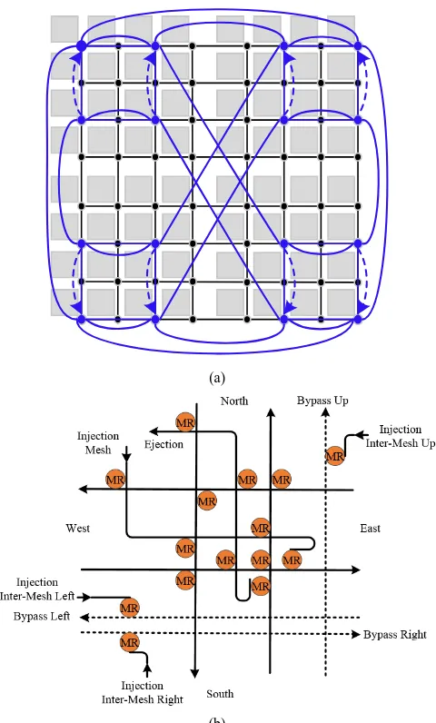
In order to reduce wavelength utilization and shorten diameter of the network, we separated optical nodes into four groups and each group is a sub-mesh, as shown in Fig. 2(a). In this occasion, number of optical nodes need to be a × a × 4 (a>=2). Within a sub-mesh, each optical node is assigned with a unique wavelength for addressing, and each node is connected with Mesh links, which are represented as straight lines within the sub-mesh in Fig. 2(a). Besides Mesh links, there are three bypass links alongside each node, and they are connected to the other three sub-meshes separately. In Fig. 2(a), bypass links are represented as curves within the sub-mesh and lines between different sub-meshes, and bidirectional bypass links are represented as solid lines while unidirectional bypass links are represented as dotted lines.In this way, communication between optical nodes within a sub-mesh starts at an Injection Mesh port and transfers with inner-mesh links through X-Y static routing algorithm. And for optical nodes distributed in different sub-meshes, communication will starts at an inner-mesh injection Mesh port and continues through bypass inter-mesh waveguides, which converge with Mesh links at destination sub-mesh. After that, X-Y static routing algorithm will be carried on for
addressing target optical node. The optical router used in HOG-NoC left up sub-mesh is shown as Fig. 2(b), and mirror structure will be used in other sub-meshes. Because of no confliction between inner-mesh and inter-mesh links, the four sub-meshed share the same wavelength sets to reduce wavelength utilization to 1/4, and by return this reduce large number of microrings and increases the scalability of the network greatly, especially when scale of network is large. On the other hand, since optical links have provided pretty large bandwidth for the network comparing with E-Mesh, we decrease the number of virtual channels of electrical routers in electrical layer of HOG-NoC to reduce redundant energy consumption of electrical buffers.
Anyway, conflicts happen in optical interconnect of HOG-NoC when many source optical nodes are sending to one destination node. In order to avoid conflicts, an all-optical MWSR is used as CN (Control Network).
III. ROUTING MECHANISM
For each packet generated, two paths can be selected toward destination including electrical path and optical path. In order to decrease power consumption of the network, route selection should be determined by power consumption calculation of different paths.
Assuming network scale is m × m, and each node is identified as 𝑁𝑖. For a packet transferred from source node 𝑛𝑠
to destination node 𝑛𝑑, the Manhattan Distance L between
𝑁𝑠 and 𝑁𝑑 can be calculated as equation (1).
𝐿 = |𝑛𝑑%m − 𝑛𝑠%m| + |𝑛𝑑/m − 𝑛𝑠/m| + 1 (1) If the packet is routing in electrical layer, power dissipation from 𝑁𝑠 to 𝑁𝑑 can be evaluated as equation (2)
where 𝑃𝑟and 𝑃𝑙 are power dissipation of electrical router and
global link transmit 1-bit data, respectively, and 𝐿𝑃 is packet
length.
𝑃𝐸= (𝑃𝑟× 𝐿 + 𝑃𝑙× (𝐿 − 1)) × 𝐿𝑃 (2) If the packet is transmitted in optical layer, routing path contains both electrical and optical path. Total power dissipation can be expressed as equation (3), where 𝑃𝐸𝑝 and
𝑃𝑂𝑝 are power dissipation of electrical part and optical part.
𝑃𝑂= 𝑃𝐸𝑝+ 𝑃𝑂𝑝 (3)
Power consumption of electrical part can be evaluated as equation (4) where 𝐿𝑠is Manhattan Distance between 𝑁𝑠 and
closest optical node, and 𝑁𝑑 is Manhattan Distance between
𝑁𝑑 and closest optical node.
𝑃𝐸𝑝= ((𝑃𝑟+ 𝑃𝑙) × (𝐿𝑠+ 𝐿𝑝+ 2)) × 𝐿𝑃 (4) Power consumption of optical part can be evaluated as equation (4) where 𝑃𝐸𝑂 and 𝑃𝑂𝐸 are power dissipation of
electro-optical and optical-electronic conversion for 1-bit data.
𝑃𝑂𝑝= (𝑃𝑂𝐸+ 𝑃𝐸𝑜) × 𝐿𝑃 (5) When 𝑃𝐸< 𝑃𝑂, the packet will be transmitted in electrical layer with X-Y static routing algorithm. Otherwise if 𝑃𝐸> 𝑃𝑂, the packet will be sent to closest optical node. Then packet will be injected into optical waveguide for propagation through one particular injection Mesh port according to destination sub-mesh. If destination node shares the same sub-mesh with source node, Injection Mesh port will be used. Otherwise, Injection Inter-Mesh Left, Injection Inter-Mesh
(a)
[image:3.595.52.292.59.457.2](b) Fig. 2 Architecture of HOG-NoC
Right and Injection Inter-Mesh up ports will be used according to destination location. After optical transmission, again X-Y static routing algorithm will be used for targeting destination.
In this way, routing choice is considered basing on power consumption calculation in each route. But when workload is
heavy, more situations should be considered to promote performance of the network. Optimizing routing mechanism to promote performance is left as future work.
IV. EXPERIMENT AND RESULT
[image:4.595.57.270.54.346.2]In order to evaluate the throughput, delay and energy of HOG-NoC, we implemented three networks including
Fig. 3 Throughput comparison for 64 nodes and 100 nodes under Random traffic pattern
0 0.1 0.2 0.3 0.4 0.5 0.6
0 0.1 0.2 0.3 0.4 0.5 0.6
Thro
u
g
h
p
u
t
(f
lits/co
re/cy
cle)
Injection Rate (flits/core/cycle) E-Mesh
O-Mesh HOG-NoC
0 0.1 0.2 0.3 0.4 0.5 0.6
0 0.1 0.2 0.3 0.4 0.5 0.6
Thro
u
g
h
p
u
t
(f
lits/co
re/cy
cle)
Injection Rate (flits/core/cycle) E-Mesh
[image:4.595.311.525.58.349.2]O-Mesh HOG-NoC
Fig. 4 Throughput comparison for 64 nodes and 100 nodes under Transpose1 traffic pattern
0 0.1 0.2 0.3 0.4 0.5 0.6
0 0.1 0.2 0.3 0.4 0.5 0.6
Thro
u
g
h
p
u
t
(f
lits/co
re/cy
cle)
Injection Rate (flits/core/cycle) E-Mesh
O-Mesh HOG-NoC
0 0.1 0.2 0.3 0.4 0.5 0.6
0 0.1 0.2 0.3 0.4 0.5 0.6
Thro
u
g
h
p
u
t
(f
lits/co
re/cy
cle)
Injection Rate (flits/core/cycle) E-Mesh
[image:4.595.318.545.381.665.2]O-Mesh HOG-NoC
Fig. 5 Latency comparison for 64 nodes and 100 nodes under Random traffic pattern
0 50 100 150 200
0 0.1 0.2 0.3 0.4 0.5 0.6
Latency
(cy
cles)
Injection Rate (flits/core/cycle) E-Mesh
O-Mesh HOG-NoC
0 50 100 150 200
0 0.1 0.2 0.3 0.4 0.5 0.6
Latency
(cy
cles)
Injection Rate (flits/core/cycle) E-Mesh
O-Mesh HOG-NoC
Fig. 6 Latency comparison for 64 nodes and 100 nodes under Transpose1 traffic pattern
0 50 100 150 200
0 0.1 0.2 0.3 0.4 0.5 0.6
Latency
(cy
cles)
Injection Rate (flits/core/cycle) E-Mesh
O-Mesh HOG-NoC
0 50 100 150 200
0 0.1 0.2 0.3 0.4 0.5 0.6
Latency
(cy
cles)
Injection Rate (flits/core/cycle) E-Mesh
[image:4.595.60.286.386.675.2]E-Mesh, O-Mesh and our hybrid optical-electronic HOG-NoC for 64 nodes and 100 nodes under both random traffic pattern and transpose1 traffic pattern in cycle-accurate NoC simulation environment JADE [14]. In the experiment, packet size was set as 128 bits and energy evaluation was based on 45nm DESENT [15] power model.
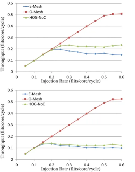
A. Throughput
Throughput results comparison of three networks is shown in Fig. 3 and Fig. 4. Under Random traffic pattern, E-Mesh, O-Mesh and HOG-NoC get saturated at injection rate of 0.35, 0.5 and 0.45 for 64 nodes and get saturated at injection rate of 0.3, 0.5 and 0.35 for 100 nodes, respectively. Under Transpose1 traffic pattern, E-Mesh, O-Mesh and HOG-NoC get saturated at injection rate of 0.2, 0.5 and 0.25 for 64 nodes and get saturated at injection rate of 0.15, 0.5 and 0.15 for 100 nodes, respectively. Compared with E-Mesh, HOG-NoC improved saturated throughput by 25.7% and 16.55% for 64 nodes and 100 nodes under Random traffic pattern, and improved saturated throughput by 16.9% and 4.4% for 64 nodes and 100 nodes under Transpose1 traffic pattern. O-Mesh had the best throughput because of all-optical interconnect provides extra-high bandwidth.
B. Latency
Latency results comparison is shown in Fig. 5 and Fig. 6. It can be seen that, saturated latency of proposed HOG-NoC has been reduced by 75% and 64% for 64 nodes and 100 nodes under Random traffic pattern and by 69% and 18% for 64 nodes and 100 nodes under Transpose1 traffic pattern compared to E-Mesh. Injection rate for 100-cycle latency of HOG-NoC has been extended by about 20% and 22% for 64 nodes and 100 nodes under Random traffic pattern and by about 6% and 18% for 64 nodes and 100 nodes under Transpose1 traffic pattern compared with E-Mesh. Latency of O-Mesh keeps lower than the other two networks because of direct optical link connection for each node.
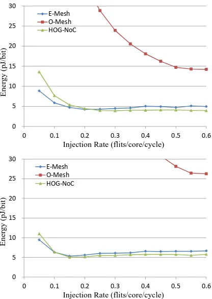
C. Energy Efficiency
Energy efficiency comparison results are shown in Fig. 7 and Fig. 8. Compared with E-Mesh and O-Mesh, HOG-NoC reduces per-bit energy consumption by 12.9% and 84% for 64 nodes and by 22.6% and 91% for 100 nodes under Random traffic pattern when network gets saturated, respectively. Under Transpose1 traffic pattern, HOG-NoC reduces per-bit energy consumption by 8% and 86% for 64 nodes and by 5% and 94% for 100 nodes compared with E-Mesh and O-Mesh. Energy efficiency of HOG-NoC is smaller than E-Mesh when injection rate is light, because static power consumption accounts for large proportion in total power consumption of optical layer.
Although O-Mesh shows better throughput and delay, per-bit energy consumption is extremely high than HOG-NoC, because O-Mesh has bigger network diameter and a pretty larger number of micro-rings caused by more wavelengths occupation. As a result, energy efficiency of O-Mesh is unaffordable for chips.
D. Area
[image:5.595.63.274.57.353.2]In HOG-NoC, we introduce an additional optical layer for better performance compared to E-Mesh. As a result, in electrical layer electrical routers connected with optical layer will introduce another port for data transmission with optical routers, which increases area cost of the network. Since optical layer has provided pretty high bandwidth, we decrease the number of virtual channels of electrical router for reducing energy cost and area cost, which amortizes the area cost caused by additional port of electrical routers. DSENT evaluation shows that area cost of electrical routers
Fig. 7 Energy comparison for 64 nodes and 100nodes under Random traffic pattern
0 5 10 15 20 25 30
0 0.1 0.2 0.3 0.4 0.5 0.6
Ener
g
y
(pJ
/b
it)
Injection Rate (flits/core/cycle) E-Mesh
O-Mesh HOG-NoC
0 5 10 15 20 25 30
0 0.1 0.2 0.3 0.4 0.5 0.6
Ener
g
y
(pJ
/b
it)
Injection Rate (flits/core/cycle) E-Mesh
O-Mesh HOG-NoC
Fig. 8 Energy comparison for 64 nodes and 100nodes under Transpose1 traffic pattern
0 5 10 15 20 25 30
0 0.1 0.2 0.3 0.4 0.5 0.6
Ener
g
y
(pJ
/b
it)
Injection Rate (flits/core/cycle) E-Mesh
O-Mesh HOG-NoC
0 5 10 15 20 25 30
0 0.1 0.2 0.3 0.4 0.5 0.6
Ener
g
y
(pJ
/b
it)
Injection Rate (flits/core/cycle) E-Mesh
[image:5.595.64.272.387.680.2]was reduced by 33% because of decreased virtual channels. With the maturity of 3D integrating technology, optical layer can be integrated as a single layer above electrical layer, which will not introduce additional area cost.
V. CONCLUSION
In this paper, we proposed hybrid optical-electronic Network-on-Chip HOG-NoC. Experiment shows that HOG-NoC improved throughput by 25.7% and 16.55%, and reduced latency by 75% and 64% at most compared to E-Mesh for 64 nodes and 100 nodes under Random traffic pattern, respectively. And HOG-NoC reduced energy consumption by 12.9% and 84% for 64 nodes, by 22.6% and 91% for 100 nodes under Random traffic pattern compared with E-Mesh and O-Mesh when get saturated. As a conclusion, HOG-NoC provides better performance with lower energy cost comparing with E-Mesh, which only introduces one optical layer with 3D integrating overhead.
REFERENCES
[1] Horowitz, M. and W. Dally. “How scaling will change processor architecture”. Solid-State Circuits Conference, 2004. Digest of
Technical Papers. ISSCC. 2004 IEEE International.
[2] Bell, S., B. Edwards, J. Amann, et al. “TILE64 - Processor: A 64-Core SoC with Mesh Interconnect”. Solid-State Circuits Conference, 2008.
ISSCC 2008. Digest of Technical Papers.IEEE International. 2008.
[3] W. Dally and B. Towles, “Route packets, not wires: On-chip interconnection networks,” in Proc. Des. Autom. Conf., 2001, pp. 684– 689.
[4] Ogras, U. Y., and R. Marculescu. ""It's a small world after all": NoC performance optimization via long-range link insertion."IEEE Transactions on Very Large Scale Integration Systems 14.7(2006): 693-706.
[5] Li, Hui, H. Gu, and Y. Yang. "A hierarchical cluster-based optical network-on-chip." IEEE International Conference on Future
Computer and Communication, 2010:V2-823-V2-827.
[6] J. Owens et al., “Research challenges for on-chip interconnection networks,” Micro, vol. 27, no. 5, pp. 96–108, 2007.
[7] A. Shacham et al., “Photonic networks-on-chip for future generations of chip multiprocessors,” IEEE Transactions on Computers, vol. 57, no. 9, pp. 1246–1260, 2008.
[8] Joshi A, Batten C, Kwon Y J, et al. Silicon-photonic clos networks for global on-chip communication[C] ACM/IEEE International Symposium on
Networks-On-Chip. IEEE Computer Society, 2009:124-133.
[9] Sebastian Werner, Javier Navaridas, et al., “Amon: Advanced Mesh-like Optical NoC”, IEEE Annual Symposium on
High-Performance Interconnects 2015, pp.52-59
[10] P. K. Hamedani, N. E. Jerger, and S. Hessabi, “Qut: A low-power optical network-on-chip,” in NOCS, 2014. IEEE, 2014, pp. 80–87.
[11] Yaoyao Ye, Jiang Xu, Xiaowen Wu, Wei Zhang, Weichen Liu, Mahdi Nikdast, “A Torus-based Hierarchical Optical-Electronic Network-on-Chip for Multiprocessor System-on-Chip,” ACM Journal
on Emerging Technologies in Computing Systems, vol. 8, no 1,
February 2012.
[12] D. Vantrease, R. Schreiber, M. Monchiero, et al., “Corona: System implications of emerging nanophotonic technology”, ACM SIGARCH
Computer Architecture News, vol. 36, no. 3, pp. 153-164, 2008.
[13] Z. Zhou, N. Wu, and G. Yan, “Topology Optimization of 3D Hybrid
Optical-Electronic Networks-on-Chip”, Lecture Notes in Engineering and Computer Science: Proceedings of The World Congress on
Engineering and Computer Science 2016, San Francisco, USA,
pp.8-12, Oct. 2016
[14] R. K. V. Maeda, P. Yang, X. Wu, et al., “JADE: a Heterogeneous Multiprocessor System Simulation Platform Using Recorded and Statistical Application Models”, International Workshop on Advanced Interconnect Solutions and Technologies for Emerging Computing
Systems, Prague, Czech Republic, Jan. 2016
[15] C. Sun, C.-H. O. Chen, G. Kurian, et al. “DSENT-A Tool Connecting Emerging Photonics with Electronics for Opto-Electronic Networks-on-Chip Modeling”. The 6th ACM/IEEE International Symposium on Networks-on-Chip (NOCS), Lyngby, Denmark,