VMIVME-4132
32-Channel, 12-bit Analog Output Board
with Built-In-Test
© Copyright 2003. The information in this document has been carefully checked and is believed to be entirely reliable. While all reasonable efforts to ensure accuracy have been taken in the preparation of this manual, VMIC assumes no responsibility resulting from omissions or errors in this manual, or from the use of information contained herein.
VMIC reserves the right to make any changes, without notice, to this or any of VMIC’s products to improve reliability, performance, function, or design.
VMIC does not assume any liability arising out of the application or use of any product or circuit described herein; nor does VMIC convey any license under its patent rights or the rights of others.
For warranty and repair policies, refer to VMIC’s Standard Conditions of Sale.
AMXbus, BITMODULE, COSMODULE, DMAbus, IOMax
,
IOWorks Foundation, IOWorks Manager, IOWorks Server, MAGICWARE, MEGAMODULE, PLC ACCELERATOR (ACCELERATION), Quick Link, RTnet, Soft Logic Link, SRTbus, TESTCAL, “The Next Generation PLC”, The PLC Connection, TURBOMODULE, UCLIO, UIOD, UPLC, Visual Soft Logic Control(ler), VMEaccess, VMEbus Access, VMEmanager, VMEmonitor, VMEnet, VMEnet II, and VMEprobe are trademarks and The I/O Experts, The I/O Systems Experts, The Soft Logic Experts, and The Total Solutions Provider are service marks of VMIC.COPYRIGHT AND TRADEMARKS
Table of Contents
List of Figures . . . 7
List of Tables . . . 9
Overview . . . 11
General Description . . . 11
Functional Description . . . 12
Reference Material List. . . 13
Chapter 1 - Theory of Operation . . . 15
Functional Organization . . . 16
VMEbus Interface . . . 17
Analog Outputs . . . 20
Digital-to-Analog Converter (DAC). . . 20
Analog Distributor. . . 20
Analog Output Buffers and Switches . . . 23
Data RAM and Refresh Logic . . . 25
Built-In-Test (BIT) Multiplexers and ADC Logic . . . 26
Converter Controls and Status Flags . . . 26
Built-In Power Converter . . . 28
VMIVME-4132 32-Channel, 12-bit Analog Output Board with Built-In-Test
6
Analog Output Voltage Range (J1 and J2) . . . 35
Loopback Input Voltage Range (J3 and J4) . . . 36
Calibration . . . 37
Equipment Required . . . 37
Analog Output Calibration Procedure . . . 39
Loopback Input Calibration Procedure . . . 40
Connector Descriptions . . . 41
Chapter 3 - Programming . . . .43
Control and Status Register Descriptions . . . 44
Initialization . . . 45
Control and Status Register (CSR) . . . 46
Controlling the Analog Outputs . . . 47
Writing to the Outputs . . . 47
“Fast Refresh” . . . 47
Testing The Analog Outputs Channels (BIT). . . 48
Loopback Testing of the Outputs . . . 48
ADC Controls and Flags . . . 48
CSR Bit Functions. . . 48
Control Bits . . . 48
Flags (Status Register) . . . 48
Program Example . . . 51
Maintenance . . . 53
Maintenance . . . 53
List of Figures
Figure 1 VMIVME-4132 Block Diagram ... 14
Figure 1-1 Interface Logic ... 19
Figure 1-2 Analog Output Control Logic ... 21
Figure 1-3 Analog Output Distribution ... 22
Figure 1-4 Simplified Output Buffers and Switches ... 24
Figure 1-5 Simplified BIT Logic ... 27
Figure 1-6 DC-to-DC Converter ... 28
Figure 2-1 Jumper and Calibration Point Locations ... 33
Figure 2-2 Base Address Selection ... 34
Figure 2-3 Address Modifier Selection ... 35
Figure 2-4 Analog Output Voltage Range Selection ... 35
Figure 2-5 Loopback Input Voltage Range Selection ... 36
Figure 2-6 Calibration and Test Points ... 38
VMIVME-4132 32-Channel, 12-bit Analog Output Board with Built-In-Test
List of Tables
Table 2-1 Jumper Functions and Factory Configuration. . . 32
Table 2-2 P3 Pin Channel Assignments. . . 41
Table 3-1 VMIVME-4132 Register Map. . . 45
Table 3-2 Control and Status Register (CSR) Bit Map. . . 46
Table 3-3 Data Codes for Unipolar Output Voltages. . . 49
Table 3-4 Data Codes for Bipolar Output Voltages. . . 49
VMIVME-4132 32-Channel, 12-bit Analog Output Board with Built-In-Test
Overview
General Description
The VMIVME-4132 is a 32-Channel 12-bit Analog Output (AO) Board. With the Built-in-Test (BIT) feature, the outputs can be tested on-line or off-line with an on-board Analog-to-Digital Converter (ADC). This self-contained testing feature means this board does not require any special backplanes or analog input boards to test it. Built-in-Test (BIT) permits verification of all active components by routing the analog outputs through analog input multiplexers to the on-board ADC.
The 32 analog outputs can supply 10 mA of drive current over the full output range of ±10 V. Each output has a Sample-and-Hold buffer (S&H). They are protected from shorts and transients. They can be unipolar or bipolar in jumper-selectable ranges up to ±10 V. Each channel has an output switch which disconnects the buffer from the field. The output switches do not compromise the board's accuracy. The output impedance is 0.1 Ω. When the board is powered-up or after a system reset these switches are open and the buffers are disconnected from the field. The switches are under software control and can be opened or closed at any time.
A brief overview of the principal features of this board illustrates the flexibility and the performance that is available with the VMIVME-4132:
• 32 analog output channels with 10 mA drive capability • Resident 12-bit ADC and DAC
• Output ranges are jumper-selectable as 0 to +5 V, 0 to +10 V, ±2.5 V, ±5 V, ±10 V • Output accuracy is 0.05 percent
• Program-controlled off-line operation of analog outputs
VMIVME-4132 32-Channel, 12-bit Analog Output Board with Built-In-Test
12
Functional Description
Overview
Reference Material List
For a detailed explanation of the VMEbus and its characteristics, refer to "The VMEbus Specification" available from:
VITA
VMEbus International Trade Association 7825 East Gelding Drive, No. 104
Scottsdale, Arizona 85260 (602) 951-8866
FAX: (602) 951-0720 www.vita.com
Physical Description and Specifications: Refer to Product Specification, 800-004132-000 available from:
VMIC
12090 South Memorial Pkwy. Huntsville, AL 35803-3308, USA (256) 880-0444
(800) 322-3616 Fax: (256) 882-0859 www.vmic.com
The following Application and Configuration Guides are available from VMIC to assist in the selection, specification, and implementation of systems based upon VMIC’s products:
Title Document No.
Digital Input Board Application Guide 825-000000-000
Change-of-State Application Guide 825-000000-002
VM IVM E -41 32 3 2 -C ha nn el, 12-b it A nal og Ou tput Boa rd w ith Bu ilt -In-Te st 14 Fig u re 1 VM IVME -413 2 Bl oc k D iagra m BUS INTERFACE LOGIC OUTPUT DATA RAM AND REFRESH LOGIC
ANALOG
DISTRIBUTOR Axx
Cxx
DAC
ADC
MULTIPLEXERSBITPOWER CONVERTER
+5 V +15 V
-15 V
V
M
E
b
u
s
OUTPUT BUFFERS WITHHOLD CAPS P3
Figure 1.2-1. VMIVME-4132 Block Diagram
[image:14.612.59.701.114.518.2]CHAPTER
Theory of Operation
Contents
Functional Organization . . . 16
VMEbus Interface. . . 17
Analog Outputs . . . 20
Analog Output Buffers and Switches . . . 23
Data RAM and Refresh Logic. . . 25
Built-In-Test (BIT) Multiplexers and ADC Logic. . . 26
Built-In Power Converter . . . 28
Introduction
The VMIVME-4132 is a 32-Channel, 12-bit Analog Output (AO) Board designed to operate in a standard VMEbus system. The board contains a 12-bit Digital-to-Analog Converter (DAC), dedicated on-board registers to store the output data,
sample-and-hold buffers (S&H) to place the voltage on the cable, and loopback analog switches to support Built-in-Test features. The BIT uses an on-board Analog-to-Digital Converter (ADC); therefore, no additional equipment is needed to test this board. The VMIVME-4132 is a flexible I/O element in a VMEbus system, which offers
16
1
VMIVME-4132 32-Channel, 12-bit Analog Output Board with Built-In-TestFunctional Organization
The VMIVME-4132 is divided into the following functional categories, as illustrated in Figure 1 on page 14. All of these functions will be discussed in detail in this section of the manual.
• VMEbus Interface
• Analog Outputs (DAC and Analog Distributor) • Analog Output Buffers and Switches
VMEbus Interface
1
VMEbus Interface
The VMIVME-4132 Analog Output Data Registers are memory mapped as 32 (decimal) 16-bit words. These registers store the value of the output voltage for the associated output channel. These registers are contiguous, and are located 40 (HEX) offset from the base address of the board. The board occupies 128 bytes of the
VMEbus short I/O address space and may be user-located on any 128-byte boundary in this region. The board can be user-configured to respond to short supervisory or short nonprivileged bus access. The board supports two additional registers for a user interface. These registers are the Board ID and the Control and Status Registers. Figure 1-1 on page 19 is a block diagram of the bus interface logic.
The board monitors the VMEbus. During any data transfer, the board-selection comparator determines if there is a match between the on-board selection jumpers (shown in Figure 1-1 on page 19) and the address and address modifier lines on the backplane. If there is no match, all VMEbus control signals are ignored. If there is a match, the appropriate board response will occur. Then the open-collector DTACK interface signal is asserted (driven LOW). Subsequent removal of the read or write command by the Central Processing Unit (CPU) causes the board-generated DTACK signal to return to the OFF state, terminating the data transfer cycle. Although some of the registers on the board are read only, the board will respond to a write command at these locations. However, the data written will be lost.
After the board decides it is to respond, three groups of VMEbus signals control the board, they are:
• Data Bus lines D00 to D15
• Address lines A01, A02, A03, A04, A05, and A06 • Bus Control Signals:
— WRITE* — DS0* and DS1* — SYS CLK
18
1
VMIVME-4132 32-Channel, 12-bit Analog Output Board with Built-In-Testvalue of 17 HEX in the even byte location. This register can be used by automatic system configuration software, to identify the board in a system. The CSR is located at an offset of 02 from the base address of the board.
The interface logic determines the bus control of the board. But the CSR contains the board-level operating controls and status flags for the system. Static controls (such as the LED ON line) are stored in the Control Register. They are used primarily to establish the operating mode of the board. Status flags (such as NEW DATA RDY), necessary for monitoring and controlling the analog input multiplexer and the ADC, are read through the Status Register. The Control and Status Registers are referred to collectively as the Control and Status Register or CSR, since they are at the same address. The WRITE* signal determines which one is accessed. Most of the Control Register outputs can be monitored directly through the Status Register.
In the CSR, three of the control lines are strobes. These signals are START CONV H, SHORT SETTLING H, and START SETTLING H. They are valid only during the write operation to the CSR. Once written these signals become status flags for the
Analog-to-Digital Converter. The host CPU can monitor these lines to determine when the ADC is done and data is ready to be read.
Fi gure 1 -1 I n ter fac e Lo gi c BOARD-SELECT LOGIC
V
M
E
b
u
s
BOARD CONTROL LOGIC 1 2 2 1 1 2 AM2 A07 BOARD BASE ADDRESS SELECTION JUMPERS BD ID CSR RAM ADC CLK RESET DTACK WRITE SELECT LINES CONTROL LINESALL SIGNALS (EXCEPT CLK) ARE ACTIVE LOW BD CTRL LINES BUS CTRL LINES A6 to A1 A15 to A07 AM5 to AM0
6 9 6 9 2 8 ENB WRITEL
[image:19.612.67.683.130.492.2]20
1
VMIVME-4132 32-Channel, 12-bit Analog Output Board with Built-In-TestAnalog Outputs
Each analog output has its own sample-and-hold buffer and a control switch. The analog outputs are updated (refreshed) periodically from the dual-port memory by the refresh control logic, as illustrated in Figure 1-2 on page 21. Each output receives an update once every 3.4 msec in the default refresh mode. A program-controlled FAST REFRESH control bit can be used to reduce the refresh cycle time to
approximately 0.85 msec, thereby raising the maximum output sampling rate from 294 Hz to 1.18 kHz. These rates assume there is no loopback activity on the board.
Digital-to-Analog Converter (DAC)
All 32 analog outputs are serviced by a single 12-bit DAC. The DAC is controlled by the refresh control logic. As long as the ADC is not converting a voltage, this circuitry will periodically transfer data from the dual-port memory’s refresh port to the DAC. Simultaneously the logic connects the DAC to the appropriate section of the analog output demultiplexer (analog distributor). The analog output data is placed in the dual-port memory by the controlling processor through the VMEbus port.
Analog Distributor
The analog distributor consists of the following elements: • A one of 32 output channel decoder
• Low charge injection analog demultiplexer (4 one of eight decoders) • Thirty-two capacitive storage elements and buffers
The one of 32 decoder receives the same five address lines used to select the dual-port memory location used to update the DAC. In this manner, the converted analog level is always routed by the distributor section to the output buffer which corresponds to the dual-port memory location being updated. The upper two bits are decoded to yield a select line to choose the correct demultiplexer. The three lower bits are used to select the output to pass through the decoder. Figure 1-3 on page 22 shows 1 of the 32 decoder logic.
After allowing the DAC to settle, the refresh logic enables (turns ON) the
F igur e 1-2 A n al o g Ou tp ut C o nt ro l L o g OUTPUT DATA STATIC RAM ANALOG DISTRIBUTOR Axx Cxx
DAC
DAC CTRL AND REFRESH LOGICP3
12 7 6 2 5 7 12 32CTRL LINES RAM A4 to A0
REG’D A6 to A1
BD CTRL LINES IDB11 to IDB00
TP2
[image:21.612.69.730.105.573.2]22
1
VMIVME-4132 32 -Cha nnel , 12-bi t Anal og Output Boa
rd w ith Bui lt-I n-T es t Fig u re 1 -3 A nal og O u tput D is trib u ti on
1 to 8 MUX
1 to 8 MUX
1 to 8 MUX
1 to 8 MUX
S0 to S2 ENB
S0 to S2 ENB
S0 to S2 S0 to S2
ENB ENB
DISTR CH 00 to CH 31
8
8 8
8 3
STRB OUT 31 H STRB OUT 23 H STRB OUT 15 H STRB OUT 07 H
ONE OF 32 OUTPUT BUFFERS
OUTPUT SELECT LINES DAC OUTPUT M4132/F3.4.2-1
[image:22.612.78.703.140.448.2]Analog Output Buffers and Switches
1
Analog Output Buffers and Switches
Voltage levels processed by the analog distributor and stored by the sample-and-hold caps are buffered and then switched to the P3 connector for routing through the system I/O cables. The output buffers are low leakage, precision operational amplifiers which can supply 10 mA of drive current over the full available output voltage range of ±10 V. These buffers can withstand sustained short circuits to ground without damage. Figure 1-4 on page 24 shows the S&H buffer with its protection circuit and the switches used to control the output connector and the loopback test voltage source.
24
1
VMIVME-4132 32 -Cha nnel , 12-bi t Anal og Output Boa
rd w ith Bui lt-I n-T es t Figure 1-4 Sim p lifi ed Ou tpu t Buf fers a nd Sw itch es Axx Cxx P3 +15 V -15 V HOLD CAP FROM ANALOG DISTRIBUTION TO BIT BUFFERS BIT MONITOR SELECT SWITCH PROTECTION DIODES
S&H AMP
ONE OF 32 CHANNELS
ON-OFF-LINE SWITCH
[image:24.612.86.676.146.533.2]Data RAM and Refresh Logic
1
Data RAM and Refresh Logic
The dual-port memory which services the analog outputs is organized as a 16-bit wide 32-column array. Each location can be accessed from either of two ports. The random access VME port is used by the VMEbus host to load the analog output digital codes into the memory. The digital codes are then transferred sequentially through the DAC port to the Digital-to-Analog Converter. There they are converted into voltage levels and subsequently distributed to the appropriate analog output channel.
The dual-port memory is controlled by the REFRESH control logic which derives its timing from the 16 MHz system clock. The REFRESH control logic supervises all data transfers between the memory and the DAC, and controls the distribution of the analog voltages to the outputs. Because the dual-port memory must be accessed through both the VME and DAC ports, arbitration logic is employed during the transfer of data to the DAC to ensure that only one port is active at any time. The REFRESH control logic sequences through the output channels from 0 to 31. It writes the channel’s digital data to the DAC. At the same time it selects the correct output S&H buffer. It then performs the necessary time delays for each part of the logic (DAC, multiplexer, and output amplifier) to settle to the updated value. It also arbitrates the access to the RAM. When the VMEbus wants to access this RAM, it makes sure the output logic is in a state that will tolerate the interruption. Then it places the bus data into the RAM and signals the board interface logic when the transfer is done. Then it resumes its scanning.
When the loopback ADC is doing a conversion, the REFRESH control logic is stopped. This prevents it from generating noise which gets into the loopback ADC’s input. This noise can cause a large error in the input voltage. This error would make the host erroneously think that the board has failed. By freezing the REFRESH logic, the noise is eliminated. This will add up to 15 µsec to the 3.4 msec update rate for each
26
1
VMIVME-4132 32-Channel, 12-bit Analog Output Board with Built-In-TestBuilt-In-Test (BIT) Multiplexers and ADC Logic
The signal routing paths and multiplexers involved in the board’s loopback testing are shown in Figure 1-5 on page 27. The 32 analog outputs are switched by the output monitor demultiplexer onto a single line. This line is connected to a buffer and then to the on-board Analog-to-Digital Converter (ADC). This arrangement permits any one of the analog outputs to be tested by the ADC. It also verifies the operation of the analog input multiplexers by exercising them with known signal levels.
By routing the analog outputs through the test demultiplexers, all of the active components on the board are exercised in a "loopback" arrangement. The controlling processor can perform a loopback test in either the on-line or off-line mode by sending a voltage-level code to a specific output channel and then verifying that the ADC produces the correct code for the output voltage sent (see Chapter 3 for more details).
Converter Controls and Status Flags
A conversion sequence is initiated by a single write to the CSR placing a "one" in the START SETTLING and the START CONV control bits and the channel to be
converted. The last five bits contain the input channel information. The conversion sequence is composed of the following consecutive time intervals:
• Settling Delay • Tracking Interval
• Analog-to-Digital (A/D) Conversion
B
u
ilt-In
-T
Figu
re
1-5
S
im
p
lif
ie
d B
IT
Lo
gi
c
1 OF 32 MULTIPLEXER ADC
CTRL LOGIC
TEST SIGNAL
32
7 4
12 IDB800
to IBD11
FROM BIT MONITOR SWITCHES
1 of 32
[image:27.612.67.759.50.575.2]28
1
VMIVME-4132 32-Channel, 12-bit Analog Output Board with Built-In-TestBuilt-In Power Converter
[image:28.612.111.466.241.625.2]Electrical power for the VMIVME-4132 analog network is supplied by two DC-to-DC converters shown in Figure 1-6 below. These converters transform the +5 V logic power into regulated and isolated ±15 VDC power, with a load capacity of approximately 600 mA on each 15 V bus. Thus, the user only needs a +5 V power supply when using this board.
Figure 1-6 DC-to-DC Converter 3
8
3
4
+15 V
AGND
-15 V
A1
A2
P1
CHAPTER
Configuration and Installation
Contents
Unpacking Procedures . . . 30 Physical Installation. . . 31 Base Address Configuration. . . 32 Calibration. . . 37 Connector Descriptions. . . 41
Introduction
This chapter describes the installation and configuration of the board. Cable configuration, jumper/switch configuration and board layout are illustrated in this chapter.
30
2
VMIVME-4132 32-Channel, 12-bit Analog Output Board with Built-In-TestUnpacking Procedures
CAUTION: Some of the components assembled on VMIC’s products may be sensitive to electrostatic discharge and damage may occur on boards that are subjected to a high-energy electrostatic field. When the board is placed on a bench for configuring, etc., it is suggested that conductive material should be inserted under the board to provide a conductive shunt. Unused boards should be stored in the same protective boxes in which they were shipped.
Physical Installation
2
Physical Installation
CAUTION: Do not install or remove the boards while power is applied.
De-energize the equipment and insert the board into an appropriate slot of the chassis. While ensuring that the board is properly aligned and oriented in the supporting card guides, slide the board smoothly forward against the mating connector until firmly seated.
Before Applying Power: Checklist
Before installing the board in a VMEbus system, check the following items to ensure that the board is ready for the intended application.
1. Have the Chapters pertaining to theory and programming, Chapters 1 and 3, been reviewed and applied to system requirements?________
2. Review Factory-Installed Jumpers on page 32 and Table 2-1 on page 32 to verify that all factory-installed jumpers are in place. To change the board address or address modifier response, refer to Board Address Selection (J5 and J7) on page 34. ________
3. Have the I/O cables, with the proper mating connectors, been connected to the output connector P3? Refer to Connector Descriptions on page 41 for a description of the P3 connector.________
32
2
VMIVME-4132 32-Channel, 12-bit Analog Output Board with Built-In-TestBase Address Configuration
Control of the VMIVME-4132 Board’s base address and I/O access mode is
determined by field replaceable, on-board jumpers. This section describes the use of these jumpers, and their effects on board performance. The locations and functions of all VMIVME-4132 jumpers are shown in Figure 2-1 on page 33 and Table 2-1.
Factory-Installed Jumpers
Each VMIVME-4132 Board is configured at the factory with the specific jumper arrangement shown in Table 2-1. The factory configuration establishes the following functional baseline for the VMIVME-4132 Board, and ensures that all essential jumpers are installed.
• Base short I/O address is set at 0000 HEX. • I/O access mode is short supervisory.
[image:32.612.108.471.383.542.2]• Analog output and loopback ranges are set to ±10 V full scale.
Table 2-1 Jumper Functions and Factory Configuration
Jumper Name Jumper Function Factory Configuration
J7 Address Decode of Bit A07 Installed
J6 Nonprivileged/Supervisory I/O Omitted
J5 Address Decode of Bits A08 to A15 Installed
J4 Loopback Voltage Range Installed pins 1-2
J3 Loopback Voltage Polarity Installed pins 1-2
J2 Output Voltage Polarity Installed pins 2-3
Base Address Configuration
2
P1
P2 P3
J7
J6
AD8
A15
J5
3 2 1
J4
1 2 3
J3
R15
R14
R13
U2
R3
R2
R1
1 2 3
U1
1 2 3
J1
TP2
TP1
TP3
A2
A1
U20
U19
[image:33.612.94.546.129.654.2]34
2
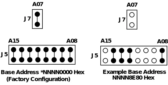
VMIVME-4132 32-Channel, 12-bit Analog Output Board with Built-In-TestBoard Address Selection (J5 and J7)
Jumpers J5 and J7 permit the VMIVME-4132 to be located on any 64-byte boundary within the short I/O address space. The short I/O address space consists of all the addresses between NNNN0000 HEX and NNNNFFFF HEX*. The VMIVME-4132 Board address is defined by nine lines, address bits A07 through A15. Six additional lines are used for programming the on-board registers (see Chapter 3 for more details).
[image:34.612.135.428.287.435.2]In programming the board’s base address, an installed jumper equals zero (0), and an omitted jumper equals one (1). Figure 2-2 shows an example base address as well as the factory-configured base address.
Figure 2-2 Base Address Selection
NOTE: The value NNNN depends on the make and model of the CPU board used.
Board Modifier Selection (J6)
The I/O access mode is programmed by selecting the responding state of the address modifier AM2 with jumper J6. Short supervisory access is the factory configuration and is selected by omitting the jumper. Short nonprivileged access is selected by installing the jumper. Figure 2-3 on page 35 shows the jumper location for the two different accesses.
A07 A07
J7 J7
J5 J5
A15 A08
A08 A15
Base Address *NNNN0000 Hex (Factory Configuration)
Base Address Configuration
2
Figure 2-3 Address Modifier Selection
Analog Output Voltage Range (J1 and J2)
The output voltage range is controlled by jumper J1. The factory configuration is the maximum full-scale range of 20 V. To change this value to 10 V, place a jumper in position 1-2. For a range of 5 V, place a jumper in position 2-3.
[image:35.612.233.421.394.547.2]Bipolar or unipolar operation of the analog outputs is selected with jumper J2. The board uses unipolar operations if a jumper is in position 1-2. If the jumper is in position 2-3, the outputs operate in bipolar mode which is the factory configuration. Figure 2-4 below shows the jumper locations for the different configurations.
Figure 2-4 Analog Output Voltage Range Selection J6
J6
Short Supervisory (Factory Configuration)
Short Nonprivileged
20 V (Factory Default)
J1 J1 J1
J2 J2
10 V 5 V
36
2
VMIVME-4132 32-Channel, 12-bit Analog Output Board with Built-In-TestLoopback Input Voltage Range (J3 and J4)
The loopback multiplexers drive an ADC (Analog-to-Digital Converter chip). The loopback voltage range and polarity must be the same as the output voltage range. If not, the ADC produces the wrong values. These conditions are controlled by jumpers J3 and J4. As with the outputs, the maximum full-scale range is 20 V. To modify the full-scale range for 5 V or 10 V, place the jumper at J4 in position 2-3. For 20 V operations, put the jumper in position 1-2.
[image:36.612.202.371.288.446.2]Bipolar or unipolar operation is selected with jumper J3. When J3’s jumper is in position 1-2, the board operates in the bipolar mode. For unipolar voltages, place the jumper in position 2-3.
Figure 2-5 Loopback Input Voltage Range Selection
Do not take readings of any output channel that was updated less than 3.4 msec before or you will read the old value of the outputs. The sequencer needs this time to refresh the output S&H buffer. Also, give the loopback multiplexer 5 msec after a start convert command before reading the ADC to give the multiplexer time to settle.
J3 J3
J4 J4
10 V or 5 V 20 V
Unipolar Mode Bipolar Mode
(Factory Default)
Calibration
2
Calibration
Before delivery from the factory, the VMIVME-4132 Board is fully calibrated and conforms to all specifications listed for bipolar operations. Should recalibration be required, perform the procedures in Analog Output Calibration Procedure on page 39 and Loopback Input Calibration Procedure on page 40 with the equipment listed in
Equipment Required below. The locations of all adjustments and test points are shown
in Figure 2-6 on page 38.
As delivered from the factory, all calibration adjustments are sealed against accidental movement. However, the seals are easily broken for recalibration. All adjustments should be resealed with a suitable fast-curing sealing compound after recalibration has been completed.
NOTE: Do not install or remove this board with power applied to the system.
Equipment Required
1. Digital Voltmeter (DVM): A meter with ±1.0000 VDC and ±10.000 VDC ranges, 5 or more digits, accuracy of ±0.005 percent, and 10 MW minimum input impedance.
2. Chassis: A VMEbus backplane or equivalent with J1 and J2 connectors, a VMEbus master controller, a +5 VDC ±0.25 VDC power supply, and one slot allocated for testing the VMIVME-4132 Board.
3. Extender Board: One VMEbus extender board.
38
[image:38.612.114.489.127.653.2]2
VMIVME-4132 32-Channel, 12-bit Analog Output Board with Built-In-TestFigure 2-6 Calibration and Test Points
J4
J3
R15
R14
R13
U2
R3
R2
R1
U1
TP2
TP1 TP3
U20
U19
J2 3 2 1
1 2 3
1 2 3
1 2 3 J1
Calibration
2
Analog Output Calibration Procedure
1. Install the VMIVME-4132 board on the extender board in the VMEbus backplane.
2. Remove any jumper from J1. (This sets the outputs to 20 V full scale.) 3. Place the jumper at J2 to the 2-3 position. (This is the bipolar setting.) 4. Apply power to the backplane and allow a minimum ten minute
warm-up time before proceeding.
5. Connect the digital voltmeter’s positive (+) lead to TP2 and its negative (-) lead to TP1.
6. Write the 16-bit value 0000 HEX to all of the analog output channels. These registers begin at offset address 40 HEX and stop at offset 7E HEX.
7. Adjust R1 for a digital voltmeter indication of 0.0000 ±0.0010 VDC.
8. Write the 16-bit value 07FF HEX to all of the analog output channels. These registers begin at offset address 40 HEX and stop at offset 7E HEX.
9. Adjust R2 for a digital voltmeter indication of +9.9951 ±0.0010 VDC.
NOTE: If the board is to be used in the Unipolar mode, perform steps 10, 11 and 12.
10. Move the J2 jumper to the 2-1 position, and place a jumper on J1 in the 1-2 position.
11. Write the 16-bit value 0800 HEX to all of the analog output channels. 12. Adjust R3 for a digital voltmeter indication of 0.0000 ±0.0010 VDC.
40
2
VMIVME-4132 32-Channel, 12-bit Analog Output Board with Built-In-TestLoopback Input Calibration Procedure
1. Perform the Analog Output Calibration Procedure before performing the Loopback Input Calibration.
2. Place the jumper at J4 in the 1-2 position. (This is the 20 V range.) 3. Place the jumper at J3 in the 1-2 position. (This is the bipolar setting.) 4. Write the 16-bit value 0000 HEX to all of the analog output channels. These
registers begin at offset address 40 HEX and stop at offset 7E HEX. 5. Write the 16-bit value 7840 HEX to the CSR at offset address 02 HEX. 6. While reading the ADC (a 16-bit word at offset address 04 HEX), adjust R15
(BIPOLAR OFFSET) for a reading of 0000 ±0001 HEX.
7. Write the 16-bit value 0FFF HEX to all of the analog output channels. These registers begin at offset address 40 HEX and stop at offset 7E HEX.
8. While reading the ADC (a 16-bit word at offset address 04 HEX), adjust R14 (GAIN ADJ) for an ADC indication that alternates between 0FFE and 0FFF HEX. 9. Repeat steps 4 through 8 until no further adjustments are required.
NOTE: If the board is to be used in the Unipolar mode perform steps 10, 11, 12 and 13.
10. Move jumper J3 to the 2-3 position. (UNIPOLAR OPERATION.)
11. Write the 16-bit value 0000 HEX to all of the output channels. These registers begin at offset 40 HEX and end at offset 7E HEX.
12. Write the 16-bit value 7840 HEX to the CSR at offset address 02 HEX.
13. While reading the ADC, adjust R13 (UNIPOLAR ZERO ADJUST) for an ADC indication of 0000 ±1 HEX.
14. For optimum performance, the gain may be adjusted. To make this adjustment, perform steps 8 and 9 above. Calibration of the loopback inputs is complete. Restore the board to its original configuration.
Connector Descriptions
2
Connector Descriptions
[image:41.612.208.438.290.706.2]Two 96-pin DIN connectors, P1 and P2 (Figure 2-7 on page 42), provide the VMEbus connections to the VMIVME-4132 Board. P1 contains the address, data and control lines, and all additional signals necessary to control the VMEbus functions related to the board. P2 provides some additional power connections for the board. A 64-pin DIN connector (P3) is used to connect the analog outputs to the user’s system. The orientation of the P3 connector is shown in Figure 2-6 on page 38, and the signal assignments are listed in Table 2-2. A twisted-pair ribbon cable with an overall shield is recommended for applications involving low-level signals in environments with a high degree of electrical noise.
Table 2-2 P3 Pin Channel Assignments
Pin No. Row A
Assignment
Row C Assignment
1 CH00 GND
2 CH01 GND
3 CH02 GND
4 CH03 GND
5 CH04 GND
6 CH05 GND
7 CH06 GND
8 CH07 GND
9 CH08 GND
10 CH09 GND
11 CH10 GND
12 CH11 GND
13 CH12 GND
14 CH13 GND
15 CH14 GND
16 CH15 GND
17 CH16 GND
18 CH17 GND
19 CH18 GND
20 CH19 GND
21 CH20 GND
22 CH21 GND
42
[image:42.612.227.347.155.565.2]2
VMIVME-4132 32-Channel, 12-bit Analog Output Board with Built-In-TestFigure 2-7 P3 Connector Pinout
A C
32 31 30 29 28 27 26 25 24 23 22 21 20 19 18 17 16 15 14 13 12 11 10 9 8 7 6 5 4 3 2 1
PC Board
CHAPTER
Programming
Contents
Control and Status Register Descriptions. . . 44
Initialization . . . 45
Controlling the Analog Outputs . . . 47
Testing The Analog Outputs Channels (BIT). . . 48
Program Example . . . 51
Introduction
Communication with the VMIVME-4132 Analog Output (AO) Board takes place through 64 contiguous 16-bit register locations mapped into the VMEbus short I/O address space. The short I/O address space consists of all locations within the address range from NNNN0000 HEX to NNNNFFFF HEX*. The functions of the board’s registers are summarized in Table 3-1 on page 45. These functions will be discussed in more detail later in this section.
The base address of the board holds the Board Identification Register. It is a read-only register that has a fixed value (17xx HEX). This register can be used by system initialization or automatic system configuration software. All of the other registers on the board are offset from the address assigned to this register.
44
3
VMIVME-4132 32-Channel, 12-bit Analog Output Board with Built-In-TestControl and Status Register Descriptions
The Control and Status Register (CSR) is located at offset address 02 HEX. It contains all of the flags necessary to control and monitor the following board operations:
• Analog outputs on-line/off-line status • Analog outputs refresh rate
• Digital-to-Analog (D/A) conversion • Built-in-Test (BIT) and A/D control
• Analog input channel selection (Built-in-Test only) • Front panel LED
• A/D and D/A enable/disable (Scan HALT)
Initialization
3
Initialization
When SYSTEM RESET is applied to the board, the Control Register and all converter flags are cleared to the LOW state ("zero"). This places the board in a known state. The D/A output sequencer is stopped and the A/D converter is disabled. The data format is offset binary, standard settling time, the LED is ON, and the outputs are
disconnected from the external circuits. In this condition the board is ready to perform loopback tests. After the system RESET is removed, the D/A sequencer starts and the A/D converter is enabled. The A/D and the D/A can be disabled under software control. Setting the SCAN HALT bit to a "one" disables the A/D and the D/A. This bit must be cleared before normal operation can begin.
[image:45.612.163.504.292.717.2]NOTE: *The value of NNNN depends on the make and model of the controlling CPU.
Table 3-1 VMIVME-4132 Register Map
Offset Address in HEX Register Name Access Mode 00 Board ID read (17xx Hex)
02 CSR read/write
04 ADC read
46
3
VMIVME-4132 32-Channel, 12-bit Analog Output Board with Built-In-TestControl and Status Register (CSR)
Control and Status Register Bit Definitions
Bit 15: D15 - Short Settling or New Data Rdy: Writing a "one" here reduces the time assigned for loopback settling from 5 to 3 msec. Reading a "one" here
indicates that loopback data is ready for the host to read.
Bit 14: D14 - LED Control: This bit turns the LED ON with a logic "zero" and OFF with a logic "one".
Bit 13: D13 - Start a Conversion or Converter Busy: Writing a "one" here and at D06 begins a loopback conversion. Reading a "zero" tells the host that a
conversion is done.
Bit 12: D12 - Two’s Complement Control: When a "one" is written here, the data is in offset binary form. When a "zero" is written here, the data is in two’s
complement form.
Bit 11: D11 - Outputs On-Line Control: When this bit is a "one", the output buffers are driving the cable and loopback buffers monitor the P3 pins. When it is a "zero", the outputs are disconnected from the cable and the loopback buffers monitor the output amps.
Bits 10, 09 and 07: D10, D09 and D07 - Reserved, Not Used
Bit 08: D08 - Fast Refresh: This speeds up the DAC control logic when a "one" is written here. Thus, the outputs get updated faster.
Bit 06: D06 - Start Settling or Settling Busy: Writing a "one" here and at D13 begins a loopback conversion. Reading a "zero" tells the host that the signal settling time is done.
Bit 05: D05 - Scan Halt: Writing a "one" here will stop the output sequencer and disable the A/D converter. This bit must be cleared before normal operations can begin.
Bit 04: D04 - MUX A4*: Loopback (input channel select) multiplexer control line.
NOTE: *The MUX signals are address lines. A decoder takes the state of these lines and selects the loopback buffer to convert.
Bit 03: D03 - MUX A3: Loopback (input channel select) multiplexer control line.
Bit 02: D02 - MUX A2: Loopback (input channel select) multiplexer control line.
Bit 01: D01 - MUX A1: Loopback (input channel select) multiplexer control line.
[image:46.612.62.522.126.208.2]Bit 00 D00 - MUX A0: Loopback (input channel select) multiplexer control line. Table 3-2 Control and Status Register (CSR) Bit Map
MSB Control and Status Register LSB
Bit 15 Bit 14 Bit 13 Bit 12 Bit 11 Bit 10 Bit 09 Bit 08
D15 D14 D13 D12 D11 D10 D09 D08
Bit 07 Bit 06 Bit 05 Bit 04 Bit 03 Bit 02 Bit 01 Bit 00
Controlling the Analog Outputs
3
Controlling the Analog Outputs
The 16 analog output channels appear to the controlling processor as 16 consecutive 16-bit words in the address space assigned to the VMIVME-4132 Board. The register map shown in Table 3-1 on page 45 lists the board-relative (or offset) address of each output channel. Each Analog Output Register supports both read and write
operations, eliminating the need for corresponding "shadow" latches in the processor Random Access Memory (RAM) space.
Writing to the Outputs
Output voltage data is recognized in the Analog Output Registers as right-justified 12-bit binary data. When offset binary data is written to a register, the upper four bits, D12 to D15, are ignored and not retained for read back. If the board is using two’s complement data, then these bits contain the sign of the output data. Each output responds to a new code within 3.4 msec after the code is written to the Output Register (0.85 msec in the Fast Refresh Mode). Be sure to give the board ample time to update the output before reading its value in a loopback test.
“Fast Refresh”
48
3
VMIVME-4132 32-Channel, 12-bit Analog Output Board with Built-In-TestTesting The Analog Outputs Channels (BIT)
Built-in-Test (BIT) provisions provide loopback testing of the outputs. These
capabilities permit self-contained, board-level verification of performance. The testing is controlled by seven bits in the CSR. They are the MUX Address lines, the start conversion, and start settling bits. The ON-LINE signal controls the source of the test voltage. The two’s complement bit dictates the format of the data. BIT is available at any time. The user picks a channel to monitor and orders a conversion. After 5 msec, the ADC is read and the read data is compared to the written data to determine the "health" of the channel. If an error is detected, the front panel LED can be used to locate the board in a system for troubleshooting.
Loopback Testing of the Outputs
The five least significant bits in the CSR, D00 through D04, and bit D11 are used to select the source of the voltage used in the loopback (BIT) test. D00 through D04 are the loopback multiplexer select lines MUX A0 through MUX A4. They select the input to be tested. Bit D11, the outputs on-line control, selects where the input sample will be made. When this bit is low the loopback test buffers monitor the analog output buffers. If this bit is high, the test buffers monitor the output pins of P3. The loopback multiplexers are always enabled to prevent the ADC from trying to convert a high impedance input instead of a voltage. By routing the analog outputs through these loopback multiplexers, the operation of all the components on the VMIVME-4132 Board can be verified.
ADC Controls and Flags
All timing operations for the ADC are performed by an on-board controller. User control of the converter consists of the following control bits, flags, and registers. The control bits and flags in the CSR are summarized in the following paragraphs. They are restated here for clarity.
CSR Bit Functions
Control Bits
• SHORT SETTLING H . . .D15 * • EN START CONV H . . . .D13 * • TWO's COMPL L . . . D12 • START SETTLING H . . . D06 *
NOTE: * Effective only upon writing ("strobed").
Flags (Status Register)
• NEW DATA RDY H . . . . .D15 * • CONV BUSY H . . . .D13 • SETTLING BUSY H . . . .D06
Testing The Analog Outputs Channels (BIT)
3
The START SETTLING and START CONV controls are essentially strobes. They are effective only at the moment of writing to the Control Register. Although supplied as two separate control bits, they must be written to the register simultaneously along with the operating mode (TWO’s COMPL L and SHORT SETTLING H bits) and the input channel selection. Thus, a single write to the CSR can start a conversion. Once started, the user simply waits 5 msec and then reads the ADC. The NEW DATA RDY bit can be used as a pass or fail indicator. Polling this bit (or any other bit on the board) will degrade the loopback readings.
[image:49.612.121.533.365.494.2]For example, to convert the signal of Channel 0, with the outputs on-line using offset binary data format, write 7840 HEX to the CSR. The low 5 bits select the output channel to monitor (Channel 0 in this case). The upper 4 bits starts the conversion and selects the data format. Now wait 5 msec to give the multiplexers time to settle. In this time, the host can do whatever it wants. Then the ADC is read. The ADC is read via the Converter Data Register (CDR). To check Channel 12, write 784C HEX to the CSR. The CDR is a 16-bit read-only register at relative address 04 HEX. It is used to store the ADC data. Data in this register is 12 bits, right-justified. D12 through D15 are always "zero" in the binary data format, and are sign extensions in the two’s complement data format. The data format depends upon the state of the TWO’s COMP L control bit in the CSR. Converter output codes that are produced at major points within the full-scale ranges shown are summarized in Table 3-3 through Table 3-5 on page 50.
Table 3-3 Data Codes for Unipolar Output Voltages
Unipolar Range Straight Binary
Input +5 V
VFSR=5V
+10 V
VFSR=10V D15* D00 Hex
+FS-1 LSB +4.9988V +9.9976V 0000 1111 1111 1111 FFF 3/4 FS +3.7500V +7.5000V 0000 1100 0000 0000 C00 1/2 FS +2.5000V +5.0000V 0000 1000 0000 0000 800 1/4 FS +1.2500V +2.5000V 0000 0100 0000 0000 400 1 LSB +0.0012V +0.0024V 0000 0000 0000 0001 001 Zero 0.0000V 0.0000V 0000 0000 0000 0000 000
Table 3-4 Data Codes for Bipolar Output Voltages
Bipolar Range Offset Binary
Input +5 V
VFSR=10V
+10 V
VFSR=20V D15* D00 Hex
[image:49.612.120.530.526.719.2]50
3
VMIVME-4132 32-Channel, 12-bit Analog Output Board with Built-In-TestSTRAIGHT BINARY: VO =VFSR (D1 ÷ 4096), D1 = Dec. equiv. of HEX value OFFSET BINARY: VO =VFSR (D1 ÷ 4096) - (VFSR ÷ 2). D2 = Dec. equiv. of HEX value 2’s COMPLEMENT: VO =VFSR (D2 ÷ 4096) - (VFSR ÷ 2). D2 = Dec. equiv. of (HEX value ⊕ $800)
* = Zero (binary) or extended sign (2’s comp); ⊕ = Exclusive OR’d with.
For any offset binary converter output code (BIPOLAR RANGE), the associated output voltage is obtained with the expressions:
OUTPUT (Volts) = (-EFSR/2 )+ (EFSRX [OUTPUT DATA IN DECIMAL] /4096).
The output voltage for a straight binary code (UNIPOLAR RANGE) is: OUTPUT (Volts) = +EFSR X [OUTPUT DATA IN DECIMAL] / 4096.
Where EFSR is the full-scale range voltage. (E.g.: EFSR = 10 V for the ±5 V range.)
For example, the output voltage for a HEX value of 51A is found like this: • Convert 51A (HEX) to its decimal equivalent, which is 1306.
• Identify the Range you are using, for example ±5 V. This range uses the bipolar equation with EFSR= 10 V.
[image:50.612.84.494.102.297.2]• Compute the result by substituting these numbers in the equation. OUTPUT (Volts) = -(10/2) + (10 x (1306/4096)) = -5 + (10 x .32) = -1.81 V.
Table 3-5 Data Codes for Bipolar 2’s Complement Output Voltages
Bipolar Range 2’s Complement
Input +5 V
VFSR=10V
+10 V
VFSR=20V D15* D00 Hex
Program Example
3
Program Example
The following is a sample program to perform some simple board operations. The program is written in C.
/*
** VMIVME 4132 sample code header file
*/
typedef unsigned short word; /* data type of word */
#define VME_SHORT_IO 0xfbff0000 /* Force Cpu short io */
#define vmic4132_base_address 0x0000 /* Jumper Field J5 & J7 */
struct vmivme4132 {
word bid; /* board ID register */
word csr; /* control status register */
word adc; /* ADC converter data register */
word reserved[29]; /* unused - reserved */
word dac[32]; /* DAC channels 0 - 31 */
};
typedef struct vmivme4132 vmic4132_reg;
#define SHORT_SETTLING 0x8000 /* CSR control bits (write) */
#define LED_OFF 0x4000
#define START_CONVERT 0x2000
#define TWOS_COMPLEMENT0x1000 0x1000 #define OUTPUTS_ONLINE 0x0800
#define FAST_REFRESH 0x0100
#define START_SETTLING 0x0040
#define SCAN_HALT 0x0020
#define NEW_DATA_READY 0x8000 /* CSR status bits (read) */ #define CONVERTER_BUSY 0x2000
#define SETTLING_BUSY 0x0040
/* VMIVME 4132 sample code */
#include"x4132.h"
52
3
VMIVME-4132 32-Channel, 12-bit Analog Output Board with Built-In-Testword board_id,status,adc_cword,data_in; /* init pointer to 4132 board */
vmic4132_reg * vmic4132;
vmic4132 = (vmic4132_reg *)(VME_SHORT_IO+vmic4132_base_address);
vmic4132->csr = LED_OFF | OUTPUTS_ONLINE;/* init dac outputs */ board_id = read_id(vmic4132); /* read board id register */
status = read_csr(vmic4132); /* read control/status register */
write_dac(0,0x100,vmic4132); /* write dac channel 0 with 100 hex */
/* init adc control word and read back dac output with adc converter */
adc_cword = LED_OFF | START_CONVERT | OUTPUTS_ONLINE | START_SETTLING; data_in = read_adc(0,adc_cword,vmic4132);
data_in = read_adc(0,adc_cword,vmic4132);
} /* end main */
/*
** 4132 function primitives */
word read_id(vmic4132_reg * board) {
return board->bid; }
word read_csr(vmic4132_reg * board) {
return board->csr; }
void write_dac(word chan,word data,vmic4132_reg * board) {
board->dac[chan] = data;
}
word read_adc(word chan,word ctrl,vmic4132_reg * board)
{
board->csr = (ctrl+chan);
while (!(board->csr & NEW_DATA_READY));/* test new data ready bit */
return board->adc;
Maintenance
Maintenance
This section provides information relative to the care and maintenance of VMIC’s products. If the product malfunctions, verify the following:
• System power • Software
• System configuration • Electrical connections
• Jumper or configuration options
• Boards are fully inserted into their proper connector location • Connector pins are clean and free from contamination
• No components of adjacent boards are disturbed when inserting or removing the board from the chassis
• Quality of cables and I/O connections
If products must be returned, contact VMIC for a Return Material Authorization (RMA) Number. This RMA Number must be obtained prior to any return.
VMIVME-4132 32-Channel, 12-bit Analog Output Board with Built-In-Test
54