PREFACE
This manual describes the organization and functional characteristics of the Amdahl 4 70V /6, a very high-speed, large scale general purpose computing system. It provides machine reference data of fundamental interest and value to management, systems analysts, programmers and operations personnel.
Details' on machine organization, performance and configuration are provided. Supplementary data on characteristics of machine check conditions, instruc-tion timing formulas, specific channel characteristics and console operation is provided as appendices.
SECOND EDITION:
Amdahl Corporation Machine Reference Manual, Form MRM 1000-I.
This manual has been prepared by Amdahl Corpora-tion Technical PublicaCorpora-tions.
INTRODUCTION
The Amdahl 470V/6 computing system provides ex-tremely powerful, high-5peed, general-purpose com-puting capabilities for sophisticated business and scientific applications. The high performance of the Amdahl 470V/6 results primarily from a newly-designed high-5peed circuitry with internal speeds measured in picoseconds, packing densities with up to 100 circuits on a central processor chip, a sophisticated architecture that incorporates the pipe-line concept for a high concurrency of operations, ef-ficient algorithms for high-5peed internal functions, and a high-5peed buffer coupled with monolithic main store for fast data access times. A highly-flexible input/output channel scheme is also provided for the Amdahl 470V/6. Sixteen inboard 110 chan-nels are standard and may be configured in any com-bination of byte or block multiplexer or selector channels. These inboard channels operate inde-pendently from the central processor.
The central processor and most of the channel unit are implemented with high-5peed large scale integra-tion (LSI) circuitry, which enables a six-to-eight times reduction in overall size and the number of external connections. The reduction in size and com-plexity becomes immediately obvious in that the central processor and the LSI portion of the channels occupy only 51 cards. Each card, or multichip carrier (MCC), is a ten-layer printed circuit board with 42 chip positions in a 7W' square area.
TABLE OF CONTENTS
INTRODUCTION .•.•••••••••.••••••••••••.•..•••.••..••••.• ii
SYSTEM OVERVIEW • • . . • • . • • . . • • • • . • • . • • . . • . • • . . . . • . . . • . . • • 3
Central Processor . . . • . . • . . . 5
Main Storage . . . • . . . 5
Channels . . . 5
System Console. . . • . . . .5
Power Distribution Unit . . . 5
Optional Features . . . • . 5
CPU-MAIN STORAGE SYSTEM • . • . . . • • • . . • . • . . . . • . . . • . • • . . . . 6
Instruction Unit . . . 7
Execution Unit. . . .. 8
Storage Control Unit. . . • . . . .. 10
High-Speed Buffer. . . .. 10
Buffer Operation. . . • . . . .. 10
Virtual Address Operation. . . .. 11
TLB Operation. . . .. 12
STO Stack Operation. . . .. 13
CHANNEL FACILITIES • . • . . • • . . . . • • • • • • . • • • • • • • • • • . . • . • • .. 14
Central LSI Channel. . . .. 15
Modes of Channel Operation. . . .. 17
SYSTEM CONSOLE ....••..•..•.••••..••.•••••.•.••••••.•. 19
Usage Metering. . . .. 20
Operator's Console Programming . . • . . . .. 21
APPENDIX A: MODEL·DEPENDENT FUNCTIONS • . . . • . • • . . • . . . . • . . 23
Instruction Set Differences . . . 24
CPU Logout Areas . . . • . . . • 24
Fixed Logout Area . . . 24
Extended CPU Logout . . • . . . 26
Machine Checks . . . • . . . • 26
Machine Check Conditions . . . 26
Machine Check Interrupts . . . 27
Hardware Diagnostic Mode . . . • . . . 28
APPENDIX B: INSTRUCTION TIMING ESTIMATES .•..•..••••..••.• 29
Early Condition Code Settings . . . 30
Retryable Instructions . . . • • . . . 30
Timing Formulas . . . 31
Legend for Timing Formulas . . . 35
Special Timing Formulas . . . 37
APPENDIX C: MODEL-DEPENDENT CHANNEL FUNCTIONS •.•...••.• 41
Subchannel Assignment . . . • . . . 42
Extended Channel Logout . . . 44
APPENDIX D: CONSOLE PROCESSOR SYSTEM . . . . • . . • . . . . '" .•.. 49
Modes of Operation . . . 50
Amdahl 470V/6 Power Up and Power Down . . . . , . . . 50
Initialization . . . • . . . 51
Initial Program Load . . . " . . . 51
Status Display . . . 52
Errors . . . 54
Control Mode Operation. . . . . . 55
Control Mode and Device Support Mode Commands . . . 56
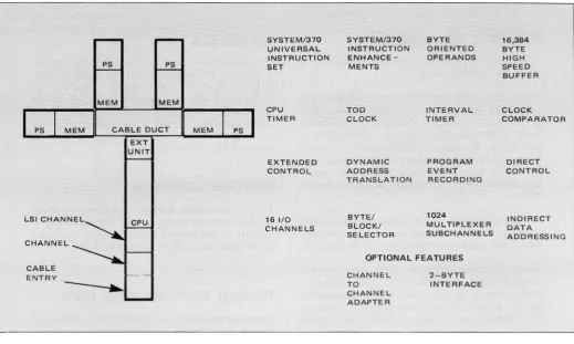
SYSTEM OVERVIEW
MEM
LSI CHANNEL CHANNEL
CABLE ENTRY
PS PS
MEM MEM
CABLE DUCT EXT UNIT
MEM
SYSTEM/370 UNIVERSAL INSTRUCTION SET CPU TIMER EXTENDED CONTROL
16 I/O CHANNELS
> SYSTEM/370
INSTRUCTION ENHANCE -MENTS TOD CLOCK DYNAMIC ADDRESS TRANSLATION BYTE/ BLOCK/ SELECTOR BYTE ORIENTED OPERANDS INTERVAL TIMER PROGRAM EVENT RECORDING 1024 MULTIPLEXER SUBCHANNELS OPTIONAL FEATURES
CHANNEL TO CHANNEL ADAPTER
2-BYTE INTERFACE 16,384 BYTE HIGH SPEED BUFFER CLOCK COMPARATOR DIRECT CONTROL INDIRECT DATA ADDRESSING
OPERATOR'S CONSOLE 3066 EMULATION 3215 EMULATION SYSTEM CONSOLE WITH CRT DISPLAY
[image:7.613.56.575.47.357.2]CENTRAL PROCESSOR
The Amdahl 470V/6 central processor includes the following standard features:
STANDARD ARCHITECTURE. TheAmdahl470V/6 follows the architecture of System/370 as specified in the IBM Systeml370 Principles of Operation, GA22-7000 (henceforth referred to as Principles of Operation). The standard full System/370 Universal Instruction Set with extended precision floating point operations, direct control and System/370 instruc-tion enhancements are implemented on the Amdahl 470V/6.
DIRECT CONTROL. . This facility provides a direct control path into the central processor from external . devices and operates independently of the channels. 16K-BYTE HIGH-SPEED BUFFER. The standard buffer size provides 16,384 bytes of high-speed bi-polar memory to maximize system throughput. Memory transfer width to the buffer is 32 bytes and CPU transfer width from the buffer is 4 bytes. TRANSLATION LOOKASIDE BUFFER. To en-hance virtual performance the Amdahl 470V/6 pro-vides a 256-entry translation lookaside buffer (TLB). This TLB provides high-speed storage of most re-cently used virtual address translation information. Operation of the TLB is further enhanced with a 32-entry segment table origin stack to identify specific CPU states with TLB entries.
TIMING FACILITIES. Standard timing facilities of System/370 architecture are provided. These include an interval timer, time-of-day (TOD) clock (a 64-bit field with 52-bit resolution), a clock comparator (provides a 52-bit comparison field for the TOD clock) and CPU timer.
MAIN STORAGE
Main storage is available in one megabyte increments, up to eight megabytes. Interleaving is four-way for each two megabyte storage unit and two-way if one megabyte is installed in a storage unit. Thus, a three megabyte system is four-way interleaved for the first two megabytes and two-way interleaved for the last odd megabyte.
CHANNELS
The Amdahl 470V/6 system has 16 inboard channels, which may be installed in any· combination of se-lector, or byte or block multiplexer channels. The operation of these channels does not interfere with the operation of the CPU, except for possible storage access conflicts. A total of 1024 sub channels may be assigned to the multiplexer-type channels in groups of 64, 128, or 256.
SYSTEM CONSOLE
The system console performs operations and main-tenance functions for the Amdahl 470V/6 system. It
includes an independent console processor, operator control panel and CRT display and keyboard.
POWER DISTRIBUTION UNIT.
The power distribution unit (PDU) distributes 400 Hz and 60 Hz power to the Amdahl 470 V/6 system. Emergency power off and thermal monitoring fa-cilities are also provided.
OPTIONAL FEATURES
CHANNEL-TO-CHANNEL ADAPTER. This option provides the necessary synchronization to intercon-nect two channels. It may be attached to either a selector or block multiplexer channel and uses one control unit position on each channel. Only one of the channels need have the feature installed, however. When interconnecting an Amdahl 470V/6 system with an IBM System/360 or /370, either may be equipped with the channel-to-channel adapter.
CPU-MAIN STORAGE SYSTEM
INSTRUCTION UNIT
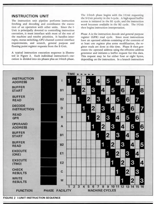
The instruction unit pipeline performs instruction fetching and decoding and coordinates the execu -tion of an operation with other units. Since the 1-Unit is principally devoted to controlling instruction execution, it must interface with most of the rest of the machine and resolve priorities. It handles inter-rupts; status switching; CPU-channel control interface requirements; and scratch, general purpose and floating point register requests from the E-Unit.
A typical instruction execution sequence is ill ustra-ted in Figure 2. Each individual instruction's exe -cution is divided into six phases plus an I-fetch phase.
INSTRUCTION
ADDRESS
BUFFER
START
B1
BUFFER
READ
B2
DECODE
INSTRUCTION
D
READ
GPR
R
OPERAND
A
ADDRESS
BUFFER
START
B1
BUFFER
B2
READ
EXECUTE
(ONE)
E1
EXECUTE
(TWO)
E2
CHECK
C
RESULTS
WRITE
W
RESULTS
The I-fetch phase begins with the I-Unit requesting the S-Unit priority in the I-cycle. A high-speed buffer access is initiated in the Bl cycle, and the instruction wonl becomes available in the B2 cycle. The I-Unit then begins instruction interpretation.
Phase A is the instruction decode and general purpose register (GPR) read cycle. Since most instructions have an operand address consisting of the contents of at least one register plus some modification, the re-gister reads are done at this time. Phase B then gen-erates the operand address using the effective address generator and initiates a buffer request for this data.
This request may be for either four or eight bytes, depending on the instruction. In a branch instruction
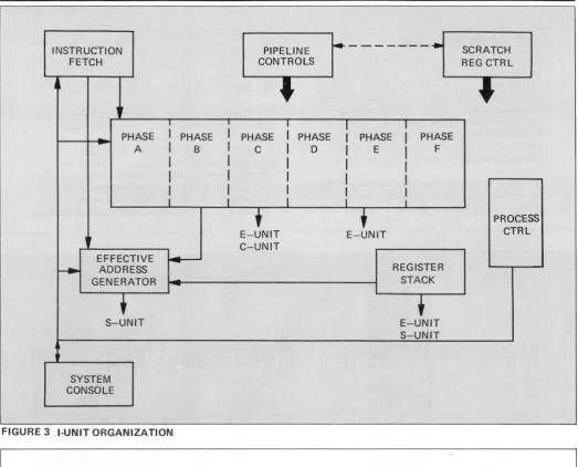
[image:10.613.42.578.28.738.2]INSTRUCTION FETCH
PIPELINE
f4---.
SCRATCHCONTROLS REG CTRL
I
+
PHASEA
EFFECTIVE ___ ADDRESS
GENERATOR
+
S-UNITSYSTEM CONSOLE
I
I
I
I
I
I
IFIGURE 3 I-UNIT ORGANIZATION
PHASE
I
PHASEB
I
CI
I
I
IE-~NIT
C-UNIT-the target of the branch is requested so that both paths of the branch will be available. (The branch-not-taken path continues to be fetched and decoded). After data has become available from the S-Unit in Phase C, the I-Unit passes this data to the E-Unit to begin execution. The E-Unit sets early condition codes at the end of the El cycle, thus informing the I-Unit of the proper path for branches before
in-I
I
I
I
I
I
I
f
I
IPHASE
I
PHASEI
PHASED
I
EI
FI
I
I
I
I
I
I
+
PROCESSE-UNIT CTRL
REGISTER STACK
+
E-UNIT S-UNITAnother feature of the delayed wntmg of results appears in I-Unit interrupt handling. Since the pipe-line can be "backed up" an interrupt need wait oilly for completion of the current instruction (on noninterruptable instructions) before the in-terrupt can be taken; hence, all interrupts on the Amdahl 4 'lOV /6 are precise.
[image:11.613.31.554.45.467.2]results on single cycle boundaries thereafter.
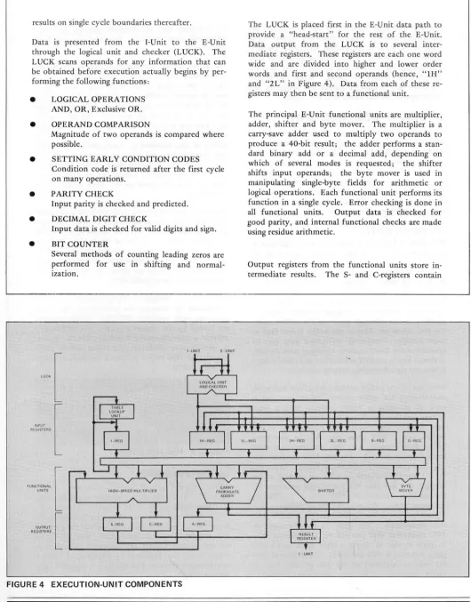
Data is presented from the I-Unit to the E-Unit through the logical unit and checker (LUCK). The LUCK scans operands for any information that can
be obtained before execution actually begins by
per-forming the following functions:
• LOGICAL OPERATIONS AND, OR, Exclusive OR.
•
•
•
•
OPERAND COMPARISON
Magnitude of two operands is compared where possible.
SETTING EARLY CONDITION CODES Condition code is returned after the first cycle
on many operations.
PARITY CHECK
Input parity is checked and predicted.
DECIMAL DIGIT CHECK
Input data is checked for valid digits and sign.
• BIT COUNTER
Several methods of counting leading zeros are
performed for use in shifting and normal-ization.
I_UNIT S c..t)N1T
'
"
{
REINPUT GISTERS [
FUNCTIONAL
r-UNITSL
OUTPUT [
REGISTERS
The LUCK is placed first in the E-Unit data path to provide a "head-start" for the rest of the E-Unit. Data output from the LUCK is to several inter-mediate registers. These registers are each one word wide and are divided into higher and lower order words and first and second operands (hence, "lH"
and "2 L" in Figure 4). Data from each of these
re-gisters may then be sent to a functional unit.
The principal E-Unit functional units are multiplier,
adder, shifter and byte mover. The multiplier is a carry-save adder used to multiply two operands to
produce a 40-bit result; . the adder performs a stan-dard binary add or a decimal add, depending on which of several modes is requested; the shifter shifts input operands; the byte mover is used in
manipulating single-byte fields for arithmetic or
logical operations. Each functional unit performs its function in a single cycle. Error checking is done in all functional units. Output data is checked for good parity, and internal functional checks are made using residue arithmetic.
[image:12.612.46.576.52.729.2]the sum and carry outputs of the multiplier; the A-register contains output from the adder. The I -register is used in generation of 10-bit inverses, which are created by the table-lookup unit, or divi-sion operations. The B- and G-registers are used for intermediate storage of fields. When the E-Unit functions are complete, results are staged in the result register for transmission to the I-Unit.
STORAGE CONT
ROL UNIT
All storage requests from the CPU and channels are processed by the storage control unit. Priorities are resolved and facilities are provided based on the S-Unit's internal priority structure and the priority of the request from the 1- or C-Unit. The S-Unit also determines whether requested data comes di-rectly from the high-speed buffer or must be read in from main storage. All virtual-to-real address trans-lations are performed by the S-Unit.
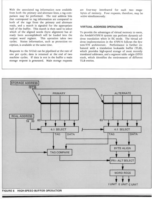
HIGH-SPEED BUFFER
The 4 70V /6 high-speed buffer (HSB) is organized as a 16,3 84-byte set-associative memory consisting of primary and alternate halves. Each half contains 256 32-byte lines that can be accessed on a double or single word basis. Because of the local nature of most programs, execution time should be related to buffer speed rather than main storage speed. This significant improvement in speed is further enhanced by the non-store-through nature of the buffer; mean-ing that stores are done to the buffer rather than to main storage. Frequently referenced data may be accessed many times without updating main storage.
A stored line is marked as modified and main storage is updated asynchronously only as necessary.
Each line of the buffer contains a tag field that holds modification and other control information and is used to associate a buffer location with a main storage location (see Figure 5). The block identifier field contains higher-order real address bits of the buffer data. With these bits and the associated buffer data location, a unique mapping to a main storage line is defined. The key field contains five
bit, indicates that the primary location has been referenced more recently than the associated al-ternate location.
The above factors are variables used by the S-Unit to determine where to put new data in the buffer. If
data is not present in the buffer when requested, it may be moved to either the primary or alternate half of the buffer from main storage. The S-Unit can check to see if either the associated primary or alter-nate location is invalid (and thus may be loaded im-mediately) or which was used more recently. A facility is also provided to distinguish between CPU and channel data and between supervisor and pro-blem state. The ability to change buffer algorithms further enhances buffer tuning and provides for the most efficient operation under a wide variety of cir-cumstances.
The S-Unit may also use a prefetch function to fetch data from main storage in advance of need. This pre-fetch may occur after either the first or second access to any quarter-line segment of the buffer. Prefetch may be selectively enabled for the channel, instruc-tion fetch or operand fetch port. Prefetch and buf-fer change algorithms are preset by Amdahl to op-timal values for most applications.
All the above changes to S-Unit algorithms are ac-complished by changing the contents of the S-Unit operating state registers (OPSRs). These registers are loaded by the system console. The OPSRs also provide a reconfiguration capability for the buffer. In case of error conditions, the buffer may be parti-tioned such that only a portion is enabled, disabling the part in error.
BLOCK IDENTIFIER KEY REF CNTRL I I
:1:1
nl
I
(Real Address Bits) 0 ••• 4 P C R1 R2 012 I I
I
With the associated tag information now available from both the primary and alternate lines, a tag com-parison may be performed. The real address bits that correspond to tag information are compared to both of the tags from the primary and alternate reads, and a match is signaled for the appropriate half of the buffer. This match is then used to select which of the aligned words (byte alignment has al-ready been accomplished) will be loaded into the output word register. This operation takes two cycles. Status information, such as protection ex-ception, is available at the same time.
Requests to the S-Unit can be pipelined at the rate of one per cycle; data is returned at the end of two machine cycles. If data is not in the buffer a main storage request is generated. Main storage requests
PRIMARY
REAL ADDRESS
are four-way interleaved for each two mega-bytes of memory. Four requests, therefore, may be active simultaneously.
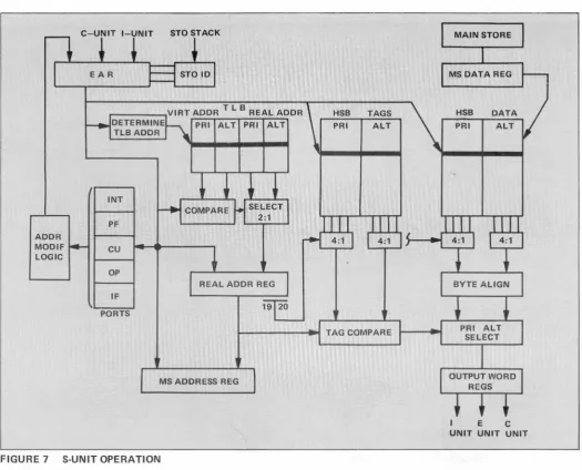
VIRTUAL ADDRESS OPERATION
To provide the advantages of virtual memory to users, the Amdahl 470V/6 system can perform dynamic dress translation when in EC mode. The virtual ad-dress implementation in the 4 70V 16 follows the
Sys-tem/370 architecture. Performance is further en-hanced with a translation lookaside buffer (TLB), which provides high-speed storage of most recently translated addresses, and a segment table origin (STO) stack, which identifies the environment of different TLB entries.
[image:14.612.47.577.46.740.2]TLB OPERATION
The TLB provides a fast source of translation inform-ation to minimize virtual operation time and to allow overlap of translations and HSB accesses. The TLB is implemented very similarly to the HSB, but consists of 128 virtual-real address pairs in each of the pri-mary and alternate halves. Thus, a correspondence is set up in the TLB between virtual and real address space whenever a translation is performed.
When a virtual address is presented to the S-Unit through the effective address register (EAR), a TLB and an HSB access are both started (see Figure 7). The virtual address maps to a given TLB location.
PRI ALT PRI ALT
INT
PF ADDR
MODIF CU LOGIC
OP
IF
When the associated real address is obtained from the TLB (assuming that an entry was there), a selection is performed based on matching the virtual address in the TLB with the virtual address presented. The real address register (RAR) is then loaded with the effective real line address, and bits 19-20 are used for buffer data selection as described above. If data is not present in the buffer, the real byte address is loaded in the main store address register (MSAR) to obtain data from main storage. S-Unit ports are provided for each of the possible requesting units (instruction fetch, operand, C-Unit, pre-fetch and internal ports) to allow the capability of having requests from the various units active simultaneously.
HSB TAGS
[image:15.613.30.555.299.723.2]If the virtual-real address translation has been per-formed and information resides in the TLB, no overhead for the TLB access occurs since its access is overlapped with the buffer; thus, data is returned in two cycles for both real and virtual operations. ~f the virtual-real address pair is not currently valid m the TLB a full translation must be made which requires two additional storage (either
b~ffer
or ~ain store) ref.erences. The new translation is placed m the TLB usmg an algorithm similar to the buffer replacement algorithm. A hotlcold (Hie) bit feature similar to the feature of the HSB is implemented in the TLB.TLB addresses may be made invalid by a system reset, a Purge TLB instruction, or by changing the state of control registers 0 and 1. To enhance performance, two sets of valid bits are kept in the TLB. When a Purge TLB instruction is executed, the S-Unit auto-m~tically switches the set of valid bits it is currently usmg to the other set, which are all marked "invalid". The S-Unit resets the older set of valid bits during spare cycles to be ready for the next Purge instruc-tion; thus a single Purge TLB instruction may be ~xecute?, incurring only the minimum two cycle mstructlOn overhead.
STOSTACK OPERATION
The STO stack stores information about control registers 0 and 1 so that TLB entries can be reused if these control registers are reloaded with previous values. This is done by associating a STO identifi-cation field (ID) with translation information from control registers 0 and 1. The STO ID is then stored with the TLB and STO stack entries. Valid TLB en-tries must match the current STO stack entry (which matches current values in control registers 0 and 1).
CHANNEL FACILITIES
The Amdahl 470V/6 has 16 standard inboard channels. These channels are independent of the CPU and, with the possible exception of memory access conflicts, do not affect CPU performance. The channels may be configured in any combination of selector channels or byte or block multiplexer chan-nels. A total of 1024 sub channels are available for allocation to multiplexer channels in groups of 64, 128 or 256.
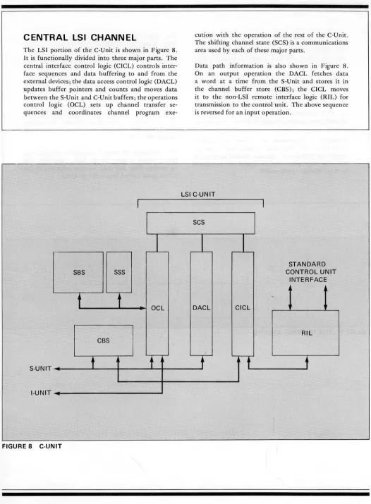
CENTRAL LSI
C
HANNEL
The LSI portion of the C-Unit is shown in Figure 8.
It is functionally divided into three major parts. The central interface control logic (CICL) controls i nter-face sequences and data buffering to and from the external devices; the data access control logic (DACL)
updates buffer pointers and counts and moves data between the S-Unit and C-Unit buffers; the operations control logic (OCL) sets up channel transfer se-quences and coordinates channel program exe
-ii
I
SBS SSS
t
OCl+
CBS
S-UNIT
t
t
I-UNIT
FIGURE 8 C-UNIT
cution with the operation of the rest of the C-Unit. The shifting channel state (SCS) is a communications
area used by each of these major parts.
Data path information is also shown in Figure 8.
On an output operation the DACL fetches data a word at a time from the S-Unit and stores it in the channel buffer store (CBS); the CICL moves it to the non-LSI remote interface logic (RIL) for transmission to the control unit. The above sequence is reversed for an input operation.
lSI C-UNIT
SCS
"
I
I
STANDARD CONTROL UNIT
INTERFACE
-,
DACl CICl
;
Ril
,
[image:18.612.52.578.34.749.2]The CICL transfers data to or from the CBS on even cycles; the DCL and DACL share odd cycles.
The CICL transfers one byte or two bytes at a
time; the DACL and DCL transfer a word at a time.
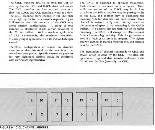
The CICL examines every channel in the SCS once
every eight cycles for data transfer requests. Figure
9 illustrates how this property of the CICL may
affect channel configuration. A group of four
channels as illustrated shares certain resources of
the C-Unit buffers. With a machine cycle time
of 32.5 nanoseconds, the maximum bandwidth
of each group is approximately 3.85 million bytes per
second.
Therefore, configuration of devices on channels
must insure that this total transfer rate is not
ex-ceeded for each group. Specific channel assignments
for very high-speed devices should be confirmed with an Amdahl representative.
9
10 11 12H, c' eo; 'i.
,
,eo [image:19.612.29.554.74.514.2]1
2
3
4
FIGURE 9 CICL CHANNEL GROUPS
The DACL is pipelined to optimIZe throughput.
Each channel is examined every 16 cycles. Thus, while one section of the DACL may be fetching
data from the S-Unit, another may be posting results
to the SCS, and another may be examining the
incoming SCS for channels that need service. Each
channel is assigned a dynamic priority based on
the amount of space it has remaining in the C-Unit
buffers. If a channel has less than half of its buffer
remaining, the DACL will change its S-Unit request from a low to a high priority. This change can occur even if a fetch or a store is in progress. The highest priority channel is marked from the SCS and serviced next by the DACL.
The translation of channel commands to CICL and
DACL action is done by the DCL. The DCL sets
up counts, flags and data transfer addresses in the C-Unit local buffers (normally the CBS).
13
14
150
.
To perform byte or block multiplexing, the OCL activates a sub channel (the portion of a channel that actually "executes" a channel program) when appropriate status information is received from the CICL. The OCL uses the subchannel buffer store (SBS) for temporary storage of inactive sub-channel information. The OCL can monitor sub-channel state and perform subsequent decisions with the information from the sub channel state store (SSS). The OCL obtains its control information directly from the I-Unit and S-Unit over an interface ·shared with the DACL.
Channel indirect data addressing as described in the Principles of Operation is fully implemented on the Amdahl 470V /6 by the OCL and DACL. Indirect data addressing (IDA) requires that a control pro-gram perform any necessary virtual-to-real address translations before a data transfer command is executed by the channel.
MODES OF CHANNEL
OPERATION
Because of the relative independence of the OCL, DACL and CICL, any channel can be configured as a byte or block multiplexer or selector. Selector channels transfer only in burst mode and may address up to 256 I/O devices, one at a time. Selector channels contain a single implicit subchannel, which does not require allocation from that pool of 1024 sub channels. The total possible data rate per selector channel is the same as the rate for a block multi-plexer.
Multiplexer-type channels perform device multi-plexing and execute several channel programs simul-taneously. The level of concurrency is determined by the number of subchannels allocated to the multiplexer channel; one subchannel is necessary for
each concurrent channel program execution. Sub-channels are allocated in groups of 64, 128 or 256. With either 64 or 128 assigned sub channels, a channel may be configured for shared subchannel operation. Details on shared subchannel allocation and device address assignment are contained in Appendix C.
Block multiplexer channels perform the basic multiplexer function, but always transfer in burst mode. It is the more efficient type of multiplexer channel since a considerable amount of data is trans-ferred each time a device logically connects to a channel. Maximum data rate on a standard single-byte block multiplexer channel is the same as for any channel operating in burst mode, or approxi-mately two million bytes per second. The optional two-byte bus doubles this available channel band-width.
Byte multiplexer channels usually multiplex a very few bytes at a time. The Amdahl 470V/6 allows a byte multiplex-mode bandwidth of approximately 110 kilobytes per second. The byte multiplexer bandwidth for single-byte bus devices running in burst mode is approximately two million bytes per second. Selector sub channels are not implemented in the Amdahl 4 70V /6 byte multiplexer channels.
Extended channel logout is fully implemented on the Amdahl 470V/6. If control register 14 bit 2 is set, extended logouts will be made when certain errors occur. No logout will be made if this bit is off. More information on extended channel logout fields is found in Appendix C.
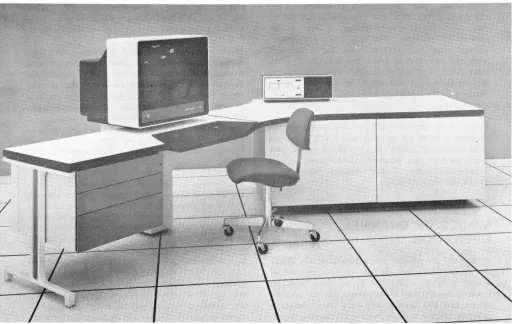
SYSTEM CONSOLE
The Amdahl 470V/6 system console serves as an operator's console and as a system maintenance con-sole (Figure 10). It consists of a CRT and keyboard, an independent console processor, a disk for the console processor, a diskette unit to provide the Amdahl field engineer with a diagnostic test loading facility, and a modem to allow remote access to the Amdahl diagnostic facility. A standard channel interface allows tpe console processor to emulate a 3066 or 3215 operator's console. A standard operator's control panel is also provided (Figure 11).
The Amdahl 470V/6 system console can operate in three modes. Device support mode provides emulation of standard consoles for data transmission to and from the operator using the system console and a channel; hardware command mode allows display and storage of registers and memory, reset, clear, and other hardware functions; and maintenance mode allows operation of diagnostic programs and provides formatted displays of some 16,000 latches within the Amdahl 470V/6. Device support mode can emulate either a 3066 CRT display or a 3215 printer/keyboard using the CRT display instead of a printer. In device support mode the system console functions as a control unit on either a selector or a block multiplexer channel.
A direct computer-to-console interface is provided between the system console and the central processor. This separate path is independent of the channel and is used by hardware command and main-tenance modes to permit static readout of system latches and setting of certain control and data re-gisters. This provides the system console with in-creased diagnostic and maintenance flexibility.
Two functions of the Amdahl 470V/6 system con-sole differentiate it from most other similar concon-soles presently available:
Most console input functions are performed using the keyboard rather than toggle or
rotary switches.
Most scan-out and console output functions appear as formatted displays on the CRT
rather than as panel lights.
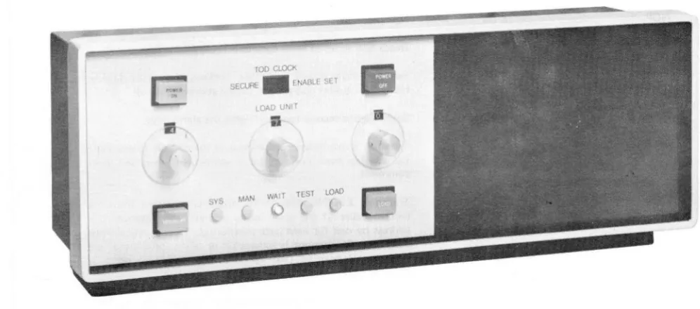
USAGE METERING
System and maintenance meters are located in the system console next to the console processor. Which of these meters runs is a function of the mainten-ance key switch. Time is accumulated on the system meter when the switch is in the system position and the SYSTEM light is on. Time is accumulated on the maintenance meter when the switch is in the maintenance position. If there is no check condition in the CPU and the CPU is not in the STOP or WAIT state, or if the channels are active, then the SYSTEM light will be on.
syS
(
TOD CLOCK
SECURE. ENAHLf SET
LOAD UNIT
•
MAN WAlT TEST LOAD
() (
(
FIGURE 11 OPERATOR'S CONTROL PANEL
[image:23.613.48.546.311.531.2]OPERATOR'S CONSOLE
PROGRAMMING
For 3066 emulation the system console CRT screen
will display 35 lines of 80 characters each. Data may be read from or transmitted to any of these positions on the CRT under program control. Char-acters typed on the keyboard can be placed in any of these positions on the CRT, depending upon the location of the cursor.
The screen is addressed by a two-byte buffer field and a two-byte cursor address field. The first byte in both address fields gives the, line number (0 to 34); the secone! byte' gives the position within the line (0. to 79). This form of address is used to control where information will be written on the screen from the program, which locations on the screen are to be transferred in response to a. read from the· pro-gram, and where the cursor will be placed for. key-board. entry. A two-byte address . is also. returned to the :program when the cursor position is requested.
The following commands control the console:
NOP X'03'
Sense X'04'
Erase X'07'
Alarm X'OB'
Set Buffer Address X'27'
Write X'01'
Read X'06'
Set Cursor X'OF'
Read MI X'OE'
Lock Keyboard X'67'
No operation.
Reads two bytes of sense data (see Table 1 ).
Sets the entire screen to blanks, removes the cursor display, resets CRT buffer address and cursor address to zeros.
Sounds a one·second tone and lights the alarm key.
Transfers a two-byte screen address to the console to designate the starting byte position for a subsequent Read and Write command.
Transmits EBCDIC data to be displayed, starting from the current value of the CRT buffer address, and advances this address by one for each byte transferred. The operation stops when the CCW count is exhausted or when 2S00 bytes are
written. If position (34, 79) is reached, position (0, 0) is
written next.
Transfers data from the screen to the program, starting from the current CRT buffer address, and continues until either the CCW count is exhausted or the byte at the current cursor position is transferred.
Transfers a two-byte address to the console to indicate the screen position at which the cursor should be displayed. If the cursor was not previously displayed and the keyboard was disabled, it can now be used to enter data onto the screen.
Usually issued in response to an attention interruption caused by either the "ENTER" or the "CANCEL" keys, this com-mand returns three bytes of information to the program. The first and second bytes are the current cursor address; the third byte indicates which key was pressed (X'SO') for "ENTER" and X'40' for "CANCEL").
TABLE 1 SYSTEM CONSOLE SENSE DATA
There are a few functional differences between the operation of the Amdahl 470V/6 system console in 3066 emulation as explained above and the opera-tion of the 3066 system console. The following should be noted if exact compatibility is a require-ment:
The 3066 keyboard has both upper and lower case alphabetic input even though the CRT displays only upper case. The Amdahl 4 70V /6 system console has only upper case alphabetic input.
[image:25.612.47.570.48.324.2]APPENDIX A:
MODEL-DEPENDENT FUNCTIONS
The Amdahl 4 70V /6 System and the IBM System/370 are compatible within the constraints of System/370 architecture as specified in the Principles of Operation. This specification requires machine compatibility except in the following cases:
Programs relying on model-dependent data, such as the contents of logout areas
Time-dependent programs that rely on instruction or CCW execution times
Programs that cause deliberate machine checks
INSTRUCTION SET DIFFERENCES
Two instructions have model-dependent results on the Amdahl 470V/6. They are:
STORE CPU ID (STIDP). This instruction causes certain model-dependent data to be stored at the double word addressed by the second operand address. In the Amdahl 470V/6 the version code field is reserved (bits 0-7). A unique serial number is stored in bits 8-31. The hexadecimal number 0470 is stored in the model number field (bits 32-47). Bits 48-63 are stored as zeros since the Amdahl 470V/6 performs the standard machine check extended logout to the memory of the console processor.
STORE CHANNEL ID (STIDC). Channel de-pendent data is to be stored at location 168. Since the 4 70V 16 channel type is implicit in the CPU model, zeros are stored in the channel model number field. The remaining fields (type and length) follow standard conventions.
CPU LOGOUT AREAS
Fixed CPU logout areas are assigned for storage of machine check logout information. Machine check logouts are the result of or associated with a machine error and result in storing model-dependent infor-mation.
FIXED LOGOUT AREA
The 104-byte area starting at location 248 is the fixed logout area. The Amdahl 470V/6 uses only the first 12 bytes of this area for fixed logout information. The failing storage address occupies the word starting at location 248; the region code is assigned to the two words starting at location 252. The remainder of the area, locations 260-351, is reserved.
The failing storage address (FSA) indicates the storage location or block that caused a correctable storage, an uncorrectable storage, or an uncorrectable key error. For a correctable storage error, bits 0-3 of the FSA contain the failing bit address; bits 8-31 contain the failing byte address. When an uncor-rectable storage error is detected, bits 8-31 of the FSA may point anywhere within the failing 16-byte ECC block. When an uncorrectable key error is detec-ted, bits 8-31 of the FSA may point anywhere within the failing 2048-byte protection block. In the case of multiple errors, the FSA may point to any one of the failing locations. In some cases an FSA cannot be stored. When this occurs, the FSA valid bit in the machine check interrupt code (MCIC) is set to zero. (The MCIC is discussed under machine checks).
c c
CD 0 &.2
CJI'-....
o
~ Source....
.....
Source o ~
.. 0
Bit 0....1 Bit
(1)....1
252 0 I-Unit Pipeline Control Error 256 0 E-Unit Multiplier Byte Parity Error
1 E-Unit Condition Code Error 1 E-Unit Byte Adder Input 1 Parity Error
2 E-Unit LUCK1 Byte 0 Parity Error 2 E-Unit Byte Adder Input 2 Parity Error
3 E-Unit LUCK1 Byte 1 Parity Error 3 E-Unit Byte Adder Input 3 Parity Error
4 E-Unit LUCK1 Byte 2 Parity Error 4 S-Unit Bypass Error
5 E-Unit LUCK1 Byte 3 Parity Error 5 S-Unit TLB Key Parity Error
6 E-Unit LUCK2 Byte 0 Parity Error 6 S-Unit TLB Logical Address Parity Error
7 E-Unit LUCK2 Byte 1 Parity Error 7 S-Unit RAR Parity Error
253 0 E-Unit LUCK2 Byte 2 Parity Error 257 0 I-Unit Result Byte 0 Parity Error
1 E-Unit LUCK2 Byte 3 Parity Error 1 I-Unit Result Byte 1 Parity Error
2 E-Unit Multiplicand Byte 0 Parity Error 2 I-Unit Result Byte 2 Parity Error
3 E-Unit Multiplicand Byte 1 Parity Error 3 I-Unit Result Byte 3 Parity Error
4 E-Unit Multiplicand Byte 2 Parity Error 4 I-Unit EAG Parity Error (DA)
5 E-Unit Multiplicand Byte 3 Parity Error 5 I-Unit EAG Parity Error (CI)
6 E-Unit Adder High-Input Phase Error 6 I- Unit Instruction Stream Entrance Parity Error
7 E-Unit Adder Low-Input Phase Error 7 I-Unit Store Data Parity Error
254 0 S-Unit Search Error 258 0 S-Unit Address Translation Error
1 S-Unit Compare Register Parity Error 1 S-Unit Channel Request
2 S-Unit Tag Key Parity Error 2 C-Unit I/O Address Parity Error From I-Unit
3 S-Unit Tag ID Parity Error 3 Reserved
4 S-Unit Store Data Parity Error 4 C-Unit Error on CSW Store
5 Main Store Read Address Parity Error 5 Reserved
6 Main Store Key Write Parity Error 6 Reserved
7 Main Store Write Address Parity Error 7 Reserved
,
255 0 S-Unit Tag Control Parity Error 259 0 E-Unit Multiplier Residue Error
1 S-Unit Move Out Data Parity Error 0 1 E-Unit Adder Residue Error
2 S-Unit Move Out Data Parity Error 1 2 I-Unit Instruction Stream Exit Parity Error (OS)
3 S-Unit Move Out Data Parity Error 2 3 S-Unit TLB Valid or 10 Error
4 S-Unit Move Out Data Parity Error 3 4 I- Unit Control Register Bytes 0 -1 Parity Error
5 S-Unit Primary (1)/ Alternate (0) Buffer 5 I-Unit Control Register Bytes 2 -3 Parity Error
6 S-Unit Primary (1 )/Alternate (0) TLB 6 I-Unit PSW Bytes 0 -11 Parity Error
[image:28.614.30.556.125.708.2]7 S-Unit Translation Register Segment/Page 7 Reserved I
EXTENDED CPU LOGOUT
A machine check extended logout (MCEL) is per-formed by the console processor based on the setting of control register 14 bit 1, the synchronous MCEL mask. If the bit is on and a condition occurs that would normally cause an extended logout, the logout information is stored in the console processor.
The console processor detects the MCEL situation and performs a logout by scanning out all pertinent CPU latches to its own memory. This information can later be examined by a program in the main pro-cessor by issuing a special Diagnose instruction. After the console logout, the main processor is re-started to allow the CPU to continue its normal oper-ation. If the console is not operational, the CPU is restarted by a time-out function and the MCEL is not performed. The CPU is informed of this action on the subsequent Diagnose.
Because MCEL data is saved in the console processor, the machine check extended logout area (location 512 and above) is not used by the Amdahl 470V/6. Control register 15, which normally contains the MCEL address, is not implemented and stores as all zeros.
The Diagnose instruction (operation code x'83 ') provides a means of communication between the CPU and the console processor for diagnostic and main-tenance purposes. Because the operation of the Diagnose instruction may differ depending on the engineering change level of a particular system, documentation of this instruction is not provided in this manual.
MACHINE CHECKS
Extensive checking facilities are implemented in the Amdahl 470V/6. These include parity checking of instructions, registers and data, arithmetic checking of execution functions and effective address gen-eration, and checking for certain illegal control sequences. When processing damage is detected, an
MACHINE CHECK CONDITIONS
A machine check condition is recognized for an un-correctable error. A machine check condition is generated whenever an instruction or data with in-valid parity is fetched, an arithmetic function is improperly performed, or invalid parity on the protection key makes it impossible to establish whether protection applies. Certain invalid control sequences can also cause a machine check condition. A machine check condition can be generated when instructions or data with invalid parity are fetched and before they are used.
If storage and registers contain valid information a machine check condition will be caused only by a machine malfunction, and never by an invalid instruc-tion or data. If an unavailable component is speci-fied the appropriate program, 110 interrupt or condition is set; a machine check condition is not generated.
A malfunction detected by the S-Unit during an 110 operation causes an external damage machine check condition. When the 110 operation is a fetch of a CCW or data, the malfunction is reported in the channel status word (CSW). When data is stored by the channel and a malfunction is detected in the S-Unit after status has been returned to the C-Unit, the CSW does not report the error. When the channel detects bad parity on an input operation, good parity is forced to the S-Unit and a channel data check is reported in the CSW.
An external 110 equipment malfunction detected in :the channel is indicated in a CSW and not treated as a machine check condition. The error is reported as an 110 interrupt.
storage errors, storage key parity errors, and internal CPU data transfer errors that are unretryable are
con-sidered hard machine checks. These conditions may
result in termination of the current instruction or
loss of interrupts.
MACHINE CHECK INTERRUPTS
The machine check interrupt reports an equipment malfunction and supplies information about the
location and nature of the malfunction. Actions taken by the Amdahl 4 70V /6 System in machine
check condition are summarized in Table 3.
A soft machine check occurs after an instruction,
including any associated SVC or program
inter-ruption, has completed. This is the same point at which an I/O interrupt occurs. Two classes of soft machine checks are retryable errors and
cor-rected errors. A retryable error starts re-execution
of the problem instruction; a corrected error is
SOFT MACHINE CHECK
CORRECTED
RETRIED
HARD MACHINE CHECK
UNCORRECTED
UNRETRYABLE
1 AS APPROPRIATE
MCIC STORED YES YES YES YES SYS DMG 0 0 0 *
t 1 IF NOT PAST RETRY THRESHOLD; ELSE = 0
[image:30.612.36.557.300.709.2]** ;;,
TABLE 3
IF AVAILABLE
AMDAHL 470V/6 MACHINE CHECK ACTION
0 3
BIT
CS
7
FUNCTION
Check stop
PROC DMG
0
0
*
handled as a soft machine check (so far as point of
interruption is concerned).
A hard machine check immediately inhibits further updating of machine state, including storage and
registers, and points the instruction counter to the instruction farthest along in the pipeline. This
action is taken immediately, before the end of an
instruction, but still could have been caused by a part of the execution of any of the instructions in
the pipeline (up to six).
With the exception of processing of machine check
extended logouts and the associated
nonimple-mentation of control register 15, the Amdahl 4 70V /6 fully implements standard machine check handling
as defined in the Principles of Operation. rhe signi-ficant bits of control register 14 and the machine check interrupt code (MCIC) for the Amdahl 470V /6
are detailed in Figures 12 and 13.
SYS REC
0 0
GPRs FSA
BACKUP STORED STORED
0 ** **
0 ** **
t ** **
0 ** **
31 REG CODE STORED NO ** ** ** SL IL
Synchronous machine check extended logout channel
I/O extended logout mask
RM
Recovery report maskI I I I r I I I
SPSTCE D
Dp,RDDD IGI
0 6 7 8 14
BIT FUNCTION
SD System damage
PD Processor damage
SR System recovery
TD Timer damage
CD Timing facilities damage
ED External damage
DG Degradation
B Backed-up
D Delayed
SE Storage error uncorrected
SC Storage" error corre,cted
FIGURE 13 MACHINE CHECK INTERRUPT CODE (MCIC)
HARDWARE DIAGNOSTIC MODE
When a check stop or some other condition occurs that requires manual intervention, a diagnostic mode (hardware command or maintenance mode) may be entered from the operator's console. Data may then be stored or displayed, and the machine state may be
otherwise changed from the console. Further details on these procedures are found in Appendix D.
BIT
KE
WP
MS
PM
IA
FA
FP
GR
CR
TR
CC
IW 1M 'pil IF I PSMAA
20 24 272829 31
4647 63
FUNCTION'·
Key in storage error corrected
PSW EMWP valid
PSW masks and key valid
Program masks and CC valid
Instruction address valid
, "'>,·c·
Failing storage address valid
Floating point registers valid
General purpose registers valid
Control registers valid
CPU timer valid
[image:31.616.49.570.47.414.2]APPENDIX B:
INSTRUCTION TIMING ESTIMATES
The timing formulas given below were derived through engineering analysis of system documen-tation. Because the Amdahl 470V/6 is complex and has many overlapping functions, the formulas make certain assumptions and are not completely com-prehensive. While efforts were made to assure accu-racy of data included, it is possible that errors have been made and these timings are not warranted to be correct. Future system measurement and analysis are planned to further modify and refine the for-mulas. In addition, Amdahl Corporation reserves the right to make changes and enhancements that may alter the timings as herein presented.
The following table lists the number of cycles required for execution of each of the instructions of the Amdahl 470V/6. Included with some of the formulas are variables that affect execution; these are explained at the end of the table. In addition, those instructions indicated by an asterisk are suf-ficiently complex that only imprecise estimates of their execution times are given in the table (see "Special Timing Formulas"). Because of the parallel, complex architecture of the Amdahl 470V/6, care should be exercised in the use of these formulas. As is readily determined from an analysis of the special terms in many instructions, the execution times for a given instruction can often vary greatly.
EARLY CONDITION CODE
SETTINGS
The timing estimate for the conditional branch instruction depends on how early the condition code becomes valid. Condition code setting instructions have a term in the "CC Set" column that specifies the number of cycles to add to the execution of an associated conditional branch instruction. An "N" indicates that the speed of the condition code depends on whether the instruction operands are normalized. This term is further explained under "Special Timing Formulas".
RETRYABLE INSTRUCTIONS
The given digits and symbols indicate thresholds beyond which the instruction b"ecomes nonretryable. The notation "SI" indicates that the instruction is not retryable after a store in the instruction stream. The absence of any digit or symbols indicate the in-struction is completely retryable. Other cases of non-retryable instructions include threshold numbers. The BAL instruction has a threshold of two cycles.
TIMING FORMULAS
INSTRUCTIQN FORMAT II/INEMO"!IC CCSET RTRY PERFORMANCE
AQg
RR AR Q 2Add RX A 0 2
:f
Add Decimal 1)1) AP .0 E-2R 13-41 + 54Ac;ld Halfword RX AH Q
2
Add Logical RR AlR 0 2
Add logical RX Al 0 2
Add "!ormalized (Extended) RR AXR 0 2 15
+
3*RC t AL + ,,!P + PWI;>:f:Add Normaliz!ld (Long) RR ADR N 1 + 2,jRC
+
RRR:f:Add Normali2:ed (Lon!!) RX AI;> N 7 + 2*RC + RRR
:f: Add Normalized (Short) RR AER 1\1 6 + RC
*
Add 1\I0rOla.lizeg (!)hort) RX AE N 6 + RC:f: Add Unnormalized (Lang) RR AWR N 7 + 2*RC+ RRR
:f: Add Unnormalized (Long) RX AW N 7 +2*RC + RRR
:f: Add U!lIlormalized (Short) RR AUR N 6
+
Rc=1= Add Um:l!,umaliz!ld (Shard RX AU N ~ + RC
AND RR NR Q
2
AND RX N 0, 2
AND SI NI Q 2 4+ S1
ANI;> 1)$
NC
() 4 61.. +81
Branch eng l,.ink RR BAlR 2 8 + PWD
Branch and link RX aAl 2 B + OWO
Bra.neh on Condition RR B9R O,(T) 2 + BT*(3-S3) + CeS + 1)3 + l6*BCR
aranch on COndition RX BC O(T) 2
+
BT *(:3-8:31 + CCS + S3Branch
on
Count RR BCTR 2 4 + S3.+ BT*(3-83)Branch on Ct;lunt RX !'ICT
2
4 + S3 + BT*(3-S3)Branch on I ndex High RS BX/-I 2 6 + S3 + BT*(3,,-S3)
t:3ranel1 on Index loW
or Equal RS BXlE 2 6 + S3 + BT*(3-83)
:f: Clel;lr I/O S eLRIO 0 2 26. + CURT
Compare RR CR 0 2
Compare RX C 0 2
Compare and Swap RS CS 24
:f: Compare Decimal SS CP 0 13-47 + S4
Compare Double & Swap RS CDS 32
Compare Halfword RX CH 0 2
Compare Logical RR ClR 0 2
Compare logical RX CL 0 2
Compare logical SI CLI 0 2 2
Compare logical SS CLC 0 4*W + 4*X + 4*Y
Compare logical Characters
Under Mask RS CLM +2 2
Compare logical long RR ClCL 0 EB 36 + 4*W + 4*X + 4*Y
Compare RR CDR +2 3 + 3*UN + RRR
Compare RX CD +2 3 + 3*UN + RRR
Compare RR CER +2 3 + UN
Compare RX CE +2 3 + UN
INSTRUCTION FORMAT MNEMONIC CCSET RTRV PERFORMANCE
Divide RR DR 50
Divide RX D 50
*
Divide Decimal 5S DP E-2R 31~2036 + S4Divide (Long) RR DDR 64 + PN1 + PN2 + DP5
Divide (Long) RX DD 64 + PN1 + PN2 + DPS
Divide (Short) RR DER 27
Divide (Short) RX DE 27
Edit 5S ED 0 4 6*L + S1
Edit and Mark SS EDMK 0 4 6*L + 6
Exclusive OR RR XR 0 2
Exclusive OR RX X 0 2
Exclusive OR SI XI 0 2 4 + S1
Exclusive OR 5S XC 0 4 6*L + S1
Execute RX EX 24 + TGE
*
Halt I/O 5 HIO 0 2 26 + CURT*
Halt Device 5 HDV 0 2 26 + CURTHalve (Long) RR HDR 6 + RRR
Halve (Short) RR HER 4
Insert Character RX IC 2
Insert Character Under Mask RS ICM 0 9
Insert PSW Key 5 IPK 2
*
Insert Storage Key RR 15K 23_75Load RR LR 2
Load RX L 2
Load Address RX LA 2
Load and Test RR LTR 0 2
Load and Test (Long) RR LTDR +1 2 + RRR
Load and Test (Short) RR LTER 0 2
Load Complement RR LCR 0 2
Load Complement (Long) RR LCDR +1 2 + RRR
Load Complement (Short) RR LCER 0 2
Load Control RS LCTL 2 6 + 2*R + 16*RIF
Load Halfword RX LH 2
Load'(Long) RR LDR 2 + RRR
Load (Long) RX LD 2 + 53 + RRR
Load Multiple RS LM 2 2*R + 2
Load Negative RR LNR 0 2
Load Negative (Long) RR LNDR +1 2 + RRR
INSTRUCTION FORMAT 'MNEMONIC CCSET RTRY PERFORMANCE
Move SI MVI SI 2 + S1
Move SS MVC 6 6 + MV + S1 + 4*WB
Move Long RR MVCL 0 2 45 + 4*W + 4.BPE + 16*PE
Move Numerics SS MVN 4 6*B + 51
Move with Offset SS MVO 4 2 + MVB +S1
Move Zones SS MVZ 4 6*B + S1
Multiply RR MR 7
Multiply RX M 7
:j: Multiply Decimal SS MP E-2R 21-.409 + S4
Multiply RR MXR 2 94 + PN1 + PN2
+
DWDMultiply Halfword RX MH 8
Multiply (Long) RR MDR 20 + PN1 + PN2 + RRR
Multiply (Long) RX MD 20 + PN1 + PN2 + RRR
I Multiple (Long to Extended) RR MXDR 2 28 + PN1 + PN2/2+ DWD
Multiply (Long to Extended) RX MXD 2 28 + PN1 + PN2/2 + DWD
Multiply (Short) RR MER 8
Multiply (Short) RX ME 8
OR RR OR 0 2
OR RX 0 0 2
OR SI 01 0 2 4 + S1
OR SS OC 0 4 6*L + S1
:j: Pack SS PACK 4 4*B +S1
:j: Purge TLB S PTLB 2 (Nominal)
Read Direct SI RDD 88 + HRT
:j: Reset Reference Bit S RRB 0 2 23 __ 75
Set Clock S SCK 0 6 + 'TODRT
Set Clock Comparator S SCKC 6 + TODRT
Set Program Mask RR SPM 6
Set CPU Timer S SPT 6 + TODRT
Set PSW Key from Address S SPKA 18
:j: Set Storage Key RR SSK SI 156-384
Set System Mask S SSM 2 8 + EC
Shift & Round Decimal SS SRP 0 E-2R 40 + S2
Shift Left Double RS SLDA +2 4 + RRR
Shift Left Double Logical RS SLDL 3 + RRR
Shift Left Single RS SLA +2 2
Shift Left Single Logical RS SLL 2
Shift Right Double RS SRDA +2 3 + RRR
Shift Right Double Logical RS SRDL 2
+'
RRRShift Right Single RS SRA +2
2
Shift Right Single Logical RS SRL 2
:j: Start I/O S SIO 0 2 26 + CURT
:j: Start I/O Fast Release S SIOF 0 2 /26-+ CURT
~---'
Store RX ST SI 2 +-S1 + DWD
:j: Stor~ Channel I D S STIDC 0 2 26 + CURT
Store Character RX STC SI 2 + S1 + DWD
Store Character Under Mask RS STCM SI 4 + S1
Store Clock S STCK 0 SI 22 + TODRT
INSTRUCTION FORMAT MNEMONIC CCSET RTRY PERFORMANCE
Store CPU 10 S STIDP SI 4 + S2 + DWD
Store CPU Timer S STPT SI 6 + 52 + TODRT
Store Halfword RX STH SI 2 + S1 + DWD
Store (Long) RX STD SI 4 + S2 + DWD
Store Multiple RS STM SI 2*R + S2 + DWD
Store (Short) RX STE SI 2 + S1 + DWD
Store Then AND System Mask SI STNSM SI 24
Store Then OR System Mask SI STOSM SI 24
Subtract RR SR 0 2
Subtract RX S 0 2
*
Subtract Decimal SS SP 0 E2 13--47 + S4Subtract Halfword RX SH 0 2
Subtract Logical RR SLR 0 2
Subtract Logical RX SL 0 2
Subtract Normalized RR SXR 0 2 15 + AL + 3*RC + NP + DWD
(Extended)
*
Subtract Normalized (Long) RR SDR N 7 + 2*RC + RRR*
Subtract Normalized (Long) RX SO N 7 + 2*RC + RRR*
Subtract Normalized (Short) RR SER N 6 + RC*
Subtract Normalized (Short) RX SE N 6 + RC*
Subtract Unnormalized (Long) RR SWR N 7 + 2*RC + RRR*
Subtract Unnormalized (Long) RX SW N 7 + 2*RC + RRR*
Subtract Unnormalized (Shorr) RR SUR N 6 + RC*
Subtract Unnormalized (Short) RX SU N 6 + RCSupervisor Call RR SVC 44
Test and Set S TS 0 0 18
*
Test Channel S TCH 0 2 26 + CURT*
Test I/O S TID 0 2 26 + CURTTest Under Mask SI TM 0 2
Translate SS TR 4 5* rB/41 + 2 + 4*B + S1 $
Translate and Test SS TRT 0 2 5* rB/41 + 4*B + 4*M + 4 $
Unpack SS UNPK 4 5* nB-1)/21 + 4 + UPK* (B-1) $
Write Direct SI WRD 2 86
Zero and Add SS ZAP 0 E-2R 13 + 5*WL + S4
:j: More precise timing may be obtained for these instructions by referring to the section entitled
"Special Timing Formulas" in this appendix.
e
i,.,
PriMMA!"LEGEND
FOR
TIMING FORMULAS
SYMBOL
AL
EXPLANATION
Alignment exponent difference
<
8 = 92:8,<16 =8 2: 16
=
7B Number of bytes moved, packed/unpacked, or
translated.
BCR If Bl = F and R2 = 0
then BCR = 1; otherwise, BCR =0.
BPE The number of bytes (less than 4) remaining
to be accessed by either the fetch or store field for a given page.
BT Branch taken = 1; otherwise = O.
CCS Condition code setting factor. The value is
given in CC Set column.
CURT Channel unit release time. For detailed
ex-planation of this term, see the "Special Timing Formulas" section of the Appendix.
D DPS DWD EC HRT L L2 M ME MV
Number of significant decimal digits.
= 1 if dividend preshiftrequired, else=O.
DWD = 1 if a double word result instruction
precedes subject instruction.
In EC mode, EC
=
16.Hold response time. The value ranges from 0 to 33 with equal probability; the average is 16.5.
In SS-type instructions L = the length in bytes of the first operand.
In SS-type instructions L2 = the length in bytes of the second operand.
equals 1 if any other than last byte to be tested is nonzero; otherwise, M = O.
ME = 46 cycles if the event is monitored.
equals:
No overlap or overlap> 32 bytes or
both operands on word boundary 4*W
3 bytes
<
overlap::: 32 bytes or both operands not on word boundary1 byte
< overlap::: 3 bytes
overlap = 1 byte
5*W
4*B
6*B
SYMBOL EXPLANATION
MVB equals:
N NP Nl PE PNl PN2
No overlap or overlap t= 1 byte 4*B
overlap = 1 byte 6*8
= 1 if sign negative; otherwise = O.
Post normalization.
Leading zero digits ::: 6 = 6
>
6 ::: 14 = 10>14 = 7
= 1 if first operand's sign is negative; else
=
0When the fetch or store field reach a page
boundary, PE
=
1. .= 2 if prenormalization required on operand
one, else = O.
== 2 if prenormalization required on operand
two, else = O.
R Number of registers to be loaded or stored.
R I F R I F = 1 . if instruction modifies CRO or CR 1 ; or
if PER is enabled and instruction modifiesCR9,
CR10 or CR11. Otherwise, RIF = O.
RC Recomplement.
=
1 if recomplementationrequired; otherwise = O.
RN = 1 if rounding required, else = O.
RRR If the instruction immediately following the
subject instruction has a single word operand,
Sl
then
-RRR = 0 if E:::4 1 if E
=
3 2 if E = 2where E is the number of execution cycles in that that instruction. If the instruction immediately following the subject instruction has a double word operand, then
RRR = 0 if E:::5 1 if E
=
4 2 if E=
3 3 if E=
2Sl
=
2 if M=
6 = 1 if M = 7=
0 if M=
8SYMBOL
S2,S3
EXPLANATION
S2 = 0 if P = 8
= 1 if P = 7
= 2 if P = 6
= 3 if P = 5
= 4 if P = 4
S3 = 0 if P = 6
= 1 if P = 5
= 2 if P = 4
where P equals the number of execution cycles attributable to the two words of the instruction stream following the instruction of interest.
S4 Use S3 if both operands total less than five
bytes; otherwise, use S2.
TGE Target instruction execution time.
TODRT Time·of-day response time. The value
ranges from 1 to 30 with equal probability; the average is 15.5.
UN = 1 if either operand unnormalized;
otherwise, = O.
UPK equals 1 if overlap present.
W Number of words compared or moved.
WB For L
>
64, WB equals the number of byteswhich must be moved to have the store field
aligned on a word boundary. For L
<
64,WB=Q
WL Number of words in the longer operand.
X In logical comparison (CLC, CLCL), X = 1
if an inequality is detected in other than the last word compared; otherwise, X=O.
Y In logical comparison (CLC, CLCL), Y = 1
if an inequality is detected in other than the last
SPECIAL TIM ING FORMULAS
Several instructions were flagged in the main list, since only a wide variation in execution times could be given there. More precise estimates of execution times can be determined using the tables and for-mulas below.
ADD DeCIMAL (AP)
1-4
SIGNS ALIKE 13
SIGNS DIFFERENT 15
COMPARE DECIMAL (CP)
1-4
SIGNS ALIKE 15
SIGNS DIFFERENT 13
CURT
Channel response time depends on broad variety of conditions. The formulas given below assume no interference of other channels with an I/O instruc-tion issued to a channel. All values are machine cycles except values of variable C.
Length in Bytes of the Longer Operand
5-8 9-12 13-16
23 33 43'
25 36 47
Length in Bytes of the Longer Operand
5-8 9-12 13-16
25 36 47
23 33 43
Channel Idle/Subchannel Idle
Maximum Maximum Syte &
Instruction Minimum Selector Block Multiplexer
SIO 246 + SS 261 + SS 261 + SS
SIOF 36 51 51
TIO 230 + SS 245 + BS 245 + SS
TCH 4 19 19
STIDC 20 35 35
HIO 278 + SS 293 + SS 293 + SS
HDV 326 + SS 341 + BS 341 + SS
Channel Idle/Subchannel Working
Maximum
Instruction Minimum Selector
SIO 20 35
SIOF 20 35
TIO 20 35
TCH 4 19
STIDC 20 35
HIO 274 + BB 289 + BB
HDV 274 + BB 289 + BB
CLIO 20 35
Channel Idle/Subchannel Interrupt Pending
Maximum
Instruction Minimum Selector
TIO 36 51
Channel Working
Maximum Instruction Minimum Selector
SIO 4 19 +A
SIOF 4 19 +A
TIO 4 19 +A
TCH 4 19 +A
STIDC 4 19 +A
HIO 20 35
HDV 20 35
CLIO 4 19 +A
Where:
A
=
delay due to reselection during chaining of a working subchannel.Min = 0 cycles Max
=
210 cycles + BB C=
120 to 135 microsecondsMaximum Byte Mpx in Burst Md
19 + C 19 + C 19 + C 19 + C 19 + C 35+C 35+C 19 + C
Maximum Byte & Block Multiplexer
35 35 35 19 35 289,+ BB 337 + BB 153
Maximum Byte & Block Multiplexer
99
Maximum Block Mpx
19 + A 19 +A 19+A 19 +A 19 + A
DiVIDE DECIMAL (DP)
If L2
<::
3; formula is 20 +(5
+
4Q)N
+ tRWif
3
<t
LZ,
formula is27
+ (9 +6Q)N
+ tRWWhere Q equais the average value of the quotient digits plus
i;
N equals the nurnber of quotient digits;
RW
equals the number Of words of resuh.FLOATING POINT OPERATIONS;.;... EARLY CONDITION CODE SETTING FACTOR
<