A Study on FPGA Based Digital Modulators
Akanksha Sinha
1, Piyush Lotia
2M.E. Scholar [VLSI Design], Dept. of ETC, Shri Shankaracharya Technical Campus, Bhilai, Chhattisgarh, India 1
Associate Professor, Dept. of E&I, Shri Shankaracharya Technical Campus, Bhilai, Chhattisgarh, India 2
ABSTRACT:This paper presents a study on different digital modulation techniques based on FPGA and their Bit Rate Error. Digital modulation represents the transfer of the digital bit stream from the transmitter to the receiver via the analog channels. The information signal modifies one or more carrier parameters, leading to shift keying techniques during the modulation process. Various DSP based data compression, encoding/decoding algorithms, and noise filtering techniques have been developed to achieve effective and efficient data transmission with the help of FPGAs for hardware implementation. Modulators were designed using VHSIC (Very High Speed Integrated Circuit) Hardware Description Language (VHDL) was realized on high speed FPGA (Field Program Programmable Gate Array). Data rate transfer is fairly important in wireless communication systems. BER (Bit Error Rate) of different digital modulators was compared. From literature survey it was found that design employs the minimum number of blocks necessary for achieving different digital modulation. The functionality of these digital modulators will be demonstrated through simulations using Xilinx 13.2.
KEYWORDS: BASK, BPSK, BFSK, QPSK, and FPGA.
I.INTRODUCTION
The choice of digital modulation scheme will significantly affect the characteristics and performance of a communication system. The objective of a digital communication system is to transport digital data between two or more nodes. This is usually achieved in radio communication by adjusting a physical characteristic of a carrier (sinusoidal), the frequency, phase, amplitude or a combination of it. This is performed in real systems with a modulator at the transmitting end to impose the physical change to the carrier and a demodulator at the receiving end to detect the resultant modulation on reception.
Field-programmable gate arrays (FPGAs) are semiconductor devices containing programmable logic elements (LEs) and a hierarchy of reconfigurable interconnects to realize any complex combinational or sequential logic functions. Today’s FPGAs consist of configurable embedded static random-access memories (SRAMs), high-speed input/output (I/O) elements, high-speed transceivers and even hard-embedded processors [9]. FPGAs are widely used in different applications, such as motor controllers [10], neural network implementations [1, 3], finite-impulse-response (FIR) filter realization [11, 12], fuzzy-logic controllers [13], etc. In this paper, basic block diagram and implementation of digital modulators using FPGAs has been studied.
II.REVIEW OF RELATED WORK
This section presents a brief review of some of the most recent literature published in the related field.
shows improvement in induction load characterization. For designing of inductors and power converter impedance of this type of large signal is used, it also provide real time measurement of parameters. S.O. Popescu et al [7] proposed a method to design BPSK modulator and Demodulator using Matlab/Simulink environment and implement it to FPGA Spartan 3E kit. The modulator and demodulator were integrated into two different boards, having local clock oscillator of the board of 50 MHz which corresponds with a period of 20ns. The BPSK carrier frequency is 31,250 kHz. This design is suitable for propagation and to minimize memory utilization. Mehmet Sonmez, Ayhan Akbal [8] presented simulation results of binary frequency shift keying (BFSK) and binary phase shift keying (BPSK) modulation techniques in FPGA complier. They proposed both the modulation techniques in low power consumption systems. In addition, these modulation techniques are used high speed systems. Also, BPSK and BFSK modulations are compared to bit error rate (BER). BPSK modulation technique has BER low than BFSK modulation in AWGN channel. Modulators were designed using FPGA complier (Quartus II 9.1). In Quartus II complier, results of simulation are observed using vector waveform file.
III. DIGITAL MODULATORS
A. BASK Modulator
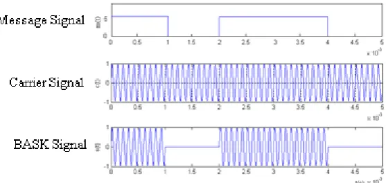
In a BASK (binary amplitude-shift keying) modulator, the amplitude of the carrier (sinusoidal) signal is changed according to the message level (“0” or “1”), while keeping the frequency and phase constant. If transmitting data is 1, BASK modulated signal is carrier signal. When transmitting data is 0, BASK modulated signal is 0. In modulation
process the data bits are multiplied with a carrier signal and then modulated signal is created.
S(t) = Ac Sin(2𝜋𝑓𝑐𝑡) ; if symbol = 1
S(t) = 0 ; if symbol = 0 (1)
Fig. 1 A block diagram of BASK modulation
Fig.1 shows a block diagram of BASK modulator. The multiplier output is modulated by binary code. This NRZ level encoder converts the input binary sequence to the signal suitable for product modulator.
Fig. 2 The modulating-signal (message) and the BASK signal waveform
B. BPSK Modulator
In a BPSK (binary phase-shift keying) modulator, the phase of the sinusoidal carrier signal is changed according to the message level (“0” or “1”) while keeping the amplitude and frequency constant. If transmitting symbol is 1 then beginning of BPSK modulated signal’s period is positive values. But if transmitting signal is 0, beginning of BPSK modulated signal’s period is negative values.
S(t) = Ac Sin(2𝜋𝑓𝑐𝑡) ; if symbol = 1
S(t) = -Ac Sin(2𝜋𝑓𝑐t) ; if symbol = 0 (2)
Fig. 3 A block diagram of BPSK modulation
In Fig. 3, the block diagram of BPSK modulator is shown. Binary data is converted to binary code bipolar format, then binary code bipolar format signal is multiplied carrier signal. Thus, BPSK modulated signal is created.
Fig. 4 The modulating-signal (message) and BPSK signal waveforms
Fig. 4 shows the message signal, carrier signal and BPSK modulated signal waveforms.
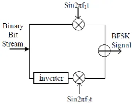
C. BFSK Modulator
In a BFSK (binary frequency-shift keying) modulator, the frequency of the carrier signal is changed according to the message level (“0” or “1”) while keeping the amplitude and phase constant.
S(t) = Ac Sin(2𝜋𝑓1c𝑡) ; if symbol = 1
S(t) = Ac Sin(2𝜋𝑓2c𝑡) ; if symbol = 0 (3)
Fig. 5 shows the block diagram of BFSK modulator. Binary bit stream is multiplied with the carrier signal. Same bit stream was inverted and multiplied with carrier signal. After addition of both the signals we get BFSK signal.
Fig. 6 The modulating-signal (message) and BFSK signal waveforms
Fig. 6 shows the message signal, carrier signal and BFSK modulated signal waveforms.
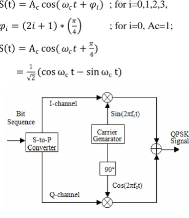
D. QPSK Modulator
QPSK modulation is based on Phase modulated. Namely, for each symbol, different phase data is sent to channel. Each symbol consists of two bits. These bits are modulated in I channel and Q channel. For I channel carrier signal is used sinus, for Q channel carrier signal is used cosines. For QPSK modulation, there are four cases. These cases are 00, 01, 10 and 11. For each case, QPSK signal is created using signal of different phase. These phases are 45°, 135°, 225° and 315°. Hence, in contrast to binary modulation techniques such as BPSK (Binary Phase Shift Keying), BFSK (Binary Frequency Shift Keying), BASK (Binary Amplitude Shift Keying), QPSK modulation technique is a fast modulation technique.
The QPSK modulation signals are defined as
S t = Accos( 𝜔𝑐𝑡 + 𝜑𝑖) ; for i=0,1,2,3, (4)
In equation (4), 𝜑𝑖= 2𝑖 + 1 ∗
𝜋
4 ; for i=0, Ac=1;
S t = Accos( 𝜔𝑐𝑡 + 𝜋 4)
= 1
2(cos ωct − sin ωct) (5)
Fig. 7 A block diagram of QPSK modulation
Fig. 8 A QPSK modulated signal
The QPSK modulated signal with I channel and Q channel is shown in figure 8.
IV.DIGITAL MODULATORS BASED ON FPGA
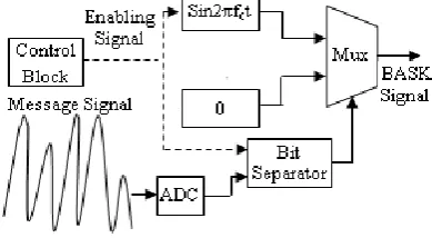
A. FPGA Based BASK Modulator
BASK based on FPGA application can be successfully simulated in Xilinx ISE 13.2. Also, both modulation and demodulation can be implemented on FPGA. So, modem based on FPGA is created. The block diagram of the BASK system implemented on the FPGA is illustrate in fig.9.
Fig. 9 BASK system implemented on FPGA
B. FPGA Based Design of BPSK Modulation
BPSK modulated signal can be created by simulator. The block diagram of BPSK Implemented on FPGA is shown in Fig.10. Using ADC, message signal is converted digital signal. Thus, in FPGA, the signal can be processed and FPGA based BPSK modem can be created. The bit separator separates output of ADC one by one in 14 bits. Bit Separator will be created using Very high speed integrated circuit Hardware Description Language.
C.FPGA Based Design of BFSK Modulation
Using Xilinx ISE simulator, BPSK modulated signal can be created. Real time logical circuits have high clock frequency, so FPGA operates very fast and received data are processed in real time. This advantage is very important for wireless communication systems because data transfer rate is virtual value in mobility. Figure 11, shows the block diagram of FPGA-based BFSK modulation.
Fig. 11 BFSK system implemented on FPGA
D. FPGA Based Design of QPSK Modulation
Before design is created on FPGA, block diagram of FPGA-based design is realized and a possible algorithm is produced. Almost all the designs are controlled using a control block. Used FPGA-based QPSK modulator algorithm is the fastest FPGA-based QPSK modulator, because one digital sample is transmitted using only one enabling signal (created by control block). Namely, any multiplier or added block is used in this design. Only for one sample of output signal (QPSK modulated signal), MUX is used. The block diagram of QPSK Modulator implemented on FPGA is shown in fig. 12
Fig. 12 QPSK system implemented on FPGA
V.FPGAANDVHDL
VI.BITERRORRATE(BER)
A. BASK and BPSK BER
In an AWGN channel, the BER (Bit Error Rate) decreases approximately exponentially as the SNR (Signal to Noise Ratio) increases [8]. Straight BPSK produces good BER value at the receiver. BPSK transmits symbols at same the rate of BASK Bit error rate of BPSK as the symbol error rate for BPSK is low that of BASK. Bit error rate of BPSK can be shown at equation 6 while bit error rate of BASK can be shown at equation 7.
Pb= Q( 2Eb
N0) (6)
Pb= Q( Eb
N0) (7)
In equation (6) or (7), Eb and No represent average energy per bit and noise power respectively.
Fig 14: BER of BPSK and BASK modulation technique
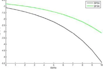
B. BPSK and BFSK BER
In order to performance comparison of BPSK and BFSK, BER of these modulations must be explained. So, error of probability these modulations is evaluate the performance of the detector when the additive noise is white and
Gaussian. BER of BPSK modulation is presented in equation (6). In these equations Eb, N0 are the energy per bit and
noise power respectively. There exists a phase difference of 1800 in BPSK modulation technique. Therefore probability
error can be expressed as shown in equation (6). On the other hand, for BFSK, error probability is presented by equation (7).
C. QPSK BER
QPSK modulation has a good BER performance and is very suitable implementations require 1-2 bps/Hz (bit per second per Hertz) spectrum efficiency and is commonly used in wireless communication [9]. Modulated signal is sent over AWGN (Additive White Gaussian Noise) and afterwards noisy signal is demodulated using FPGA-based complier (Quartus II). But noisy magnitude of AWGN channel is quite low. So, BER (Bit error rate) of this modulator is very low.
VII. CONCLUSION
FPGA implementations of BASK, BPSK, BFSK and QPSK digital modulators can be demonstrated using Xilinx ISE 13.2. The advantages of the implementations are the minimum numbers of digital blocks used for performing digital modulations, integrating ability with modules in FPGA boards, and the controllability of the input signal’s frequencies. In addition, we can demonstrate the hardware implementation of different digital modulation techniques based on FPGA. Also, different performance parameters of modulation techniques will be analysed. it is shown that modulation techniques (BASK, BPSK, BFSK and QPSK) have disadvantage and advantage in simulation and plotting results. It is illustrated that BER of bask high than BER of BPSK. Yet, bit transfer rate of bask is as same as bit transfer rate of BPSK. Comparison of BER over AWGN for BPSK and BFSK was introduced. Besides, it is shown that BPSK modulation technique has BER low than BFSK modulation technique. The implemented FPGA designs are suitable for realization of the digital baseband-modulation. In addition, usage of this kind of implementation for educational purposes in digital communications laboratories or courses clearly emphasizes the correlation between different courses in electronics engineering.
REFERENCES
[1] S. Himavathi, D. Anitha, and A. Muthuramalingam, “Feed forward Neural Network Implementation in FPGA Using Layer Multiplexing for Effective Resource Utilization,” IEEE Transactions on Neural Networks, pp. 880-888, March 2007.
[2] N. M. Botros and M. Abdul-Aziz, “Hardware Implementation of an Artificial Neural Network Using Field Programmable Gate Arrays (FPGA’s),” IEEE Transactions on Industrial Electronics, pp. 665-667, 1994
[3] T. Orlowska-Kowalska and M. Kaminski, “FPGA Implementation of the Multilayer Neural Network for the Speed Estimation of the Two- Mass Drive System,” IEEE Transactions on Industrial Informatics, 7, 3, 2011, pp. 436-445. (2002)
[4] Dhivya Jose, Reneesh C Zacharia , Rijo Sebastian.” A Novel Approach For the Design and Implementation of FPGA Based High Speed Digital Modulators Using Cordic Algorithm” IJEDR | Volume 2, Issue 2 | ISSN: 2321-9939”, 2014
[5] C. Erdoğan, I. Myderrizi, and S. Minaei, “FPGA Implementation of BASK-BFSK-BPSK Digital Modulators” Proceedings of the IEEE Antennas and Propagation Magazine, Vol. 54, No. 2, April 2012.
[6] Oscar Jimenez, Oscar Lucia, LuisA.Barragan, Denis Navarro, Jose I. Artigas, and Isidro Urriza “FPGA-Based Test-Bench For Resonant Inverter Load Characterization” IEEE Transactions on Industrial Informatics, VOL. 9, NO. 3, August 2013
[7] S.O. Popescu, A.S.Gontean and G.Budura, “BPSK System on Spartan 3E FPGA”, SAMI 2012 • 10th IEEE Jubilee International Symposium on Applied Machine Intelligence and Informatics • January 26-28, 2012.
[8] Mehmet SONMEZ1, Ayhan AKBAL “FPGA Based, Low Cost Modulators of BPSK and BFSK, Design and Comparison of Bit Error Rate over AWGN Channel” Gazi University Journal of Science GU J Sci 26(2):207-213 (2013).
[9] Chia-Liang Liu and Kamilo Feher, "π/ 4 QPSK MODEMS for Satellite Sound/Data Broadcast Systems", IEEE Transactions on Broadcasting, Vol. 37, No. 1, March, 1991.
[10] Alecsa, and A. Onea, “Design, Validation and FPGA Implementation of a Brushless DC Motor Speed Controller,” Proceedings of the 17th IEEE International Conference on Electronics, Circuits, and Systems (ICECS), , pp. 1112-1115, December, 2010
[11] P. K. Meher, S. Chandrasekaran, and A. Amira, “FPGA Realization of FIR Filters by Efficient and Flexible Systolization Using Distributed Arithmetic,” IEEE Transactions on Signal Processing, pp. 3009-3017, 2008
[12] K. N. Macpherson and R. W. Stewart, “Rapid Prototyping – Area Efficient FIR Filters for High Speed FPGA Implementation,” IEEE Proceedings ─ Vision, Image and Signal Processing, 153, pp. 711-720.June 2006
[13] B. Leung, VLSI for Wireless Communication. Englewood Cliffs, NJ:Prentice-Hall, 2002 [14] Pedroni, A.,V., “Circuit design with VHDL”, MIT press, England, 2004