Available online:
https://edupediapublications.org/journals/index.php/IJR/
P a g e | 806Performance Analysis of High Step up Resonant Converter Based PV fed
Induction Motor Drive
Sakinala Govardhan
Assistant Professor, Department of EEE, CITS –Warangal.
Abstract- Solar energy is one the most available energy nowadays. This paper deals with the power extracted from sun using PV panel. This paper proposes a new low cost converter- inverter drive system for induction motor. In those places, the unavailability of electric power rules out through conventional systems. Use of photovoltaic energy is one of the solution for this problem. Voltage from the PV array is the input to the converter. In the converter-inverter system, it proposes a Dual Inductor Converter consisting of a resonant tank, voltage doubler rectifier which act as a DC-DC boost converter. The output of the converter system is given to the inverter system. SPWM control is used to trigger the IGBT’s in the inverter. But the voltage from the PV cell is not constant which varies according to the solar radiation. MPPT control is provided; it maximizes the power output from a PV module or array with varying operating conditions, and therefore maximizes the system efficiency. To obtain the maximum power extracting efficiency perturb and observe maximum power point tracking algorithm is introduced for the controlling of converter. The system is simulated in Matlab/Simulink.
Index Terms-Renewable energy, resonant converter, soft switching, voltage step-up, voltage stress.
I. INTRODUCTION
Solar energy is one of the renewable source of energy. This paper deals with the design of improved resonant source inverter which is used for induction motor drive. The input to the inverter is provided by PV cell which obtains light energy from the sun. As space vector pulse width modulation is used it has less THD which can be driven for motors. In addition to the cost of installation and maintenance another drawback is the problem of battery replacement [1]. The boost stage between PV module and the motor can be avoided by the use of low voltage dc motor. But the disadvantages come like it is not suitable for application in isolated areas, lower efficiency and higher maintenance cost compared to induction motor.
Generally, single inductor boost converters were used for improving the input voltage to certain extend. But, in a number of high power applications, the performance of the boost converter can be improved by implementing boost converter with multiple switches and/or multiple boost inductors [2]-[4].
Many solar energy power stations are equipped with gadgets that require higher quality of electricity grid
which, when connected to the solar systems, requires sine waves to avoid electric harmonic pollution from the public power supply.[5] How Inverters Work: There are three major functions an inverter provides to ensure the operation of a solar system One of the most efficient and promising way to solve this problem is the use of pumping and water treatment systems supplied by photovoltaic (PV) solar energy. Such systems aren’t new, and are already used for more than three decades [6]. As the irradiance increases, resulting in a higher output power of the PV array, the input power in the DC bus is higher than the output power. There are different MPPT techniques for PV systems [7].
The Two Inductor Boost converter has two inductors in the primary side and a voltage doubler in the secondary side. Although, the current fed topologies are used here, it have some problems like high voltage spikes created due to the leakage inductance of the transformers, and high voltage stress on the rectifying diodes. Thus, the converters adopt resonant topologies to utilize the component parasitic characteristics and thereby achieve zero current switching (ZCS) or zero voltage switching (ZVS) condition [8].
The inversion process converts DC power generated by the PV array to AC power. Except for the use in small off grid systems, directly using DC power from PV array is not practical. Although many home appliances use DC power, large loads and the electrical network use AC power to allow long distance power distribution and minimize the energy loss.
Maximum power point tracking is a technique solar inverters use to allow modules to produce all the power they are capable of. Sunlight intensity varies significantly depending on the time and location, and therefore variation in cell temperature and solar irradiation, temperature and total resistance all affect the design of inverter as well as system.[9-10]
Available online:
https://edupediapublications.org/journals/index.php/IJR/
P a g e | 807and voltage range [12-13]. High voltage gain is required to produce sufficient DC bus voltage level. Additionally they should operate at wide temperature range expressing low EMC emission and be immune to environmental conditions. Such demands create severe constraints for DC/DC boost converter.
II. CONVERTER STRUCTURE AND OPERATION PRINCIPLE
The proposed resonant step-up converter is shown in Fig. 1.
Fig. 1. Topology of the proposed resonant step-up converter. The converter is composed of an FB switch network, which comprises Q1 through Q4, an LC parallel resonant tank, a voltage doubler rectifier, and two input blocking diodes, Db1 and Db2.
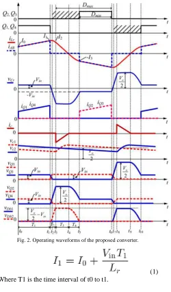
The steady-state operating waveforms are shown in Fig. 2 and detailed operation modes of the proposed converter are shown in Fig. 3. For the proposed converter, Q2 and Q3 are tuned on and off simultaneously; Q1 and Q4 are tuned on and off simultaneously. In order to simplify the analysis of the converter, the following assumptions are made:
1) all switches, diodes, inductor, and capacitor are ideal components;
2) output filter capacitors C1 and C2 are equal and large enough so that the output voltage Vo is considered constant in a switching period Ts.
Fig. 2. Operating waveforms of the proposed converter.
Available online:
https://edupediapublications.org/journals/index.php/IJR/
P a g e | 808Fig. 3. Equivalent circuits of each operation stages. (a) [t0 , t1]. (b) [t1 , t3]. (c) [t3 , t4]. (d) [t4 , t5]. (e) [t5 , t6]. (f) [t6 , t8]. (g) [t8 , t9]. (h) [t9 ,
t10].
In this mode, the energy delivered from Vin to Lr is
(2)
B. Mode 2 [t1, t3] [See Fig. 3(b)]
At t1, Q1 and Q4 are turned off and after that Lr resonates with Cr, vC r decreases from Vin, and iLr increases from I1 in resonant form. Taking into account the parasitic output
Fig. 4. Further equivalent circuits of Mode 2. (a) [t1 , t2]. (b) [t2 , t3]. Capacitors of Q1 through Q4 and junction capacitor of Db2, the equivalent circuit of the converter after t1 is shown in Fig. 4(a), in which CDb2, CQ1, and CQ4 are charged, CQ2 and CQ3 are discharged. In order to realize zero-voltage switching (ZVS) for Q2 and Q3, an additional capacitor, whose magnitude is about ten times with respect to CQ2, is connected in parallel with Db2. Hence, the voltage across Db2 is considered unchanged during the charging/discharging process and Db2 is equivalent to be shorted. Due to Cr is much larger than the parasitic capacitances, the voltages across Q1 and Q4 increase slowly.
Available online:
https://edupediapublications.org/journals/index.php/IJR/
P a g e | 809(6) Where ωr = 1√LrCr , Zr = Lr/Cr , and T2 is the time interval of t1 to t3.
C. Mode 3 [t3, t4] [See Fig.3(c)]
At t3, vC r = −Vo/2, DR1 conducts naturally, C1 is chargedby iLr through DR1, vC r keeps unchanged, and iLr decreaseslinearly. At t4, iLr = 0. The time interval of t3 to t4 is
(7) The energy delivered to load side in this mode is
(8) The energy consumed by the load in half-switching period is
(9)
Assuming 100% conversion efficiency of the converter andaccording to the energy conversation rule, in half-switchingperiod
(10) Combining (7), (8), (9), and (10), we have
(11)
no reverse recovery. After t4, Lr resonates with Cr, Cr is discharged through Lr, vCr increases from −Vo/2 in positive direction, and iLr increasesfrom zero in negative direction. Meanwhile, the voltage across Q4 declines from Vo/2. At t5, vC r = −Vin, and iLr = −I3. In this mode, the whole energy stored in the LC resonant tank isunchanged, i.e.,where T4 is the time interval of t4 to t5.
(13) We have
(14)
(15)
(16)
(17) E. Mode 5 [t5, t6] [See Fig. 3(e)]
If Q2 and Q3 are turned on before t5, then after t5, Lr ischarged by Vin through Q2 and Q3, iLr increases in negativedirection, and the mode is similar to Mode 1.If Q2 and Q3 are not turned on before t5, then after t5, Lr will resonate with Cr , the voltage of node A vA will increasefrom zero and the voltage of node B vB will decay from Vin;zero-voltage condition will be lost if Q2 and Q3 are turned onat the moment. Therefore, Q2 and Q3 must be turned on beforet5 to reduce switching loss.The operation modes during [t6, t10] are similar to Modes2–4, and the detailed equivalent circuits are shown in Fig. 3(f)–(h). During [t6, t10], Q2 and Q3 are turned off at almost zerovoltage, Q1 and Q4 are turned on with ZVS, and DR2 is turnedoff with ZCS.
Available online:
https://edupediapublications.org/journals/index.php/IJR/
P a g e | 810Fig.5.Simulink block diagram under 5MW load condition.
Fig.6.Simulation waveform of the switching pulses (Q1, Q2, Q3 and Q4) for 5MW.
Fig.7.Simulation waveform of the switch voltages (VQ1 and VQ2) for 5MW.
Fig.8.Simulation waveform of the output filter Capacitor Voltages (VC1 and VC2).
Fig.9. simulation waveform of resonant inductor current iLr, capacitor voltage and capacitor Current for 5MW.
Fig.10.Simulation waveform of the input blocking diodes Voltages (VDb1 and VDb2) for 5MW.
Fig.11.Simulation waveform of the switching pulses (Q1, Q2, Q3 and Q4) for 1MW.
Available online:
https://edupediapublications.org/journals/index.php/IJR/
P a g e | 811Fig.13.Simulation waveform of the output filter Capacitor Voltages (VC1 and VC2).
Fig.14. simulation waveform of resonant inductor current iLr, capacitor voltage and capacitor Current for 1MW.
Fig.15.Simulation waveform of the input blocking diodes Voltages (VDb1 and VDb2) for 1MW.
Fig.16. Simulink block diagram for input voltage step.
Fig.17.Input Voltage.
Fig.18.Output Voltage.
Available online:
https://edupediapublications.org/journals/index.php/IJR/
P a g e | 812Fig.20.Simulink block diagram for step load.
Fig.21.Input Voltage.
Fig.22.Output Voltage.
Fig.23. Simulation waveform of resonant inductor current iLr.
Fig.24.Simulink block diagram for PV cell fed Step-up Resonant Converter fed induction motor.
Available online:
https://edupediapublications.org/journals/index.php/IJR/
P a g e | 813Fig.26.simulation results for stator current, speed and electromagnetic torque.
The simulink model for PV fed induction motor is shown in fig .24. The output voltage of resonant converter is given to inverter and the inverted AC supply is fed to induction motor. The AC voltage waveform is shown in fig.25. And the performance characteristics of induction motor like stator current, speed and torque are shown in fig.26.
IV.CONCLUSIONS
A new topology was proposed to improve the resonant converter with the following main characteristics: high boost voltage inversion ability, continuous input current, and resonance suppression at startup. For the same transformer turn ratio and input and output voltage, the improved inverter has a higher modulation index with reduced voltage stress on the dc link, lower current stress flow to the transformer windings and diode, and lower input current ripple. The converter utilizes the resonant inductor to deliver power by charging from the input and discharging at the output. The resonant capacitor is employed to achieve zero-voltage turn-on and turn-off for the active switches and ZCS for the rectifier diodes. This type of impedance network can be used for high step-up inversion ability, and continuous input current. The improved inverter is applicable to fuel cells or photovoltaic applications where a low input voltage must be inverted to a high ac output voltage. It can be further investigated to obtain the output with much reduced current ripples and more voltage gain. In this paper, the converter was designed to drive a three phase induction motor directly from PV solar energy and was conceived to be a commercially viable high efficiency, and high robustness.
REFERENCES
[1].Wu Chen, Member, IEEE, Xiaogang Wu, Liangzhong Yao, Senior Member, IEEE, Wei Jiang, Member, IEEE, and Renjie Hu”A Step-up Resonant Converter for Grid-Connected Renewable Energy
Del., vol. 28, no. 1, pp. 1356–1363, Jul. 2013.
[6] C. Meyer, “Key components for future offshore DC grids,” Ph.D. dissertation, RWTH Aachen Univ., Aachen, Germany, pp. 9–12, 2007. [7] W. Chen, A. Huang, S. Lukic, J. Svensson, J. Li, and Z. Wang, “A comparison of medium voltage high power DC/DC converters with high step-up conversion ratio for offshore wind energy systems,” in Proc. IEEE Energy Convers. Congr. Expo., 2011, pp. 584–589.
[8] L. Max, “Design and control of a DC collection grid for a wind farm,” Ph.D. dissertation, Chalmers Univ. Technol., Goteborg, Sweden, pp. 15– ¨30, 2009.
[9] Y. Zhou, D. Macpherson, W. Blewitt, and D. Jovcic, “Comparison of DCDC converter topologies for offshore wind-farm application,” in Proc. Int. Conf. Power Electron. Mach. Drives, 2012, pp. 1–6.
[10] S. Fan, W. Ma, T. C. Lim, and B. W. Williams, “Design and control of a wind energy conversion system based on a resonant dc/dc converter,” IET Renew. Power Gener., vol. 7, no. 3, pp. 265–274, 2013. [11] F. Deng and Z. Chen, “Control of improved full-bridge three-level DC/DC converter for wind turbines in a DC grid,” IEEE Trans. Power Electron., vol. 28, no. 1, pp. 314–324, Jan. 2013.
[12] C. Meyer, M. Hoing, A. Peterson, and R. W. De Doncker, “Control and ¨ design of DC grids for offshore wind farms,” IEEE Trans. Ind. Appl., vol. 43, no. 6, pp. 1475–1482, Nov./Dec. 2007.
![Fig. 4. Further equivalent circuits of Mode 2. (a) [t1 , t2]. (b) [t2 , t3]. Capacitors of Q1 through Q4 and junction capacitor of Db2, the equivalent circuit of the converter after t1 is shown in Fig](https://thumb-us.123doks.com/thumbv2/123dok_us/7757605.1272585/3.612.64.284.101.566/equivalent-circuits-capacitors-junction-capacitor-equivalent-circuit-converter.webp)

