Looting the LUTs : FPGA Optimization of AES
and AES-like Ciphers for Authenticated
Encryption
Mustafa Khairallah1, Anupam Chattopadhyay1,2, and Thomas Peyrin1,2 1
School of Physical and Mathematical Sciences Nanyang Technological University, Singapore
2
School of Computer Science and Engineering Nanyang Technological University, Singapore
[email protected],[email protected],[email protected]
Abstract. In this paper, we investigate the efficiency of FPGA im-plementations of AES and AES-like ciphers, specially in the context of authenticated encryption. We consider the encryption/decryption and the authentication/verification structures of OCB-like modes (like OTR
or SCT modes). Their main advantage is that they are fully parallelis-able. While this feature has already been used to increase the through-put/performance of hardware implementations, it is usually overlooked while comparing different ciphers. We show how to use it with zero area overhead, leading to a very significant efficiency gain. Additionally, we show that using FPGA technology mapping instead of logic optimization, the area of both the linear and non linear parts of the round function of severalAES-like primitives can be reduced, without affecting the run-time performance. We provide the implementation results of two multi-stream implementations of both theLEDandAESblock ciphers. TheAES imple-mentation in this paper achieves an efficiency of 38 Mbps/slice, which is the most efficient implementation in literature, to the best of our knowl-edge. For LED, achieves 2.5 Mbps/slice on Spartan 3 FPGA, which is 2.57x better than the previous implementation. Besides, we use our new techniques to optimize the FPGA implementation of the CAESAR can-didateDeoxys-Iin both the encryption only and encryption/decryption settings. Finally, we show that the efficiency gains of the proposed tech-niques extend to other technologies, such as ASIC, as well.
Keywords: AES, FPGA, Authenticated Encryption, Logic Optimization,
Tech-nology Mapping,Deoxys,LED
1
Introduction
candidates for round 3 of the CAESAR competition [1]. This competition signi-fies the current need for practical, secure and efficient AEAD schemes. An AEAD scheme typically consists of two routines. The first one is encryptionEK(AD, M) which takes as input a shared keyK, public associated data ADand the mes-sage to be encrypted M and returns a tagged ciphertextC. The second one is decryption/verification DK(AD, C), which either returns an invalid symbol ⊥ if the received ciphertext, associated data and the authentication data do not match, or the decrypted messageM, otherwise.
An important aspect of the study of AEAD schemes is the evaluation of their hardware performance, which clearly needs more efforts. So far, nearly all candi-dates have been supported with a basic hardware implementation [2]. However, the implementations are done on various platforms, for different interfaces and thus, a comprehensive evaluation is still missing. Furthermore, several designs have unique advantages to offer in some platforms, e.g., Field Programmable Gate Array (FPGA), which is not fully exploited. This is one of the prime mo-tivations for this manuscript.
In the survey presented in [3], the authors classified the round 2 candidates of the CAESAR competition into five families according to their base constructions: block cipher-based, stream cipher-based, key-less permutations, hash-function-based and dedicated schemes. In this paper, we focus on the block cipher-hash-function-based family. Specifically, we focus on optimizations for algorithms that allow block-level parallelism while using the underlying block cipher, such as the Offset Code Book mode (OCB) [4–6], the Synthetic Counter-in-Tweak mode (SCT) [7] and the Offset Two-Round mode (OTR) [8].
All the available hardware implementations of the CAESAR competition candidates on the ATHENa hardware evaluation website [2] are fully sequential implementations, i.e. to start processing a new block, all the previous blocks have to be finished. These implementations do not take full advantage of the specific characteristics of the schemes based on the aforementioned modes.
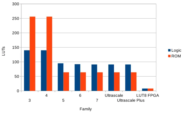
Generally, circuit optimization consists of two phases: logic synthesis and technology mapping. For certain target technologies, such as FPGA, logically optimized circuits do not provide the optimal mapping to the underlying technol-ogy, leaving behind a lot of under-utilized hardware resources. This phenomenon is obvious in the AESSbox circuits proposed by Boyar [9, 10], which are logical optimizations of the circuit proposed by Canright [11]. These circuits are much smaller than the straight-forward ROM-based Sbox in terms of gate count and circuit depth. These two features make them the natural choice for low area Application-Specific Integrated Circuits (ASIC) implementations ofAES. Inter-estingly, on the other hand, practical results show that one can achieve a smaller area on FPGA by using the ROM approach [12]. By analyzing this result, it appears that due to the specific details of these circuits [9–11], it is hard to map them efficiently to look-up tables (LUTs) that the FPGA is constructed from, leading to a lot of under-utilized/unusable logic gates inside the FPGA.
Fig. 1: Evolution of theAESSbox/ISbox area vs. Xilinx FPGA families
is compared with the implementation of Boyar’s shared encryption/decryption Sbox [9]. These results are plotted against the technology evolution of Xilinx FPGAs as an example. Analysing the chart, it is clear that after the intro-duction of the Virtex 5 family, logic optimization of the Sbox stopped being beneficial. The reason for that was the introduction of the 6-input LUTs, which enabled implementing an 8-to-1 look-up table using only four 6-input LUTs and three dedicated multiplexers, or five 6-input LUTs. In other words, the ROM-based Sbox has become both faster and smaller than the logic-ROM-based Sbox, even when both encryption and decryption are implemented using a shared data path. While the technology seems to be saturated around the 6-input LUT structure, a hypothetical family has been added to the chart assuming 8-input LUT struc-ture, showing that such a family will make the cost of both logic-based and ROM-based implementations exactly the same (8 LUTs). While these results may seem specific to Xilinx FPGAs, other vendors, e.g. Altera, also use 6-input LUTs as their building blocks and will follow the same trend. Besides, the FPGA industry seems to be saturated around this building block and we believe that the same trend will follow for the upcoming years.
Our Contributions. In this article, we propose new improvements for FPGA implementations of AEAD schemes based onAES-like primitive. These improve-ments are twofold.
Firstly, we provide a new efficient hardware architecture forOCB-like AEAD modes (Section 2). The architecture uses a generic multi-streamAES-like cipher, such asAESorDeoxys-BC(the tweakable block cipher used in CAESAR compe-tition candidate Deoxys[13]) as an underlying primitive. This architecture can be easily modified to support theOTRorSCTAEAD modes for example.
Secondly, we improve the implementation efficiency of several AES-like ci-phers, such as AES, LED and Deoxys-BC. In particular, the problem of FPGA mapping and under-utilized hardware discussed earlier is studied in details for two applications (Section 3):
– we show how to design low-area logic primitives optimized for FPGA LUTs instead of the number of logic gates (Section 3.2).
– we explain how to select the locations of pipelining registers to accommodate as many independent streams as possible without any additional area cost compared to the single stream architecture (Section 3.3).
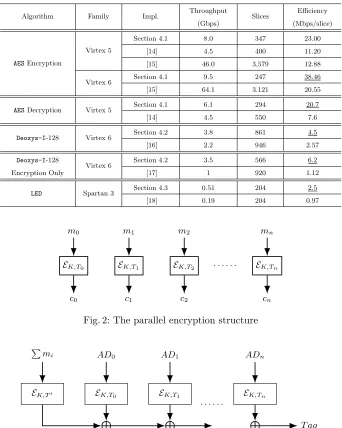
Eventually, as practical results, following these implementation strategies we obtained very efficientLEDand AESimplementations (Section 4). For example, our AES implementation achieves an efficiency of 38 Mbps/slice, which is the most efficient AES FPGA implementation in the literature to the best of our knowledge. We also applied our techniques to Deoxys, and we obtained the current best Deoxys-I FPGA implementation, improving their efficiency by a factor∼1.7 with almost the same area. Table 1 shows a summary of our results compared to state of the art implementations.
2
OCB
Multi-stream Architecture
2.1 OCB Mode Description
Notation. mi is theithplaintext message block. ci is theithciphertext block.
ADi is theith AD block. Ti is the tweak value related to the ith block of the message or AD.Kis the shared secret key.EK,Ti is the bock cipher used by the AEAD algorithm.P
mi is the XOR checksum of the message.
This section includes a simplified description of theOCBmode. An interested reader may refer to [4] for a full description. TheOCBAEAD mode consists of two parts, shown in Figures 2 and 3. In the original proposal [4–6], first the associated data is processed using the PMAC [19] structure shown in Figure 3. Second, the message is encrypted using the structure in Figure 2, computing the message checksum in parallel. Finally, the message checksum in encrypted and XOR-ed to the associated data tag to produce the final tag. These two structures, with minor changes, appear also in other encryption modes, such as OTR, SCT, CTR
Table 1: Summary of our results compared to the state-of-the-art implementa-tions
Algorithm Family Impl. Throughput Slices Efficiency
(Gbps) (Mbps/slice)
AESEncryption
Virtex 5
Section 4.1 8.0 347 23.00
[14] 4.5 400 11.20
[15] 46.0 3,579 12.88
Virtex 6 Section 4.1 9.5 247 38.46
[15] 64.1 3.121 20.55
AESDecryption Virtex 5 Section 4.1 6.1 294 20.7
[14] 4.5 550 7.6
Deoxys-I-128 Virtex 6 Section 4.2 3.8 861 4.5
[16] 2.2 946 2.57
Deoxys-I-128
Virtex 6 Section 4.2 3.5 566 6.2
Encryption Only [17] 1 920 1.12
LED Spartan 3 Section 4.3 0.51 204 2.5
[18] 0.19 204 0.97
EK,T0 m0
c0
EK,T1 m1
c1
EK,T2 m2
c2
· · · EK,Tn
mn
cn
Fig. 2: The parallel encryption structure
ADn
EK,Tn
T ag · · · ·
AD1
EK,T1 AD0
EK,T0 P
mi
EK,T0
Fig. 3: The encrypt-then-xor construction
the ATHENa website [2], the order can be reversed. This enables one to use the same storage for both the checksum and tag computation.
2. In Figure 2 the computations are completely independent, while in Figure 3, there is an output dependency between different blocks. Since there is no input dependency, both the structures are fully parallelisable. Additionally, a small temporal shift saves the temporary storage needed. For example, the first block starts at time t = 0 and the second block starts at t =∆t. At
t = T the first block is finished and stored in the tag storage. Finally, at timet=T+∆tthe second block is finished and XOR-ed with tag, in-place.
2.2 Related Work
The Cryptographic Engineering Research Group (CERG) at George Mason Uni-versity (GMU), USA, runs and maintains the online platform ATHENa [16] aimed at fair, comprehensive, and automated evaluation of hardware crypto-graphic cores targeting FPGAs, All Programmable Systems on Chip, and ASICs. One of their on-going projects is the comparison of FPGA implementations of the CAESAR competition candidates. They have also provided high-speed round-based implementations of round 2 candidates. Among these candidates, several useOCB-like modes:OCBv1.1[20] andAES-OTRv3.1 [21] (which useAESas under-lying cipher), and Deoxys-I v1.41[13] (which uses an AES-like tweakable block cipher Deoxys-BC). Deoxys-BC uses the same data path as AES but defines a new tweak/key-schedule that requires a smaller number of gates to evaluate when compared to AES (but with an additional 128-bit tweak input). It also requires a higher number of rounds compared toAES.
2.3 Proposed Architecture
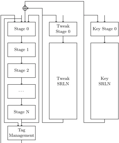
The proposed high level architecture is shown in Figure 4. For simplicity, only the encryption data path is drawn. However, a similar data path for decryption can also be included. The architecture consists of a single round of the under-lying block cipher, which is divided into N stages, each stage takes one cycle to be processed. If the block cipher requires r rounds, the architecture loads and processesN blocks, everyr·N rounds, which leads an average latency ofr
cycles, equivalent to a simple single round implementation. The selection ofN
depends on several considerations:
Stage 0
Stage 1
Stage 2
· · ·
Stage N
Tag Management
Tweak Stage 0
Tweak SRLN
Key Stage 0
Key SRLN
Fig. 4: Multi-stream OCB Hardware Architecture
1. This architecture is intended for high speed over long messages. It is notice-able that any number of blocks less thanNrequires the time to be encrypted. Consequently, a very largeN leads to a huge overhead for short messages or for messages whose block length is not divisible byN.
3. The pipeline registers can add a huge overhead over the simple round im-plementation. Therefore, in Section 3.3 we describe a technique to select the optimal locations of the pipeline registers in the FPGA implementation. From these three considerations, we concluded that the optimal value forN
is between 2 and 4, neglecting the control overhead. This leads to a speed-up be-tween 2x and 4x. Additionally, for applications that require ultra high speed over very long messages, e.g. disk encryption, high speed multimedia interfaces, etc., and do not care about the area, the same architecture can be unrolled into a fully pipelined implementation. This can lead to a huge increase of the throughput. Specifically, the single round multi-stream architecture requires aboutr·N· dB
Ne cycles to compute B blocks. On the other hand, a fully unrolled architecture has an initial latency of r·N and a new block is generated every cycle, lead-ing to a total number of cycles of r·N+B−1. The speed up over the round implementation is given by
G= r·B
r·N+B−1
and for very long messages, the unrolled architecture has a speed up ofrtimes. Since the area increases less than r times (only the round part is replicated while the tag and control part almost have the same area), the efficiency remains unchanged. In Section 4.1 we show that anAESround can be implemented with a clock frequency greater than 700 MHz on FPGA, with almost the same number of slices/LUTs. Therefore, we estimate that this variant can be suitable for applications that require very high speed authenticated encryption.
3
Multi-Stream
AES
-like Ciphers
3.1 AES Data Path State-of-the-Art FPGA Implementations
AES [23] is a 128-bit block cipher, standardized in 2001 by NIST. It is based on the Substitution-Permutation Network (SPN). The internal state of the ci-pher can be viewed as a 4×4 matrix of bytes. It consists of 10 SPN rounds. Each round includes a SubBytes operation for the non-linear part,ShiftRows
andMixColumns for the linear permutation andAddRoundKeyfor key addition.
SubBytes consists of 16 independent 8-bit Sboxes, ShiftRowsshifts the bytes in each row, independently, and MixColumns applies a diffusion matrix to each column, independently. All byte operations are done in GF(28).
implementations. In [14], the authors proposed theAESdata path shown in Fig-ure 5. Each box in FigFig-ure 5 represents a pipeline stage, and it can be noticed that the selection of the pipeline stages is based on the functionality of each stage, which leads to two very fast stages in the beginning, then two slow stages after-wards. This limits the maximum possible frequency. In the next sections, we will show why this architecture might not be optimal and describe a new four-stream data path designed for FPGA to achieve higher performance efficiency.
Input Selection
Add Key
Sbox
MixColumns
Fig. 5: TheAESencryption data path from [14]
3.2 LUT-based Optimization of Linear Transformations
Notation. a, b, canddare the four bytes that compose one column of theAES
state.aiis theithbit ofa, wherea0is the least significant bit. Upper-case letters
A, B, C, D, E, F are the hexadecimal representations of the decimal values 10, 11, 12, 13, 14 and 15, respectively.·and⊕are multiplication and addition over GF(28).
TheAES MixColumns circuit is a matrix multiplication operation of theAES
state byte matrix by a constant matrixM given by
2 3 1 1 1 2 3 1 1 1 2 3 3 1 1 2
which is a circulant MDS matrix. ForAES128-bit architectures, theMixColumns
operation can be viewed as 16 dot-products of the vector 2 3 1 1
Specifically, only 108 XOR gates are required for implementing the 32-bit map-ping [26]. However, as discussed earlier, since modern FPGAs use big 6/5 input LUTs to implement logic circuits, having a lot of small shared 2/3-input gates is not the most efficient solution. Synthesizing the circuit used in [26] or [27] for Virtex-6 FPGA requires 41 LUTs for low area and 44 LUTs for high speed. On the other hand, the dot-product view is given by
p= 2·a⊕3·b⊕c⊕d
which can be decomposed into
a6a5a4a3a2a1a0 0
0 0 0 a7a7 0 a7a7
b6 b5 b4 b3 b2 b1 b0 0
0 0 0 b7 b7 0 b7 b7
b7 b6 b5 b4 b3 b2 b1 b0
c7 c6 c5 c4 c3 c2 c1 c0
d7d6d5d4d3d2d1d0
(1)
where the elements of each column represent the inputs of one output function. From this perspective, it can be seen that 5 outputs can be implemented using one 5-input LUT, while 3 outputs can be implemented using 7-input LUT, which can be implemented using two 6-input LUTs. That sums to a total of 11 LUTs per output coefficient, 44 LUTs per output column. This shows that logic opti-mization does not offer much gain over the straightforward implementation of the transformation. Besides, a deeper look at the view given by the decomposition in (1) shows that the three outputs that need 7-input LUTs share two inputs bits, namely a7&b7. Decomposition (1) can be written as decomposition (2),
wherex=a7⊕b7. This decomposition can be implemented using eight 6-input
LUTs and one 2-input LUT, a total of 9 LUTs per output coefficient, 36 LUTs per output column (which is smaller than the best-reported implementations) or 1.125 LUTs per output bit. It is worth mentioning that this number is near-optimal for any linear transformation over 32 bits, as the near-optimal number is 1 LUT/bit, which corresponds to transformation where each output bit depends on n bits, where 2≤n ≤6 (the case where n= 1 corresponds to an identity function and can be neglected, w.l.o.g.)3.
3 In fact, each 6:1 LUT can be implemented as a 5:2 LUT with shared inputs. Using
a6a5a4a3a2a1a0a7
b6 b5 b4 b3 b2 b1 b0 b7
0 0 0 x x 0 x 0
b7 b6 b5 b4 b3 b2 b1 b0
c7 c6 c5 c4 c3 c2 c1 c0
d7d6d5d4d3d2d1d0
(2)
The optimization of the AES inverseMixColumns circuit is less straightfor-ward, as M−1 includes larger coefficients.M−1 is given by
E B D 9 9 E B D D 9 E B B D 9 E
A lot of work has been done on how to reuse the same circuit from M
to implement M−1 with minimal overhead. This is done by using any of the following relations M−1 = M3, M−1 = M ·N or M−1 = M ⊕K, where N
andK are matrices with low coefficients. In that direction, the circuit given by decomposition (2) will also be the smallest and the same reasoning can be used to achieve small area for bothK andN. However, this approach is most useful for low area serial implementations with shared encryption/decryption data path. They do not achieve the best results for high speed round implementations with dedicated decryption data path. For example, usingM−1=M3 requires 3.375
LUTs/bit and produces a large-depth circuit (low performance), while using
M−1=M ⊕K is even larger. The most promising approach is M−1 =M·N
which requires 288 LUTs/block, corresponding to 2.25 LUTs/bit, which is still far from optimal. On the other hand, the straightforward implementation of
M−1 leads to output functions that include 19 input bits, which can lead to
very low performance. Here, we give a circuit that requires 60 LUTs per output column, corresponding to 1.875 LUTs/bit. First, we use the same dot product view mentioned earlier, which is given by equation (3).
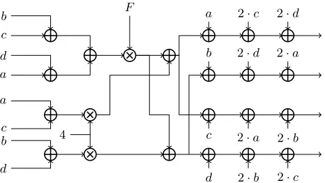
p0=E·a⊕B·b⊕D·c⊕9·d=F·(a⊕b⊕c⊕d)⊕(a⊕4·b⊕2·c⊕4·d⊕2·d) (3) Second, two observations are made
1. F·(a⊕b⊕c⊕d) is constant across any output column.
2. 4·(a⊕c) is shared by two output coefficients. The same is valid for 4·(b⊕d). Using these two observations, a circuit that requires only 60 LUTs per output column can be implemented. The circuit diagram is given in Figure 6. This is 17% smaller than the best reported implementation. Given that MixColumns
a c b
d
F
a
c b
d
4
a 2·c 2·d
b 2·d 2·a
c 2·a 2·b
d 2·b 2·c
Fig. 6: FPGA-friendly inverseMixColumns circuit
3.3 Zero Area Overhead Pipelining
Pipelining has been used by hardware designers/architects as a tool to increase throughput/run-time performance for a long time. However, a fully pipelined block cipher implementations can be costly, due to the large area requirements. A more realistic approach is to use multi-stream implementations. These imple-mentations start from a sequential implementation that processes one block in
Ccycles, and divides it intoN pipeline stages. This leads to computingxblocks inN·Ccycles, wherex∈ {1,2, ..., N}.xdepends on the number of independent block streams the user can leverage. However, this is a double-edged weapon, due to the following reasons:
1. The time required to process one block in a sequential implementation is
∼C·T, whereT is the critical path delay of the implementation. If theN
pipeline stages divide the critical path evenly into segments of NT delay, the time required to processN blocks becomesT+t, wheretis a small overhead, leading to ∼ Nx speed-up. Unfortunately, the critical path is usually not evenly divided, leading to a sub-optimal speed-up (< N).
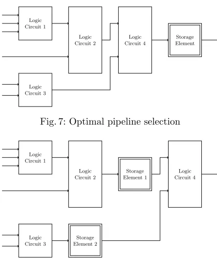
2. Modern FPGA families consist of a basic building block called LUT6, which is a 6-input single-output look-up table. Additionally, each unit of this build-ing block has an associated Flip-Flop, which the designer/synthesis tool can choose to either use it or not. In Figure 7, we show the optimal utilization of a LUT6 unit in a pipelined architecture, where it is used to implement a 6-input circuit followed by storing the output. On the other hand, in Fig-ure 8, a poor selection of the location of pipeline stage is in-place, leading to the utilization of 3 look-up tables, instead of 1 in the case of Figure 7. In other words, the poor choice of where to place the pipeline registers leads to a significant increase in area.
Logic Circuit 1
Logic Circuit 2
Logic Circuit 3
Logic Circuit 4
Storage Element
Fig. 7: Optimal pipeline selection
Logic Circuit 1
Logic Circuit 2
Storage Element 1
Logic Circuit 3
Storage Element 2
Logic Circuit 4
Fig. 8: Sub-optimal pipeline selection
the pipeline stages based on the logical functions, e.g. Sbox,MixColumns, input selection, etc. In our work, we follow a different approach. First, we synthesize a single stream sequential implementation of the required block cipher. Second, we study the output layout to to determine the precise distribution of pipeline stages without affecting the structure of the utilized LUTs.4.
4
Implementations and Results
4.1 Two-Stream and Four-Stream AESImplementations
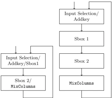
Using the techniques described in Sections 3.2 and 3.3, we have implemented two multi-stream AESdata path (two and four streams), shown in Figure 9. In addition to the use of the low area MixColumns circuit and ROM-based Sbox, the locations of the pipelining registers have been selected specifically to ensure as efficient LUT utilization as possible. In other words, both the two-stream and four-stream implementations use the same number of logical LUTs (944 LUTs, without key scheduling), out of which 95% (896 LUTs) are 6-input LUTs. The
4
Input Selection/ Addkey/Sbox1
Sbox 2/
MixColumns
Input Selection/ Addkey
Sbox 1
Sbox 2
MixColumns
Fig. 9: Two/Four-StreamAESround data path implementation
results are given in Table 2. The comparison is restricted to full-width imple-mentations that do not utilize any BRAMs. For that reason, the implementation in [28] is not included. While it has a very high efficiency (yet smaller than ours,
∼30 Mbps/slice), this number is biased due to the use of BRAMs to reduce the number of slices. It can be observed that our data path, with only two-streams, outperforms the data path from [14] (with four streams) in terms of both effi-ciency and area and reaches the same throughput. This result is achieved due to more than one factor:
1. The critical path in the implementation from [14] consists of three levels of logic inside the Sbox used (one LUT6 followed by MUX7 and MUX8). In our design, the critical path also consists of three levels of logic (Sbox part 2 (LUT6) and theMixColumns circuit proposed in Section 3.2 (LUT3 + LUT6)).
2. TheMixColumns circuit used is smaller.
3. The first two pipeline stages in Figure 5 necessitate the use of 256 LUTs. The two stages altogether can be viewed as a 6-input function, which can be easily merged into a single stage of 128 LUTs (of type LUT6).
It is shown that it has a speed-up of around 2x over the similar implementation from [14].
Table 2: Implementation results ofAESon Virtex-5/6 FPGA (encryption only)
Family Implementation Key Number Max. freq Throughput Efficiency
schedule of Slices (MHz) (Gbps) (Mbps/slice)
Virtex 5
Ours/2 streams Offline 347 350 4.5 12.90
Ours/4 streams Offline 347 625 8.0 23.00
[14]/4 streams Offline 400 350 4.5 11.20
[15]/ unrolled Offline 3579 360 46.0 12.88
Virtex 6
Ours/4 streams Offline 347 752 9.6 27.66
Ours/4 streams No 247 752 9.5 38.46
[15]/ unrolled Offline 3121 501 64.1 20.55
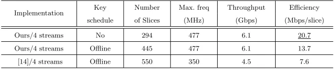
Table 3: Implementation results of AESon Virtex-5 FPGA (decryption only)
Implementation Key Number Max. freq Throughput Efficiency
schedule of Slices (MHz) (Gbps) (Mbps/slice)
Ours/4 streams No 294 477 6.1 20.7
Ours/4 streams Offline 445 477 6.1 13.7
[14]/4 streams Offline 550 350 4.5 7.6
4.2 Round-based Two-Block Deoxys-I-128
As mentioned earlier, the Deoxys-I CAESAR candidate uses an underlying tweakable block cipher called Deoxys-BC. This cipher is similar to AES, with three major differences:
1. It consists of 14 rounds instead of 10.
2. The final round includes a MixColumnsoperation, as opposed toAES. 3. It uses a different key schedule, which is smaller than the AESkey schedule,
but uses an extra public tweak value.
Based on the architecture proposed in Section 2 and the AES data paths proposed in Section 4.1, we have implemented two complete data paths for
key schedule and the tweak schedule. Using the pipeline selection technique, both implementations consume the same area, except for the decryption data path which we implement only for 4 streams. In Table 4, it is shown that the bottleneck of the design, not considering the control overhead, is the decryption data path.
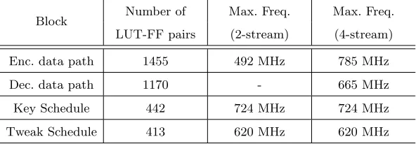
Table 4: Results of the Deoxys-I-128 data path implementation on Virtex-6 FPGA
Block Number of Max. Freq. Max. Freq.
LUT-FF pairs (2-stream) (4-stream)
Enc. data path 1455 492 MHz 785 MHz
Dec. data path 1170 - 665 MHz
Key Schedule 442 724 MHz 724 MHz
Tweak Schedule 413 620 MHz 620 MHz
Based on this datapath, a full implementation of Deoxys-I-128 has been implemented on Xilinx Virtex-6 FPGA (xc6vlx75tff784-3). The overall utiliza-tion is ∼ 3800 LUT-FF pairs and maximum operating frequency is 454 MHz. This 27% performance degradation from the datapath estimated clock frequency comes from two reasons:
1. While the datapath is very fast, there is still optimization required to the control unit to cope with such speed.
2. Although we choose a small FPGA from the Virtex 6 family, the design is still small compared to the FPGA size, which leads to it becoming I/O dominated. leading to a lot of wiring delays related to the I/O pins. This will not be applicable if the design is used as a part of a larger on-chip system.
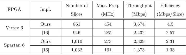
Table 5: Post-layout results of theDeoxys-I-128 implementation on FPGA
FPGA Impl. Number of Max. Freq. Throughput Efficiency
Slices (MHz) (Mbps) (Mbps/Slice)
Virtex 6 Ours 861 454 3,874 4.5
[16] 946 285 2,432 2.57
Spartan 6 Ours 1,010 273 2,329 2.31
[16] 1,032 161 1,373 1.33
Table 6: Post-layout results of theDeoxys-I-128 encryption only implementation on Virtex 6 FPGA
Impl. Number of Max. Freq. Throughput Efficiency
Slices (MHz) (Mbps) (Mbps/Slice)
Ours 566 416 3,549 6.2
[17] 920 161 1.030 1.12
Relevance to the CAESAR Competition The goal of this section is not
to show that Deoxys-I is faster than other CAESAR candidates. The goal is to show that parallelism can actually increase the efficiency of parallelisable ciphers by significant factors. Since we are comparing two different architectures and implementations of the same cipher, it makes more sense to focus the comparison on the cipher itself. While the API provides a fair methodology for comparing different ciphers, it can hide the potential of enhancement for a certain cipher. This is exactly true for FPGA in our case, as a custom control unit that is both compliant with the CAESAR API and the 4-stream architecture has to be designed. This leads to 50% decrease in the performance of the proposed architecture during the CAESAR Competition Round 3 benchmarking stage. We emphasize that this is not the goal of the proposed architecture, as in real-life applications faster APIs can be designed, such as the one we used in the previous comparison.
Extending the results to other technologies (ASIC) Since it can be
Table 7. We are currently in the process of preparing the HDL code to be pro-vided publicly soon so that other researchers can verify our results.
Table 7: Synthesis results of the Deoxys-I-128 implementation using TSMC 65nm technology
Impl. Area Max. Freq. Throughput Efficiency
(KGE) (MHz) (Mbps) (Mbps/KGE)
Ours 59.53 847 7,227 121.40
[16] 53.37 549 4,684 87.76
4.3 Three-Stream LEDImplementation
Input Selection/ Addkey
Sbox
MixColumns
Fig. 10: Three-Stream (χ4)LED-64 round implementation
LED [29] is a 64-bit block cipher based on anAES-like SPN. Its state is a 4×4 matrix of 4-bit nibbles. In this paper we focus on the 64-bit key versionLED-64. However, the same results can extend to the other variants of LED, since the only difference is the key scheduling part, which can be easily adjusted for this architecture. The (χ4) round implementation from [18], Section 3.1, has been
Table 8: Results of the three-stream LED-64 implementation compared to the single stream counterpart on Spartan 3 FPGA.
Implementation Number Number Max. freq Throughput Efficiency of Slices of FFs (MHz) (Mbps) (Mbps/slice)
[18]/1 stream 204 74 98.7 197.35 0.97
Ours/3 streams 204 202 257 514 2.5
Acknowledgments
The authors would like to thank the anonymous referees for their helpful com-ments. This work is partly supported by the Singapore National Research Foun-dation Fellowship 2012 (NRF-NRFF2012-06).
References
1. CAESAR Competition: CAESAR submissions.
https://competitions.cr.yp.to/caesar-submissions.html (2016)
2. George Mason University: ATHENa: Automated Tools for Hardware EvaluatioN. https://cryptography.gmu.edu/athena/ (2017)
3. Abed, F., Forler, C., Lucks, S.: General classification of the authenticated encryp-tion schemes for the CAESAR competiencryp-tion. Computer Science Review (2016) 4. Rogaway, P., Bellare, M., Black, J.: OCB: A block-cipher mode of operation for
efficient authenticated encryption. ACM Transactions on Information and System Security (TISSEC)6(3) (2003) 365–403
5. Rogaway, P.: Efficient instantiations of tweakable blockciphers and refinements to modes OCB and PMAC. In: International Conference on the Theory and Appli-cation of Cryptology and Information Security, Springer (2004) 16–31
6. Krovetz, T., Rogaway, P.: The software performance of authenticated-encryption modes. In: International Workshop on Fast Software Encryption, Springer (2011) 306–327
7. Peyrin, T., Seurin, Y.: Counter-in-tweak: authenticated encryption modes for tweakable block ciphers. In: Annual Cryptology Conference. (2016)
8. Minematsu, K.: Parallelizable rate-1 authenticated encryption from pseudorandom functions. In: EUROCRYPT, Springer (2014) 275–292
9. Boyar, J., Peralta, R.: A new combinational logic minimization technique with applications to cryptology. In: International Symposium on Experimental Algo-rithms, Springer (2010) 178–189
10. Boyar, J., Peralta, R.: A small depth-16 circuit for the AES s-box. In: IFIP International Information Security Conference, Springer (2012) 287–298
11. Canright, D.: A very compact s-box for AES. In: International Workshop on Cryptographic Hardware and Embedded Systems, Springer (2005) 441–455 12. Resende, J.C., Chaves, R.: AES Datapaths on FPGAs: A State of the Art Analysis.
13. Jean, J., Nikolic, I., Peyrin, T., Seurin, Y.: Deoxys v1.41. Technical report, Nanyang Technological University, Singapore/ANSSI, Paris, France (2016) 14. Bulens, P., Standaert, F.X., Quisquater, J.J., Pellegrin, P., Rouvroy, G.:
Imple-mentation of the AES-128 on Virtex-5 FPGAs. In: International Conference on Cryptology in Africa, Springer (2008) 16–26
15. Liu, Q., Xu, Z., Yuan, Y.: A 66.1 gbps single-pipeline aes on fpga. In: 2013 International Conference on Field-Programmable Technology (FPT). (Dec 2013) 378–381
16. : Deoxys-I-128 implementation by cerg team.
https://cryptography.gmu.edu/athena/ (2016)
17. Poschmann, A., St¨ottinger, M.: Deoxys-I-128 implementation by poschmann and St¨ottinger. https://cryptography.gmu.edu/athena/ (2016)
18. Anandakumar, N.N., Peyrin, T., Poschmann, A.: A very compact FPGA imple-mentation of LED and PHOTON. In: International Conference in Cryptology in India, Springer (2014) 304–321
19. Black, J., Rogaway, P.: A block-cipher mode of operation for parallelizable message authentication. In: International Conference on the Theory and Applications of Cryptographic Techniques, Springer (2002) 384–397
20. Krovetz, T., Rogaway, P.: Ocb (v1. 1). (2016)
21. Minematsu, K.: AES-OTR v3.1. Technical report, (NEC Corporation, Japan
(2016)
22. Homsirikamol, E., Diehl, W., Ferozpuri, A., Farahmand, F., Yalla, P., Kaps, J.P., Gaj, K.: CAESAR Hardware API. Cryptology ePrint Archive, Report 2016/626 (2016)
23. NIST: National Institute of Standards and Technology: Advanced Encryption Standard AES (2001)
24. El Maraghy, M., Hesham, S., El Ghany, M.A.A.: Real-time efficient fpga im-plementation of aes algorithm. In: SOC Conference (SOCC), 2013 IEEE 26th International, IEEE (2013) 203–208
25. Chaves, R., Kuzmanov, G., Vassiliadis, S., Sousa, L.: Reconfigurable memory based aes co-processor. In: Parallel and Distributed Processing Symposium, 2006. IPDPS 2006. 20th International, IEEE (2006) 8–pp
26. Banik, S., Bogdanov, A., Regazzoni, F.: Atomic-AES v 2.0. Cryptology ePrint Archive, Report 2016/1005 (2016)
27. Ghaznavi, S., Gebotys, C., Elbaz, R.: Efficient technique for the FPGA implemen-tation of the aes mixcolumns transformation. In: Reconfigurable Computing and FPGAs, 2009. ReConFig’09. International Conference on, IEEE (2009) 219–224 28. Resende, J.C., Chaves, R.: Compact dual block aes core on fpga for ccm protocol.
In: Field Programmable Logic and Applications (FPL), 2015 25th International Conference on, IEEE (2015) 1–8
![Fig. 5: The AES encryption data path from [14]](https://thumb-us.123doks.com/thumbv2/123dok_us/7962555.1320815/9.612.266.349.219.369/fig-aes-encryption-data-path.webp)