This thesis covers research based on ab initio calculations (Hartree-Fock combined with
Configuration Interaction) on two materials systems: SiO2 defects in a tetrahedral network
and ZnO defects in a wurtzite crystal.
Owing to its importance in the semiconductor industry, SiO2 has been studied
extensively. Of particular interest here is the oxygen “vacated-site” defect, which has been
studied by the Lucovsky group from XAS data. We start with a SiO2 cluster constructed with
optimized bond lengths, bond angles, and medium-range order. The same geometrical basis
is then applied to the oxygen vacated-site defect structure. General properties of its ground
and excited states within the band gap are revealed.
Wurtsite ZnO is a candidate material for light emission. Dr. Reynolds working in the
Aspnes group has developed a series of processing steps leading to significant p-type
behavior, and has investigated the effect of the different steps using Raman scattering. Here,
the intermediate and final stages of this progression are investigated theoretically. We
explore the relationship between various defect sites and p-type conductivity. The ZnO
defects are studied with a structural model that uses the experimentally determined
parameters. Defect sites related to N doping and single Zn/O vacancies are created and
compared. H atoms are also introduced to mimic conditions that occur in metal-organic
by Kun Wu
A dissertation submitted to the Graduate Faculty of North Carolina State University
in partial fulfillment of the requirements for the degree of
Doctor of Philosophy
Physics
Raleigh, North Carolina
2013
APPROVED BY:
_______________________________ ______________________________
Dr. David Aspnes Dr. Jerry Whitten Chair of Advisory Committee
________________________________ ________________________________
DEDICATION
BIOGRAPHY
Kun Wu was born on Jan. 1st. 1987 in Wan’an, Jiangxi Province, P.R. China. His interest in
Physics started in middle school. Admitted into Shanghai Jiao Tong University in 2004, he
majored in Optics&Physics. After graduation in 2008, he came to North Carolina State
University for the pursuit of a PhD degree in Physics. Starting from 2010, he took the role of
research assistant in Prof. Gerald Lucovsky’s group and focused on calculation and
experiment of SiO2 defect. In 2012, he switched to work for Prof. Dave Aspnes on ZnO
defect sites. He fulfilled the requirements of the Doctor of Philosophy degree in Physics at
ACKNOWLEDGMENTS
I hereby express my gratitude to my committee members, Dr. Dave Aspnes, Dr. Jerry
Whitten, Dr.Gerald Lucovsky and Dr. Mike Whangbo for their generous guidance and
review of this work. I owe special thanks to Dr. Jerry Whitten for his patient guidance on
theoretical calculation that covers all the topics here. And I am grateful that Dr. Lucovsky
and Dr. Aspnes provided me with interesting research topics.
I would like to extend my gratitude to my former and current colleagues, Dr. Brian Papas,
Dr. Jinwoo Kim, Daniel Zeller, Cheng Cheng, and Yinglei Zhang. It is my pleasure to work
with you and support from you also played an important role in my research.
I also thank my numerous friends at NCSU, such as Elliot Gann, Ziran Gu, Donald
Warren, Craig Huffer, David Fallest, Shi Guo, Chengbo Han, Nick Truelove, Eric Raymer,
Austin Reid, Dr. Brandon Lunk, Carlos Ortiz,Keeley Stevens,etc. Our friendship made my
experience here much more enjoyable.
I dedicate this thesis to my parents for the great sacrifice they made for my education and
career. Without their effort, this work would have never been possible. My love would be
TABLE OF CONTENTS
LIST OF TABLES ... viii
LIST OF FIGURES ... ix
Chapter 1 : Introduction of the theory... 1
1.1 Definition of Hamiltonian ... 1
1.2 Hartree-Fock Self-Consistent Field(SCF) Method ... 2
1.3 Orbital Energy-Fock operator ... 5
1.4 Gaussian Type Orbitals ... 5
1.5 Localization ... 6
1.6 Ion calculation ... 6
1.7 Mulliken population analysis. ... 7
1.8 Pseudopotential treatment. ... 9
1.9 Configuration Interaction. ... 10
1.10 Transition dipole ... 11
1.11 Overview of dissertation work ... 11
1.12 References ... 12
Chapter 2 : Background on SiO2 topics. ... 15
2.1 SiO2/Si in the semiconductor industry ... 15
2.2 Research on O-vacancy defects ... 17
2.8 References... 18
Chapter 3 : The SiO2 defect: case study. ... 22
3.1 Structural basis for a-SiO2 . ... 23
3.1.1 Local parameters: bond length and bond angle ... 23
3.1.2 Medium Range Order. ... 24
3.1.3. Band transition. ... 26
3.2 Ground state of the defect site. ... 26
3.3.1 Bonding of a Si atom ... 32
3.3.2 Single “dangling bond” on Si ... 33
3.3.3 Interaction between “dangling bonds”. ... 34
3.3.4 Influence of bond angles. ... 37
3.3.5 Influence of the bulk ... 38
3.4 Summary of the calculation. ... 41
3.5 Comments on the XAS analysis. ... 42
3.6 References... 45
Chapter 4 : The ZnO calculation. ... 89
4.1 Structure and properties. ... 89
4.2 Light Emitting Diodes... 91
4.2.1 General Semicoductor LEDs ... 91
4.2.2 Blue, Violet and UV LEDs. ... 92
4.2.3 p-type ZnO ... 94
4.3 References... 95
Chapter 5 : ZnO defect case study. ... 107
5.1 Model ... 107
5.1.1 Bond length and angle. ... 107
5.1.2 Determining the cluster. ... 108
5.2 Transition from the Vo-NZn to No-VZn and No-VZn-H configurations. ... 111
5.2.1 Vo-NZn to No-VZn transition. ... 112
5.2.2 No-VZn-H configuration. ... 114
5.3. Intrinsic defect sites with H. ... 118
5.3.1. Oxygen vacancy (Vo) with H. ... 118
5.3.2 Zinc vacancy (VZn) with H. ... 121
5.3.3 Interstitial H atoms. ... 122
5.4 Conclusion and comments. ... 125
Chapter 6: Summary and Future Work. ... 154
6.1 Summary. ... 154
6.2 Future Work... 155
APPENDICES ... 156
LIST OF TABLES
Table 4.1: Measured parameters of ZnO wurtzite crystal ... 106
LIST OF FIGURES
Figure 1.1: Scheme of Hartree Fock SCF calculation ... 13
Figure 1.2: Flowchart for combined Hartree Fock SCF-CI method. ... 14
Figure 2.1: Scheme of MOS transistor ... 20
Figure 2.2: Scheme of X-ray interaction with matter ... 21
Figure 3.1: Schematic of two tetrahedrons bonded together, from ref [2]. ... 47
Figure 3.2: Bond length vs. Ground state energy with optimized bond angle... 48
Figure 3.3: Bond angle vs. total energy of the geometry with optimized bond length. ... 49
Figure 3.4: Calculated Si-O-Si bond length, from ref [2]. ... 50
Figure 3.5: Si-O bond lengths of various form of SiO2. ... 51
Figure 3.6: A 3D view of the cluster configuration for silica. ... 52
Figure 3.7: Total energy of lowest singlet and triplet states. ... 53
Figure 3.8: Contour plotof the two molecular orbitals that singlet and triplet lowest states are constructed out of. ... 54
Figure 3.9: Behavior of E(lower curve),E*(upper curve) with respect to Si-Si distance. .. 55
Figure 3.10: Behavior of J(solid line),J**(solid line with dots)and J*(dash line). ... 56
Figure 3.11: Energy of K*(lower curve) and the square root term in Eq.3.7 ... 57
Figure 3.12: E-E0 for the two orbitals for singlet (bottom line on left), triplet (middle line on left) and E0 (top line on left)... 58
Figure 3.13: Energies of the lowest singlet and triplet states for the vacancy (dots) and vacated-site (dash line) geometry.. ... 59
Figure 3.14: Energy diagram from a single Si atom. ... 60
Figure 3.15: Si(OH)4 structure with Td(a) and C3v(b) symmetry.. ... 61
Figure 3.16: Energy diagram of Si(OH)4. ... 62
Figure 3.17: Contour plot of different type of orbitals in Si(OH)4. ... 64
Figure 3.19: Contour plots of the E representation (a and b/top) and A1 representation (c,
bottom) that correspond to the T2 representation from Si 3p under Td. ... 68
Figure 3.20: Excitation from the Si(OH)3 structure. ... 70
Figure 3.21: The Si2(OH)6 structure.. ... 72
Figure 3.22: Evolution of HOMO and Si 4s, 3d virtual orbitals from Si(OH)3 to Si2(OH)6.. 73
Figure 3.23: Excitation from the singlet ground state of the Si2(OH)3 system. ... 74
Figure 3.24: Excitation from the lowest triplet state for the Si2(OH)6 system. ... 76
Figure 3.25: Singlet transition from Si2(OH)6 where the Si dangling bonds form an angle of 148º. ... 77
Figure 3.26: Triplet transition for Si2(OH)6 where the Si dangling bonds form an angle of 148º. ... 78
Figure 3.27: The vacated-site structure viewed from different angles. ... 79
Figure 3.28: Comparison between Si(OH)3 and one-side of the bigger cluster... 80
Figure 3.29: Transition from one-side of the expanded cluster. ... 81
Figure 3.30: Singlet transition from the whole cluster shown in Fig. 3.27... 82
Figure 3.31: Triplet transition from the whole cluster shown in Fig. 3.27. ... 84
Figure 3.32: Singlet transition from the big cluster where the Si dangling bonds forms an angle of 148º. ... 85
Figure 3.33: Triplet transitions from the big cluster where the Si dangling bonds form an angle of 148º. ... 86
Figure 3.34: A typical SiO2 XAS OK edge spectrum of nc (nanocrystalline) -SiO2 formed by remote plasma deposition (RPD) and annealed at 950 °C in Ar for 1 min [7]. ... 87
Figure 3.35: A second-derivative O K pre-edge spectrum of remote plasma deposited SiO2 annealed at 900 °C for 1 min in Ar [7]. ... 88
Figure 4.1: rocksalt(a/left) and zinc blende(b/right) structure model ... 101
Figure 4.2: wurtzite structure model. ... 102
Figure 4.4: Scheme of a Light Emitting Diode ... 104
Figure 4.5: Schematic diagram of a n-ZnO/ p-Al0.12Ga0.88N heterojunction ... 105
Figure 5.1: Definition of parameter b1, b2 and b3. ... 127
Figure 5.2: Side view of the cluster with point charges. ... 128
Figure 5.3: Top down view of the cluster with point charges. ... 129
Figure 5.4: Layer structure of ZnO viewed from different angles. ... 130
Figure 5.5: The final cluster for bulk ZnO. ... 131
Figure 5.6: Fig. 6.6 The initial (Vo-NZn) and final state(VZn-No) of N defect site. ... 132
Figure 5.7: The energy of the entire system with the N atom placed on different locations along the c axis... 133
Figure 5.8: Contour plot of HOMO’s for the system when N is (a/top left ) at an Oxygen site, (b/top right ) in the middle (0Å in Fig 6.7), (c/bottom) at a Zn site. ... 134
Figure 5.9: Energy of the system versus displacement of the N atom perpendicular to the c axis at a Zn site (top) and an O site (bottom). ... 136
Figure 5.10: Evolution of the total energy of the system during optimization. ... 137
Figure 5.11: Evolution of the step size for N, H atom, and N-H distance during optimization. ... 138
Figure 5.12: No-VZn-H confguation with N-H bonding. ... 139
Figure 5.13: Contour plot of the two singly occupied orbitals in the neutral No-VZn-H complex. ... 140
Figure 5.14: The optimized geometry with all orbitals doubly occupied. ... 141
Figure 5.15: Energy curve of H-N bond stretching mode. ... 142
Figure 5.16: Contour plot for the HOMO of VZn site.. ... 143
Figure 5.17: Interaction between the HOMO’s of the Vo site and the H atom. ... 144
Figure 5.18: Energy curves for the A1 and E mode of the Vo-H configuration. ... 145
Figure 5.19: Energy curve of the two Raman modes for the Vo-H+ configuration. ... 146
Figure 5.21: Contour plot of the only singly occupied orbital for the two O-H bonding cases.
... 148
Figure 5.22: Geometry of two H interstitial configurations where H is bonded closely to an O
atom... 149
Figure 5.23: Two H interstitial configurations where H shows little interaction with with the
rest of lattice. ... 150
Chapter 1
: Introduction of the theory.
All the defects reported in the thesis are studied by an ab initio approach. The calculation
is carried out under Dr. Jerry Whitten’s supervision, with the help from Dr. Brian Papas. The
original data are available on sever jwm2/jw3.chem.ncsu.edu. The Introduction provides a
description of general methods, summarized from various lecture notes. Some crucial
technical details are also discussed.
1.1 Definition of Hamiltonian
The method solves for total electron wavefunctions under a static framework of nuclei.
Thus the Hamiltonian of the system only includes the electronic terms. It is written as
∑ ∑ ∑ (1.1)
In the above equation, i and j are indices for electrons and k is for nuclei. is the
Laplacian operator,
(1.2)
which is used to calculate the kinetic energy of the electron i. It is also written as T for
simplicity. ∑ , sometimes written as V, is the nuclear attraction for the single
electron i. 1/rij stands for the repulsion between electrons i and j. To avoid the complication
of constants such as h and e, atomic units (a.u) are adopted. For length, 1 a.u = 1
bohr=a0=0.5292Å. For energy, 1 a.u = 1hartree=e2/a0=27.21eV.
(1.3)
where E is the total energy of the electronic system. In this work, the equation is solved by a
two step process, a Hatree-Fock Self-Consistent Field (SCF) calculation followed by
Configuration Interaction (CI) calculation.
1.2 Hartree-Fock Self-Consistent Field(SCF) Method
Electrons are fermions. The total wavefunction of an electron system is required to be
antisymmetric. To satisfy such a requirement, the SCF method constructs the total
wavefunction as
⁄ (1.4)
where
(1.5)
is a one-electron wavefunction. It consists of a spatial orbital and a spin function ( ⁄ ).
is a set of orthogonal wavefunctions so that
(1.6)
These one-electron wavefunctions are of the general form
∑ (1.7)
where is an orthonormal set of atomic orbitals.
The solution of Eq. (1.6) is guided by the Variational Principle. It requires the
optimization of the cmk’s so that the total energy of the system
is minimized.
It is informative to take closed shell molecules as an example. Spatial orbitals are
occupied by electron pairs with opposite spin. Thus for the set of occupied spatial orbitals
{ }, the overall energy E is written as:
∑ ⟨ | | ⟩ ∑ ∑ ⟨ |
| ⟩
∑ ∑ ⟨ |
| ⟩ (1.9)
where h = T + V. The two terms involving the electron interaction are phrased as coulomb
repulsion (Jij) and exchange interaction (Kij) respectively. So the equation is simplified as
∑ ⟨ ⟩ ∑ (1.10)
This E expression is then optimized by the SCF theory of Roothann [1]. Lagrangian
multipliers are introduced to the expression for E.
Suppose that a change of coefficient Cmk’s generates a new energy E’ as
∑ ⟨ ⟩ (1.11)
To achieve the minimum of energy, it is required that
(1.12)
For the coefficient , Eq. (1.15) becomes,
⟨ ⟩ ⟨ ⁄ ⟩ ⟨ ⁄ ⟩
⟨ ⟩ (1.13)
where and are introduced to simplify the expression for coulomb repulsion and exchange
∑ (1.14)
∑ (1.15)
Other interaction terms vanish due to the partial derivative in Eq. (1.15). Combined with Eqs.
(1.8) and (1.10), Eq. (1.16) can be written as
∑ ⟨ ⟩ ⟨ ⁄ ⟩
⟨ ⁄ ⟩ ⟨ ⟩ (1.16)
The equation can be written in a more compact form:
∑ (1.17)
where the Fik’s are known. Thus are the eigenvalues and eigenvectors of a
matrix.
Such a problem can be solved analytically only if
(1.18)
In practice, iterative methods are used. Each iteration would yield a set of .
Then Fik’s are redefined by new eigenvectors. Ideal results are obtained when
do not change significantly between iterations. Such a scheme is shown in
Fig. 1.1.
For a large molecular system, the convergence of iterative results is rather crucial. An
initial “guess” of the coefficients is needed to avoid divergence of system energy among
1.3 Orbital Energy-Fock operator
As in Eq. (1.10), the method treats the electronic system as an entity by adding the kinetic
energy, nuclear attraction, and pairwise interactions between electrons together. This is
different from the one electron description of material such as band theory. For comparison
purpose, the energy of a specific orbital is defined by the Fock operator
(1.19)
where h = T+V and J, K would follow the definition of coulomb repulsion and exchange
interactions, respectively. Different from H, this operator acts on individual orbitals and only
counts the interactions involving the specific orbital. All the orbital energies from the Fock
operator do not add up to be the E in Eq. (1.10) due to the fact that the interaction parts are
doubly counted.
1.4 Gaussian Type Orbitals
There are multiple choices for the expressions Fk. In our case, the Fk’s are expressed as a
linear combination of Gaussian-type orbitals (GTOs). A Gaussian-type orbital is generally
written as
(1.20)
The coefficients (l, m, n) change according to the symmetry of the orbitals. For example,
s-functions would have l=m=n=0, leaving only one adjustable parameter . P-functions behave
as , , . The GTO form simplifies the calculation of two electron integrals
GTOs is another GTO. But a single Gaussian function in general does not describe the shape
of an atomic orbital well. Thus in our case, two or three Gaussian functions are combined to
describe one atomic orbital. To present the multiple lobes of a p/d orbital, the same Gaussian
function is deployed multiple times around the nuclei.
1.5 Localization
Spatial orbitals from SCF methods are linear combinations of basis functions on different
atoms. The electron density is distributed all over the system. Sometimes the research interest
only lies in a certain area of the geometrical model (most likely the central part). A unitary
transformation U can be applied to the occupied/unoccupied orbitals separately.
(1.21)
The result would be a new set of orbitals , among which some are localized in the area of
interest. Given that the transformation matrix commutes with Hamiltonian of the system,
(1.22)
the new set is still a valid solution for the whole system. Such a technique is called
localization. It is useful in interpretation of the calculation result. Localized orbitals can be
matched with quantitative descriptions, such as oxygen lone pair.
1.6 Ion calculation
The SCF result is also used to construct excited states of a system. It uses unoccupied
orbitals, also known as virtual orbitals. They are also from Eq. (1.21), which assumes that
the electronic system is usually set as positive ion. Thus when one electron is injected into a
virtual orbital, it interacts with the right number of electrons.
This however undermines the occupied orbitals, since in ion calculations they interact
with one less electron. Thus when ground state properties are studied, the SCF calculation is
set up as a neutral system. This applies in the case of bond angle/length optimizations.
Excited states come out of the ion SCF calculations.
1.7 Mulliken population analysis.
As mentioned above, the natural result from HF-SCF calculations is the total energy of
the system and a set of orbitals. In analysis, some other quantities may need to be derived
from them so that a physical picture of the system is better delivered. Among those
quantities, one common quantity is atomic charge. It is frequently used as a reference for the
discussion about structural/reactivity differences. In our program, such a quantity is
calculated by Mulliken population analysis [2].
At a certain position r, the electron density, the possibility of finding an electron from a
single molecular orbital, is given as square of the molecular orbital
⃑ ⃑ (1.23)
Where is an occupied molecular orbital with formation of Eq. (1.7).
∑ (1.7)
In practice, the orbital is constructed out of a linear combination of the Gaussian basis set.
Thus the equation is rewritten as
where AO stands for the whole Gaussian basis on different atoms {gα}. Thus we can get
∑ (1.25)
where α and β stand for different basis functions. The total number of electrons in the system,
N, can be calculated by integrating and summing over all the occupied molecular orbitals,
∑ ∫ ⃗ ∑ ∑ ∫ ⃑ (1.26)
MO in the above equation stands for all the molecular orbitals. This may be generalized by
introducing an occupation number ni for each of the molecular orbitals. In a single
determinant wavefunction this will either be 0, 1 or 2. Thus
∑ ∫ ⃑ ∑ ∑
∑ (1.27)
It is easy to see that in the above equation, we have
∫ ⃑ (1.28)
and
∑ . (1.29)
It is noteworthy that the matrices Dαβ and Sαβ are symmetric. Thus all diagonal elements
would appear once, while the off diagonal elements appear twice due to symmetry. Thus the
former represents the number of electrons located completely on one specific atom. The latter
stands for half the number of electrons shared between atoms. In the Mulliken population
analysis, the electronic charge of one atom is naturally related to the Gaussian basis on the
atom. If the atom is labeled as A, then the charge is calculated as
∑ ∑ (1.30)
(1.31)
1.8 Pseudopotential treatment.
One atom usually has more than one shell of electrons. Accordingly, they are represented
by different spatial orbitals. In a molecular structure, only the outmost electrons, the so-called
valence electrons, are interacting with neighbors and forming bonds. The inner electrons
remain roughly the same as in the atomic case.
For heavy atoms such as Zn, the inner shell orbitals (1s, 2s, 2p, 3s, 3p, 3d in this case)
outnumber the valence orbitals. And their basis functions contribute very little towards the
bonding/virtual orbitals. As shown in Eqs. (1.14) and (1.15),
∑ (1.14)
∑ (1.15)
the density and overlap of spatial orbitals requires the density and overlap from basis
functions. Thus including the inner shell orbitals (and their basis functions) in the calculation
individually would increase the amount of calculation in a factorial manner. It also adds to
the difficulty for the system to produce converged result.
To solve this problem, the idea of pseudopotentials is introduced. It combines inner-shell
orbitals into one entity. When interacting with other basis orbitals, only one density from Eq.
(1.14) is needed and the number of pair-wise overlaps is also greatly reduced. In practice,
construction of such a pseudopotential requires coefficients of inner shell orbitals. Since
inner shells experience small change, these coefficients can be calculated from smaller
1.9 Configuration Interaction.
The SCF yields a whole set of orthonormal orbitals for single electrons to occupy. But it
comes with subtle restriction. A single determinant wavefunction does not address
correlation between electron occupancy. For example, in Eq. (1.4),
⁄ , (1.4)
two orbitals, , are always occupied at the same time. However, the variational
principle does not have such a restriction for the ground state of the system. When one
electron occupies , it is possible that another electron would occupy a set of other orbitals
, with certain probabilities . Thus the wavefunction could be written as
∑ (1.32)
where has the form of single determinant wavefunction in Eq. (1.7).
This is the basic idea of the Configuration Interaction(CI) method. A singlet determinant
in Eq. (1.23) is called a configuration. After configurations are constructed out of SCF
orbitals, the variational principle is applied again to solve for the total wavefunction. But this
time the variables are the coefficients for configurations, other than the total wavefunctions.
The matrix Fik is replaced by a H matrix with elements
⟨ | | ⟩ (1.33)
1.10 Transition dipole
Transitions into excited states in this work are treated as one electron processes.
Transition probabilities are estimated by the dipole operator
e i g
i r
p (1.34)
where the subscripts e and g stands for excited state and ground state, respectively.
1.11 Overview of dissertation work
The thesis work consists of two parts.
The first part includes the next three chapters. It describes the investigation of the
properties of bulk oxygen vacancy sites in SiO2. Chapter 2 provides some background
information for the research. The calculation, including setting up the model and calculation
analysis, is covered in Chapter 3. Ground-state and excited-state properties are presented.
The former addresses the behavior of the lowest singlet and triplet states. The latter discusses
the symmetry properties of the excitations from those two states. It focused on the range of
excitations below the band gap. Group theory is applied to assist the analysis.
The second part covers the topic on ZnO crystal defects. Chapter 4 is dedicated to
background information. Chapter 5 concerns the setup of the crystal structure model and the
defect topics covered in the calculation.
A summary is given at the end of this thesis about all the important conclusions from the
1.12 References
[1] C.C.J. Roothaan, Rev. Mod. Physics. 23, 69 (1951)
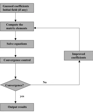
Figure 1.1: Scheme of Hartree Fock SCF calculation
23
Figure 2.1 Schematic representation of an SCF procedure Guessed coefficients
Initial field (if any)
Compute the matrix elements
Solve equations
Convergence control
Convergence?
Output results
Improved coefficients
yes
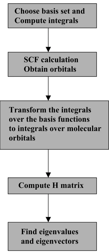
Figure 1.2: Flowchart for combined Hartree Fock SCF-CI method.
25
Choose basis set and
Compute integrals
SCF calculation
Obtain orbitals
Transform the integrals
over the basis functions
to integrals over molecular
orbitals
Compute H matrix
Find eigenvalues
and eigenvectors
Chapter 2
: Background on SiO
2topics.
2.1 SiO
2/Si in the semiconductor industry
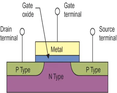
The Si-based Metal-Oxide-Semiconductor-Field-Effect-Transistor (MOSFET) was first
demonstrated in 1960. Since then it has driven the semiconductor industry for decades [1],
and enabled Ultra-Large-Scale-Integration (ULSI) [2]. Shown in Fig. 2.1 is a MOS transistor
structure. It consists of a Si substrate and a top gate electrode separated by an insulating SiO2
gate dielectric layer. The source and drain are deposited on the two sides to form a channel.
Carriers (electrons in n channel FET and holes in p channel FET) flow in the channel and are
tuned by applying a gate voltage. Since 1970s, the transistor density has doubled every 18
months, following Moore’s Law. As the dimensions of transistors decreased exponentially,
performance of microprocessors has improved regarding switching speed, delay time, and
power consumption [3-5].
SiO2 is made up of SiO4 tetrahedra connected at corners by oxygen atoms. Multiple
crystalline forms can be achieved depending on forming conditions. Suboxide forms exist,
but are not stable on Si. In industry, SiO2 can be easily formed by thermal growth or more
sophisticated methods such as Chemical Vapor Deposition (CVD). Such conditions generate
amorphous SiO2. These layers show ideal properties for integrated circuit (IC) applications,
including (1) high quality SiO2/Si interface with low density of interface states ~ 1-2 x 10¹⁰
(eV-cm2)-1, (2) a large band gap (~9eV), (3) thermal stability at high temperatures, and (4)
The application of SiO2/Si in the semiconductor industry made the material an interesting
research topic. The major topics include order parameter of the non-crystalline SiO2 phase
and various types of defect-sites.
For the order parameter, the focus is beyond the local tetrahedron. For a long period, the
glass phase was modeled as continuous random network (CRN). Restriction of the
orientation of neighboring SiO4 tetrahedrons was loose [7]. The introduction of
X-ray/Neutron Scattering techniques [8,9] provided new insight. Correlation between
neighboring SiO4 tetrahedrons are identified by bond angle distribution and length scale
beyond tetrahedron.
For defect sites, researchers applied various methods, such as luminescence [10], ESR
[11], Raman Spectroscopy [12], and XAS [13]. Point defects are the most intensively
studied, with various geometrical model proposed from different methods. Their
creation/activation under various conditions in the bulk and at the interface is examined. As
SiO2 is mixed with other dielectric materials and used in other applications such as optical
fiber, new conditions appear. Thus defect research is expected to continue.
As aggressive scaling continues, the SiO2/Si system faces limits. The transient time of
transistor switching, , is determined by the following equation:
(2.1)
where Cload is the load capacitance of transistor, VDD is the supply voltage, and ID,sat is the
saturation drain current. The saturation current ID,sat is then determined by
In the above equation, W is the channel width, L is the gate length, is the effective
mobility of charge carrier in the Si channel, Vgs is the gate-source bias, and VT is the
threshold. The scaling increases ID,sat by increasing the Cox, the oxide capacitance. The latter
can be expressed as
(2.3)
where is the dielectric constant of the gate dielectric (SiO2 in this case) and tox is the
thickness of the oxide. Thus reduced oxide thickness is desirable for faster reaction from
transistor. However this leads to increased gate-leakage current through the thin dielectric
layer [14].
2.2 Research on O-vacancy defects
The study of O-vacancy-related defects is an important topic in the Lucovsky research
group [15-21]. Various dielectric materials, such as HfO2 and HfSiON, are involved.
O-vacancy defects are important indicators of structural changes of the material during
processing.
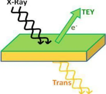
Previous study relies heavily on X-ray absorption spectroscopy. In such a process [22],
one electron from an inner shell of an atom is excited by a high intensity X-ray beam. It is
excited into an unoccupied state. Other electrons sense the core hole left over by the first
electron and fill it by subsequent downward transition. This process provides rich
The total electron yield method (TEY) is applied in our research (shown in Fig.2.2).
Samples are mounted on a metal plate in a high-vacuum chamber. During the X-ray process,
electrons are ejected out of the material and collected. To hold the sample electrically neutral,
electrons come into the sample from the plate. This forms a real time current, which is
proportional to the total transition intensity of the X-ray process. By tuning the X-ray energy
to the right range (OK edge for example), virtual states from normal and defect structure are
probed. The signal observed in the energy region just under the conduction band edge is what
inspired the calculation and subsequent experiments.
2.8 References
[1] K. Saraswat, C. O. Chui, K. Donghyun, T. Krishanmohan, A. Pethe, IEDM Tech. Dig.,
(2006) 659-662.
[2] S.M. Sze, Physics of Semiconductor Devices, 2nd Edition. (1981).
[3] S. Thompson, P.Packan, and M. Bohr, Intel Tech. Journal 2. Q3(1998).
[4] Y. T. Hou et al., IEDM Tech. Dig.,(2002).
[5] S. Borkar, IEEE Micro 19, 23 (1999).
[6] T. Hori, Gate dielectrics and MOS ULSIs (1997)
[7] YH. Tu et al,. Phys. Rev. Lett. 81. 22. 4899-4902(1998).
[8] J. Neuefeind, KD. Liss,. Berichte Der Bunsen-Gesellschaft-Physical Chemistry Chemical
Physics 100. 8. 1341-1349(1996).
[9]J. Du and L. Rene Corrales, Phys. Rev. B, 72(092201), (2005).
[11] J. Vitko, J. App. Phys. 49, (1978)5530-5535.
[12] JC. Mikkelsen, FL. Galeener, J. Non-Cryst. Solids. 37.(1980). 71-84.
[13] G. Lucovsky et al. Microelectric Engineering 88.(2011)1537-1540.
[14] G. B. Rayner, Jr., D. Kang, and G. Lucovsky, J. Vac. Sci. Technol. B. 21 1783(2003).
[15] G. Lucovsky, IEEE, 2006(148-159).
[16] G. Lucovsky et al. J. Mater. Sci: Mater. Electron. 18 (2007) S263-S266.
[17] G. Lucovsky, L. Miotti, and K. P. Bastos, J. Vac. Sci. Technol. B. 29(2011) 01AA01.
[18] G. Lucovsky, L. Miotti, and K. P. Bastos, Jpn. J. Appl. Phys. 50 (2011) 04DA15.
[19] G. Lucovsky, Jpn. J. Appl. Phys. 50(2011) 04DC09.
[20] G. Lucovsky, D. Zeller, K. Wu, and J. L. Whitten, Microelectronic Engineering
88(2011) 1537-1540.
[21] G. Lucosky, L. Miotti, and K. P. Bastos, Jpn. J. Appl. Phys. 50(2011) 10PPF04.
Chapter 3
: The SiO
2defect: case study.
As mentioned in the previous chapter, Lucovsky et al.[1] reported both singlet and triplet
signals in XAS pre-edge data. Dr. Lucovksy proposed a vacated-site model, featuring a weak
Si-Si bond instead of Si-O-Si bonding, to explain this phenomenon. This geometrical model
is the defect structure that this part of calculation addresses.
Two major issues are of interest here. First is the possibility for both singlet and triplet
transitions to appear in the data. This would require comparable energy levels for the lowest
singlet and triplet states of the defect site. Also the transition from the singlet and triplet
lowest state needs to be explored, especially in the range within the band gap. Since its signal
would not be buried by normal SiO2 band transitions, if the mentioned site reaches some
density high enough it could in principle be detected. To assess this quantitatively, a valid
geometrical model first needs to be established.
Thus this chapter is naturally divided into three parts.
1) The procedure to define the geometrical basis for a-SiO2. It includes optimization of
the bond length and bond angle and incorporation of medium range order into the system.
2) The behavior of the lowest singlet and triplet states, the interpretation and confirmation
that mixed occupancy would be possible. Since the dangling bond interaction mainly
involves two orbitals, the gap between the two states is broken down into different factors.
3) The behavior of the excitation for both spin-multiplicities. Excitation is calculated and
located in the bandgap region of a-SiO2. Peaks are categorized based on group theory. The
3.1 Structural basis for a-SiO
2 .3.1.1 Local parameters: bond length and bond angle
Construction of the structural basis of a-SiO2 starts with local parameters. In this material
it is well known that Si atoms are bonded to four neighbors in a tetrahedron setting. Also, the
two neighboring tetrahedrons maintain a staggered configuration. Thus the Si-O bond length
and Si-O-Si bond angle need to be tested.
Shown in Fig.3.1 is the scheme adopted from previous research [2]. It provides the
means to obtain optimized local parameters in a “strain free” environment. In our case, the
system is terminated by H atoms instead of Si “pseudo” atoms.
Optimization is done with respect to the total energy of the system. To reduce the amount
of work needed to find the optimized geometry, the parameters are changed alternatively. In
other word, a series of geometries with identical bond angle αbutdifferent O-Si bond length
are calculated. The optimized bond length is then picked up for a new series of geometry
with different bond angles.
After iterating the calculation, the results obtained are plotted in Fig.3.2 and 3.3 for bond
length and bond angle, respectively. The optimized value of bond angle and bond length is
148° and 1.595Å, respectively.
Since SiO2 has been studied for long time, various accounts exist for the two parameters.
A previous calculation [2] has already done a broader scan on the angle. The result is
cited in Fig.3.4, where d-polarization means the inclusion of Gaussian functions to represent
the d orbitals of Si and O. The results show good agreement.
Shown in Fig. 3.5 is the measured bond lengths of various forms of SiO2 [3]. Both
temperature and thermal expansion are considered. The bond lengths cover a range of 1.610
~ 1.615 Å. Even though our model is static, the bond length that we obtain, 1.595Å, is
reasonably close.
3.1.2 Medium Range Order.
With the local order defined, the next step is to obtain a big enough cluster to mimic bulk
SiO2. Even though a-SiO2 does not have long range order, the first sharp diffraction peak
from X-ray scattering reveals some characteristic lengths [4], which are attributed to Si-O
and O-O distances extending beyond nearest neighbors.
This is referred to as Medium Range Order (MRO). To represent this we need two layers
of Si tetrahedrons on each side of the oxygen atom if "bulk" influence is to be included. That
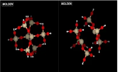
leads to the construction of a larger cluster, as shown in Fig.3.6. In the figure, Si and O
atoms are colored grey and red respectively. As in the previous case, the cluster is terminated
by the hydrogen atoms, which are shown as white in the figure.
The requirements of MRO can be satisfied by multiple geometries with the same number
of atoms involved. For two neighboring tetrahedrons, only the bond angle and staggered
configuration (dihedral angle) needs to be fixed. Thus a two tetrahedron cluster (as the
tetrahedrons, there are choices for their orientation. A staggered configuration means that
between the two neighboring tetrahedrons, four bonds would be in the same plane. When the
other four bonds are projected onto this plane, they appear on the opposite side of the line.
To define a plane, only two bonds are needed. Thus for each of the outside tetrahedrons,
there exist three planes for the choice of orientation. Because one Si-O bond on central
tetrahedron is involved for the connection, the plane can be defined by the selection of one
back bond connected to the same central Si atom.
If the Si-O-Si bond angle is 180º, the back bonds on two directly connected Si
tetrahedrons would pair up naturally in planes. Thus the three planes mentioned above would
only lead to one orientation. For our optimized angle, it is not the case. Tetrahedrons defined
by different planes are not equivalent. Even with the same plane, the same bond angle would
allow two different orientations. One bond can be bent upwards or downwards if we assume
the other Si-O bond in the Si-O-Si connection is horizontal. Thus when the orientation of the
central two tetrahedrons are fixed, there are six possible orientations by which one outside
tetrahedron can be attached onto one Oxygen atom. For the same number of atoms, the
number of alternative configurations is huge. And since silica is amorphous, there is no
specific reason to favor one configuration over another. The one used here is made such that
no specific symmetry axis could be found and the outside tetrahedrons are well spaced.
3.1.3. Band transition.
One obvious way to test the validity of this model is to calculate a “band transition”. The
ground state calculation of the system shows that the orbitals representing the nonbonding
“lone pair” electrons on O atoms have the highest energies. Therefore it is natural to expect
transition from such orbitals to represent the lowest-energy band transition.
The transition from the central O atom is calculated using localization and ion setting.
Since the ground state is singlet, the band transition energy is calculated as the energy
difference between the ground state and next singlet state. We obtained a value of 9.1eV,
reasonably close to experiment [5].
The orbital that the lone pair electron is excited into is diffused and involves Si 3d
orbitals from the central Si’s. This transition has a calculated dipole moment of nearly zero,
in good agreement with the concept of an indirect band gap.
3.2 Ground state of the defect site.
The defect site of interest here is a single oxygen vacancy, termed a vacated-site. There
can be multiple ways to "relax" the system after the central oxygen atom has been removed.
As proposed by Dr. Lucovsky [1], the two sides are realigned to make dangling bonds
colinear . It mimics the case of weak Si-Si bonding created during deposition or relaxation of
strained Si-O-Si bonding when the O atom is removed in post-deposition process. The central
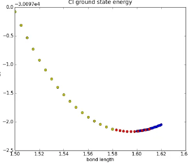
For the vacated-site, the energy of the lowest singlet and triplet is calculated with respect
to Si-Si distance and the result is shown in Fig.3.7. It can be seen that the gap between the
lowest singlet and triplet states decreases rapidly with increasing distance d.
The different behavior of the states can be explained by wavefunction formation at
configuration interaction level. The configurations involved in the singlet and triplet lowest
states differ mainly in the orbitals for the two electrons in the middle of the system. There are
two individual orbitals for electrons to occupy, one “bonding”(A1g) and one
“anti-bonding”(A2u) , as shown in Fig.3.8. They are denoted as σ and σ*. Thus the two
wavefunctions can be expressed as
)) 2 ( ) 2 ( ) 1 ( ) 1 ( det( ! )) 2 ( ) 2 ( ) 1 ( ) 1 ( det( ! * * 2 1
sin
N C N
C
glet
(3.1)
and )) 2 ( ) 2 ( ) 1 ( ) 1 ( det( ! )) 2 ( ) 2 ( ) 1 ( ) 1 ( det( ! * * N C N C
triplet
(3.2)
The “” in Eq.3.1 and 3.2 stands for all other doubly occupied orbitals that the singlet and
triplet have in common and α, β are spin wavefunctions. The C’s are coefficients for
normalization of the total wavefunction. In general, C1 is greater than C2.
By applying the above formation to the general equation
H
H (3.3)
and solving for the energy, the total energy of the system can be broken down into
different parts.
(1) (2) 1 (1) (2) (1) (2) 1 *(1) (2)
12 * *
12 *
0 *
r r
E E E
E (3.4)
Here, Eo stands for the total energy, including kinetic, nuclear attraction and electronic
repulsion, among all the other doubly occupied orbital without interaction with σ and *,
which can be written as
det(
)
det(
)
)!
2
(
1
0
H
N
E
(3.5)where E is the summation of the kinetic energy of nuclear attraction for
and electronicrepulsion between
and orbitals other than
*.
) 2 ( ) 2 ( ) 1 ( 1 ) 2 ( ) 1 ( ) 1 ( ) 2 ( ) 1 ( ) 1 ( 1 ) 2 ( ) 1 ( ) 1 ( ) / ( 12 12 2 i i i i k ik k r r r Z E (3.6) *E , whose formation differs from Eq.3.6 only by a subscript (from
to
*), is thecounterpart for
*. The last two terms, Coulomb and exchange term as commonly phrased,stand for the electronic repulsion between electrons in
,
*. Notation J is adopted forrepulsion terms in which same electron from both wavefunctions occupies the same spatial
orbital. Notation K is adopted for repulsion terms in which the same electron occupies
different spatial orbitals in the two wavefunctions. Subscripts are added to indicate the
spatial orbitals involved. So the last two terms in Eq.8 would be conveniently written as J*
Thus for the singlet, the total energy can be expressed as
0 * * * * * * )2 2 *
2 1 2 1 ( ) ( 2 1
E J J E J E J K
E E
E (3.7)
In the above equation, the first four terms treat the total wavefunction as equally
distributed between the two determinants without interaction. The last term adjusts the
energy based on the energy difference and interaction between determinants so that the
change of coefficients for determinants is factored in.
Fig.3.9 shows the behavior of E(lower curve) and E*(upper curve) with respect to
Si-Si distance d. The former increases rapidly with d, while the latter lingers within a range
of 1eV. This is a natural result of their electron density distribution.
Fig.3.10 shows the behavior of J(solid line),J * *(solid line with dots)and J*(dash
line). Those three terms all have orbitals occupied twice by the same electron from the
wavefunction on both sides.
For example,
* * 1 2
12 ) 2 ( ) 2 ( 1 ) 1 ( ) 1 (
* drdr
r
J
(3.8.a)Since spatial orbitals are normalized by themselves, the behavior of these terms follows
the 1/r factor and the change is much smaller than that seen in Fig.3.9
Fig.3.11 shows the energy ofK*(lower curve) and the square root term in Eq.3.7.
1 2
* 12 * ) 2 ( ) 2 ( 1 ) 1 ( ) 1 (
* drdr
r
Here, the same electron from different wavefunctions occupies different orbitals. Its value
and range are smaller than the J’s due to smaller overlap of from the electrons. However, due
to the shrinking gap between E andE*, it is still the dominating factor for the square root
term as d increases.
After all the individual terms related to σ and σ* are laid out, Fig.3.12 shows their
combined effect as E-Eo for both singlet and triplet. The E0, the contribution from all other
electrons are also shifted and plotted as a comparison.
The singlet and triplet behaviors are influenced by many factors. But the terms that
determine the singlet-triplet gap involve primarily the two central orbitals. Conceptually, the
two are generated from the interaction between dangling bonds from neighboring Si atoms.
Thus the two orbitals, and all the terms involving them depend on the overlap of the
wavefuncions from both sides. This implies the behavior of the gap does not only depend on
Si-Si distance d, but also on bond angle. Compared to other orientations, the vacated-site
should have larger gap due to maximized wavefunction overlap for a given angular
orientation.
A vacancy site where dangling bonds are kept at the normal Si-O-Si angle is tested and
the result plotted with vacated-site for comparison in Fig.3.13. A smaller gap is seen but the
difference is negligible in the range where the gap is small. It confirms the above argument
and also shows that at large distance, d is still a primary indicator of overlap since the
The gap calculated here cannot be measured by direct optical excitation because of spin
mismatch, but it can be used to estimate the ratio of occupancy between the triplet and singlet
by thermal excitation which is about3 ( )
B
E Exp
k T
, where E is the gap between the two
states and kB is Boltzmann constant. The factor 3 comes from the spin multiplicity. At the
annealing temperature, roughly 1200K [1], the factor is close to 1 for a gap of ~0.1eV, which
corresponds to the right end in Fig.3.7. It is likely that the small gap between the singlet and
triplet in this range results in both states being occupied, which leads to an excitation
spectrum from both states.
Due to the difference in geometries, it is impossible to compare the ground states of
normal a-SiO2 and vacated-site configurations directly. However, we can estimate these from
the SCF orbital energy. It is the summation of kinetic energy, nuclear attraction and all the
electron repulsion terms for a spatial orbital (defined by Fock operator in Chapter 1). Band
transition for silica starts from a lone pair electron on an Oxygen atom, whose orbital energy
is about 11.9eV. At 4.7Å, and * have orbital energies of 8.9eV and 7.74eV,
respectively. Eq3.1 shows that in the singlet an electron occupies some hybrid orbital
between and *
, thereby lowering its energy. Thus the singlet is at most 3eV higher than
the lone pair at the top of valence band.
3.3 Excitation for both singlet and triplet.
The excitation, both singlet and triplet, can be understood in terms of their atomic origin
Starting from Si atomic orbitals, the tetrahedral (Td) bonding of Si atom with its O
neighbors will be explained. The symmetry then will then be distorted to be three-fold (C3v)
to demonstrate the effect of a “dangling bond” on a single Si atom. With two “dangling
bonds” aligned towards each other, the evolution of unoccupied (virtual) molecular orbitals
will be shown. They form the basis of the excitation in the defect structure. Some discussion
is also provided on the effect of the angle between the dangling bonds to give this analysis
additional generality. Finally, the influence of bulk (Medium Range Order) will be taken into
account by incorporating the second Si neighbors into the system.
3.3.1 Bonding of a Si atom
Shown in Fig.3.14 is an energy diagram of a single Si atom without any neighbor/ligand
field. The valence shell and core levels are separated energetically. Without influence from
any neighbor, the system is highly symmetric and would maintain high degeneracy of
orbitals, such as the Si 3d’s.
A simple Si(OH)4 structure can be used to illustrate the bonding interaction between the a
Si atom and its oxygen neighbors. Under tetrahedral geometry (Td) as shown in Fig. 3.15 (a),
the energy diagram of the system is calculated and shown on the left side of the energy
diagram in Fig.3.16. Individual orbitals are plotted and assigned group symmetry labels
according their shape.
Compared to Fig. 3.14, several differences can be noticed. The number of occupied
energy levels is increased due to the involvement of O and H atoms. The core levels, such as
combinations under Td symmetry, as shown in Fig.3.17 (a). But the lack of interaction among
them produces minimal splitting. Thus T2 and A1 representation maintain the same energy.
For the valence orbitals, the situation is different. Atomic orbitals from different atoms
are energetically close to each other and have significant overlap. They can show strong
mixing to form bonding molecular orbitals, as shown in Fig.3.17 (b). Mixing between
different atomic orbital types here depends on their overlap, which is reflected in their match
of group representation. Si 3p, O 2pσ and H s functions all form T2 representation by
themselves. This enables them to mix and form molecular orbitals belonging to the T2
representation.
Any distortion of the structure can further reduce the degeneracy allowed by the system.
An example is shown in Fig.3.15 (b), where one OH group of the structure moved away from
the Si by 1.0Å. The point group changes from Td to be C3v, and the result can be seen on the
right hand side of Fig.3.16, with the evolution of the T1/T2 representations shown by arrows.
The C3v symmetry allows a highest degeneracy of 2, so the E and A1 representations
maintain their identity, with some shift in energy.
3.3.2 Single “dangling bond” on Si
When the OH group in Fig. 3.15 (b) is completely removed from the structure, the energy
diagram is shown on the right side of Fig.3.18. As in Fig. 3.15 (b), the symmetry is still C3v
type, but there are a few qualitative differences.
The electrons and atomic orbitals associated with the OH group are absent from the new
core and valence level. It, however, does not alter the number of orbitals associated with Si.
The energy shift for most of them is also small. The only exception is that mixing between
the Si 3p and neighboring O 2p functions, where a T2 representation splits into one E and one
A1 representation, as shown in Fig.3.19. The energy of A1 is raised dramatically due to the
lack of bonding interaction in one direction. This molecular orbital becomes a singly
occupied HOMO, commonly referred to as a “dangling bond”.
One CI calculation is done on this configuration and the excitation is shown in Fig. 3.20.
The symmetry representation of ground and excited states are identified by symmetry
combination of occupied molecular orbitals, with the ground state being A1. Bar plots are
used to indicate the transition energy and dipole. Gaussian fitting is also applied to simulate
the measurement and help to identify degeneracy. In total, ten excited states are involved.
The lower nine of them simply excite the electron from HOMO. That electron moves into
virtual molecular orbitals from Si 4s, 3d and 4p, as indicated in Fig. 3.18. The highest one
excites one electron from the A2 orbital below HOMO and places the electron in the A1
orbital from 4s. In this case, the excitation probes all the virtual orbitals in Fig. 3.18.
3.3.3 Interaction between “dangling bonds”.
If two Si(OH)3 structures are considered in a staggered geometry, with the dangling
bonds pointed towards each other, the newly created Si(OH)6 system, as shown in Fig.3.21,
mimics the vacated-site structure in the silica bulk. The structure has D3d symmetry, which
from both sides also interact and form molecular orbitals according to the new symmetry, as
shown in Fig. 3.22.
Newly formed molecular orbitals are either symmetric or antisymmetric with respect to
the inversion operation. The former is denoted by subscript g and the later by u. The lowest
two orbitals (A1g and A2u) in this diagram correspond to the σ and σ* orbitals that are used to
describe the lowest singlet and triplet state of the cluster. From the one 4s orbital and five 3d
orbitals of each Si atom, a total of 12 virtual molecular orbitals are formed. Compared to
their C3v counterparts, they spread out over a wider energy range with roughly the same
center. The excitation of electron from the A1g/A2u mentioned above into them generates the
excited states for the system.
In many cases the excitation can be understood as if it were located primarily on one
atom, as done with Tanabe-Sugano diagrams [6]. Even though the geometric center of the
structure is a vacancy, an analogy can be made by considering atomic orbitals with their
nucleus at the center of a D3d ligand field. Thus one set of p function gives one A2u (pz) and
one Eu representation. One function is an A1g representation and a set of d function gives a
A1g and two Eg representations. The full set of molecular orbitals on the right side of Fig.
3.22 would be equivalent to the combination of 2 s sets, one d set, two p sets and a separate
pz function. If a imaginary atom were to be placed in a D3d field such that its 2s, 2p, 3s, 3p,
3d and the pz functionfrom the 4p form a block of orbitals without the others, it would give
the same set of group representations. If two electrons are placed in the block, similar
As in large cluster, the system now has both singlet and triplet states. Their corresponding
lowest states could be expressed as
)) 2 ( ) 2 ( ) 1 ( ) 1 ( det( ! )) 2 ( ) 2 ( ) 1 ( ) 1 ( det( ! * * 2 1
sin
N C N
C
glet
(3.9)
and )) 2 ( ) 2 ( ) 1 ( ) 1 ( det( ! )) 2 ( ) 2 ( ) 1 ( ) 1 ( det( ! * * N C N C
triplet
(3.10)
where σ and σ* correspond to the lowest two molecular orbitals in Fig. 3.22, A1g and A2u
respectively.
Transitions from the singlet state are shown in Fig. 3.23 while the triplet counterpart is
plotted in Fig. 3.24. The singlet transition shows a total of 12 peaks. The lowest two are
made by simply rearranging the σσ+σ*σ* formation in Eq.3.9 into σsu/sgσ* configurations,
where su/sg stands the A2u/A1g at 1.2/1.6 eV in Fig.3.22, made primarily of 4s functions. The
rest are created by exciting the electron from σ* to a symmetric d orbital (red) or from σ to
anti-symmetric d orbital (black). For the triplet case, the first excited state in Fig.3.24 has the
σsg configuration as the major term. The ten excited states following it fall into two sets. The
lower five excite one electron from σ* to a symmetry orbital with 3d origin, while the higher
five replace the σ orbital in ground state with a anti-symmetric orbital with 3d origin.
In both cases, the inversion symmetry is altered during the excitation, as required by
group theory. Compared to the excitation from Si(OH)3, the range of d orbital-related
excitation expanded, which is consistent with the change in energy diagram shown in Fig.
3.3.4 Influence of bond angles.
So far, we have primarily addressed the geometry where the two Si dangling bonds are
collinear, forming weak Si-Si bonding. In amorphous SiO2, there are likely to be many
similar sites with different angles between the Si dangling bonds adjacent to the vacancy. It
is worthwhile to examine the impact of this angle.
If the angle between the two dangling bonds is not 180º, most symmetry operations under
D3d symmetry, such as inversion and three fold rotation, are no longer available. The only
symmetry operation that may still apply is the reflection (σ), if the two sides still maintain the
staggered configuration. In this case, the symmetry of the system is reduced to a simple Cs
group, which only allows the A’ and A” representations. In other words, degeneracy in
virtual orbitals and total wavefunctions would be completely removed. This does not
significantly alter the energy range of the virtual orbitals or total wavefunctions, as they are
primarily determined by their atomic origin.
As an example, the Si2(OH)6 cluster is slightly modified so that the dangling bonds from
the two Si atom form a angle of 148º. The new set of virtual orbitals is very similar to the set
shown in Fig. 3.22, except that the degeneracy have been removed. For instance, the Eg set at
~1.3 eV is now reduced to an A’ and an A”. Both occupy the same energy range but are
0.05eV apart.
The difference is more pronounced in the excitation spectrum for both singlet and triplet,
as shown in Fig. 3.25 and 3.26. For the ease of comparison, the arrows used in Fig. 3.23 and
Two differences can be seen. First, peaks similar to those in vacated-site case are seen,
with the degeneracy removed. This is in good agreement with the change of symmetry group.
Also, extra transition peaks show up with relatively weaker intensity. As discussed in the last
section, transition peaks under D3d symmetry are selected by parity. Since the inversion
operation is no longer applicable in the new symmetry, the parity restriction is gone.
Overall, the energy range of the transitions in the band gap is the same for the
vacated-site geometry, and the line shape is similar. Thus it is convenient to consider the vacated-vacated-site
since its high symmetry makes it easy to understand and the transitions from other similar
defect sites with unspecified bond angles may be approximated from the vacated-site case.
3.3.5 Influence of the bulk
So far, the analysis has been done for two Si atoms. As discussed when the cluster was
being established, the influence of bulk silica can be better estimated by adding six more
silicon tetrahedrons to mimic the medium range order of the material. An expanded cluster
with perfect D3d symmetry is shown in Fig.3.27. The inclusion of more neighbors is expected
to have two effects. First, it adds in Si 4s and 3d functions from newly introduced Si atoms to
form the molecular orbitals. Thus more virtual orbitals would be available for excited states.
Also the electronic potential each molecular orbital experiences would be altered.
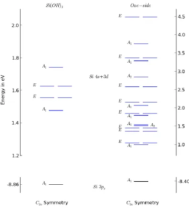
Following the analysis above, one-side of the cluster is considered first, with the energy
diagram shown in Fig. 3.28. Since each Si atom brings one 4s function and 5 3d function, a
total of 24 virtual molecular orbitals are constructed. Compared to the Si(OH)3 case, their
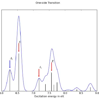
However, a CI calculation shows that the excitation, shown in Fig.3.29, has major peaks
similar to the Si(OH)3 case. This is a natural result of dipole selection. A dipole, as discussed
in the introduction of the algorithm, is calculated by the following equation,
e i g
i r
p
(1.11)
where subscripts g and e denote the ground and excited state respectively. Though Ψ
stands for the total wavefunction, it is easy to show that, for dipole to be nonzero, only one
molecular orbital can differ between the initial and final state. The expression holds if the Ψ
is replaced by the individual molecular orbitals by which the initial and final state differ.
In the specific case here, the orbital for initial state would be the “dangling” Si pz. A
comparison between the energy diagram for Si(OH)4 and Si(OH)3, as in Fig. 3.18, reveals
that a dangling bond orbital is separated energetically from the Si 3p bonding orbitals and O
2pπ orbitals. So when new Si neighbors are added, the dangling A1 orbital would remain
largely localized on one Si atom due to minimal mixing with new neighbors. For the dipole
in Eq.3.11 to be non-zero, the molecular orbital in final state needs to occupy the same
spatial area as pz.
This requirement is best satisfied when the electron is excited into a orbital made of Si 4s
and 3d function from the same Si atom as A1. Since molecular orbitals are linear combination
of atomic orbitals, there is only a limited number of virtual obitals with the mentioned atomic
orbital as major component. This small set is similar to the set of virtual orbitals in Si(OH)3.
They form the final states that have the biggest dipoles. Thus the symmetry representation of
have non-zero dipole, but the value is dampened by limited spatial overlap. Their presence is
pronounced by additional weaker excitation closer to 9eV.
The same bulk effect is also observed in singlet and triplet transition for the whole
cluster. As in the transition from Si(OH)3 to Si2(OH)6, molecular orbitals from both sides
would interact with each other and form new molecular orbitals according to the new
symmetry. 48 virtual orbitals in 6 A1g, 2 A2g, 2 A1u, 2 A2u, 8 Eg and 8 Eu representations are
generated, doubling the number with respect to the one-side case. The excitation spectrum is
shown in Fig. 3.30 and Fig.3.31 for singlet and triplet respectively.
As in the one-side case, more excitation peaks show up in the spectrum after Si neighbors
are introduced. They populate the energy range close to band gap. Red arrows are used in
both plots to identify the main peaks that define the profile. These major peaks have a similar
combination of representations as in Si2(OH)6 case. But their energy and dipole are changed
as a result of the bulk influence. As mentioned in one-side case, introduction of Si
neighboring expand the energy range of the virtual orbitals. Therefore there are excitation
peaks beyond the 9.0eV cutoff for both singlet and triplet features. This is also a result of
bulk influence.
In a word, the energy range and symmetry representation of major excitation peaks are
largely determined by the interaction between the Si atoms next to the vacancy. The bulk
effect is seen as a modification of the major peaks and the introduction of weaker transitions
The effect of bond angle is also tested with the big cluster, as in the Si2(OH)6 case, the angle between the dangling bonds are changed to 148º. The corresponding singlet and triplet
result are presented in Fig. 3.32 and Fig. 3.33 respectively.
Again, the comparison involving the large cluster confirms the effect of symmetry
modification. For the major transitions allowed under D3d symmetry, the energy shifts and
degeneracy is removed. More minor transitions, forbidden under D3d symmetry, also appear
when the parity restriction no longer applies.
3.4 Summary of the calculation.
This chapter mainly answers two questions on the proposed vacated-site structure in
amorphous SiO2.
The first question is whether there exists a certain geometrical configuration that allows
the system to have lowest singlet and triplet states to be energetically close.
The answer is given by the ground state analysis, where the energy difference between
the lowest singlet and triplet states is broken down into different contributing factors. We
conclude that when the two Si atoms next to the O vacancy are far apart, interpreted here as a
distance larger than 4.9Å, it is likely that both states are be occupied. This distance is much
larger than the normal Si-Si distance in a Si-O-Si bonding (< 3Å). This implies that if the
structure is created out of strained Si-O-Si bonding, significant local structural relaxation is
involved.
The second question is about the possible single electron excitation from both spin
The major transitions excite one electron from bonding or
![Figure 3.1: Schematic of two tetrahedrons bonded together, from ref [2].](https://thumb-us.123doks.com/thumbv2/123dok_us/1197722.1150449/61.612.141.487.166.536/figure-schematic-tetrahedrons-bonded-ref.webp)