Copyright to IJIRSET www.ijirset.com 10591
Development of Microcontroller Based
Inexpensive Water Analyzer: A Photoelectric
Design Approach
Pravin K. Bhadane
1, Suchita P. Bhangale
2, Milan S. Hira
3 Head, Department of Electronics, Nowrosjee Wadia College, Pune, India 1Assistance Professor, Department of Electronics, Nowrosjee Wadia College, Pune, India 2
U. G. Student, Department of Electronics, Nowrosjee Wadia College, Pune, India3
Abstract: A water analyzer, based on a photoelectric sensor, has designed, built and tested. It is designed to record automatically the optical density of some constituents in water. Laboratory tests have proved the instrument is sensitive to detect small changes in color of water. Generally, these constituents can be either measured by the bulky and costly analytical instruments like HPLC, or by the traditional methods of chemical analysis. The authors of the present paper have attempted to design an inexpensive, portable instrument using microcontroller. The instrument is designed using different colored LEDs and photodiode. The LED and the PWM circuit have been designed to produce a stable and intense source of light. An operational amplifier based current to voltage convertor is connected in series with the photodiode to convert transmitted light into analog voltage. Conversion of analog voltage to digital data has done by I2C type ADC. The data from ADC has fed to AT89C51 microcontroller for further processing of optical density, its calibration and display on character LCD. The developed device is light in weight, portable and economical.
Keywords: Water Analyzer, LED, Photodiode, ADC, Microcontroller.
I.INTRODUCTION
A solution appears colored when it absorbs the electromagnetic radiation. There is a close relation between the color of a substance and its electronic structure [1]. A molecule exhibits absorbance of light in the visible or ultraviolet range, when radiation causes an electronic transition, raising the molecule from the ground state to an exited state. The production or change of a color is connected with deformation of the normal electronic structure of molecule. Irradiation causes variations in the electronic energy of the molecule containing one or more groupings with unsaturated linkages.
The colorimetry deals with the color absorbance by the molecules and its analysis. In this technique, determination of elements is based on the absorption of the visible and ultraviolet radiation. The basis of colorimetric method is the simple relationship between absorption of radiation and concentration of colored species in solution. It has high selectivity and used for determining metals in alloys, minerals and complexes [2].
Accurate and rapid methods for analysis are necessary in the fields like water quality control [3], pollution control, toxicology [4], medical [5], and forensic sciences. In the past few years, analysts have developed many instrumental techniques. Among these techniques, colorimetric technique occupies a unique position because of its precision, accuracy and rapidity [6, 7].
Copyright to IJIRSET www.ijirset.com 10592 by using appropriately designed signal conditioning circuit. The automation in measurement and analysis improves rapidity.
In this paper, a low-cost colorimetric method for water analysis is presented, which combines modern semiconducting devices for the measurement, and advanced microcontroller for the analysis. The system can be used for the automatic analysis of water based samples and has the applications in the area of clinical diagnosis [10].
The rest of the paper is organized as follows. Section II provides a description of electronic circuit, the working of circuit is explained in section III. The experimental work is discussed in section IV, followed by the results and discussions in section V. Section VI gives basic algorithm. Finally, conclusions and some of our thoughts for future directions are presented in section VII.
II.ELECTRONIC CIRCUIT DESIGN AND DESCRIPTION
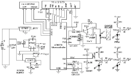
The electronic circuit designed for the water analyzer consists of four basic units- photoelectric sensor, signal conditioner, signal processing unit, and power supply (see figure 1).
Fig.1 Electronic circuit of microcontroller based photoelectric water analyzer
A. Photoelectric sensor
It is based on Beer- Lambert‟s law [6]. It deals with relationship between transmittance or absorbance of light and concentration of an absorbing species. It is made from the following units. (1) light source (2) sample holder and (3) detector, as shown in figure 2.
Fig. 2. Photoelectric unit with LED and photodiode. Details of each unit are given below:
1) Light Source: For absorption spectrometry, it is radiation source, while for emission spectrometry, it is excitation
Copyright to IJIRSET www.ijirset.com 10593 intensity (c) stable with no drift (d) should be relatively cheap (e) easily available.
For the visible range spectroscopy, tungsten filament lamp is an excellent light source. It produces wide range of radiation in the range 400 nm – 700 nm. The small portion of wavelength which is required for absorption by the analyte is selected from a wide range of spectrum with the use of monochromator such as optical filter, prism, or diffraction grating. The design of monochromator is complex, bulky and expensive. The modern type of high intensity LEDs can replace the above light source and monochromator. LEDs require less electric energy and produce monochromatic light. This makes power supply section compact and the instrument portable [8]. The use of LEDs as spectrally selective source of light in photometers was first described by Mims [11]. The normal rectifier diodes, made from silicon or germanium, are opaque and hence none of the light escape. On other hand LED uses semi-transparent material, which permits light to escape outside. By using elements like gallium, arsenic, and phosphorus, the energy gap can be controlled to yield radiation of different colors.
A typical spectral response of LED is shown in figure 3.
Fig. 3. Spectral response of typical LED.
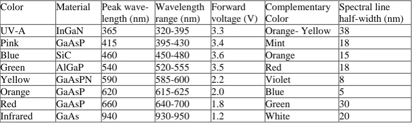
The Spectral Line Half-Width (SLHW) is the band width of this curve at 50% intensity. It is of the order of 10 to 50 nm, and it is a measure of monochromaticity of the LED. In the present study, ten watt LEDs of different colors have been used as source of light. The barrier potential of LED is in between 1.2 V to 3.6 V, the exact value depends on color and wattage. Typical specifications of LED are given in Table 1 [12].
TABLE 1:TYPICAL PARAMETERS OF LEDS AT 20MAFORWARD BIAS CURRENT
2) Sample holder: It is usually called cell or cuvette and it should not absorb the radiation. The most common cuvettes
for measuring visible and UV spectra are made of quartz, but they are expensive. The low cost glass cells are suitable for visible light measurement but not for UV spectra, because glass absorbs UV light while quartz is transparent for both UV and visible light. LED is fitted at one side of cuvette and its light is made to shine through the sample placed in cuvette. The transmitted light passed through the sample, struck the opposite side of the cuvette where photodiode is mounted.
3) Detector: It is used to turn a level of illumination into an electrical signal. The radiation detector must satisfy
Color Material Peak wave- length (nm)
Wavelength range (nm)
Forward voltage (V)
Complementary Color
Spectral line half-width (nm)
UV-A InGaN 365 320-395 3.3 Orange- Yellow 38
Pink GaAsP 415 395-430 3.4 Mint 18
Blue SiC 460 450-480 3.6 Orange 15
Green AlGaP 540 520-555 3.5 Red 18
Yellow GaAsPN 590 585-600 2.2 Violet 8
Orange GaAsP 620 615-625 2.0 Blue 5
Red GaAsP 660 640-700 1.8 Green 30
Infrared GaAs 940 930-950 1.2 White 20
Intensity(mcd)
Wavelength (nm) Imax
Imax /2
Copyright to IJIRSET www.ijirset.com 10594 following requirements: (a) broad wavelength range (b) sensitive to low levels of radiant power (c ) respond rapidly to the radiation (d) produce an electrical signal that can be easily amplified (e) high signal to noise ratio. The commonly used detectors are either photoconductive or solid state barrier layer type.
Photoconductive cell: It is a light dependant resistor (LDR) made of a material like CdS and PbS. The resistance of LDR depends on the intensity and wavelength of the light falling on it. The resistance varies typically between 10 MΩ (dark) to about 1 KΩ at 100 Lux. The variation in resistance (R) with intensity (I) is given by the relation [13],
log10 (R) = -K log10 (I) +C,
Where, K and C are constants which are dependent on wavelength and physical dimensions. LDR has the advantages of (1) long life (2) requires simple electronics.
Barrier layer cell: It is a very simple photovoltaic device which generates a voltage when its semiconductor type surface is illuminated. It is advantageous for its high sensitivity, good stability and no external source of electrical energy is required. In the present work, silicon photodiode (BPW 21) has been used as a detector. The wavelength range of BPW21 is 350-1100 nm and peak wavelength, λp of 565nm. It is ideal for low light level applications, where a very high signal to noise ratio is important. The device operates on the principle that irradiation of a p-n junction produce charge carriers known as electron–hole pairs. Once the number of photo-induced carriers exceeds those induced by the thermal process (dark current), the photocurrent is proportional to the intensity of incident radiation [13].
B. Signal conditioner
In present study it is I to V convertor. The light produced by LED is passed through the sample cell. The cell absorbs different amount of light depending on the type and concentration of material in the cell. A photodiode is mounted on the other side of the cell. As the transmitted light struck the photodiode, the electron-hole pairs are formed which leads to an increase in the photocurrent. It is necessary to convert current into voltage, because microcontroller requires input in the form of voltage.
An operational amplifier (OP-AMP) configured as I to V convertor for the conversion of photocurrent into a voltage. The IC CA3140 OP-AMP makes a good choice because of its very low input bias current (20 pA) and the input offset voltage (5 mV). The output voltage of converter is given by,
Vout = -Ipd X R4. Where Ipd is the photo current in µA, R4 is the feedback resistor.
Because some solutions under test may have very strong absorption characteristics, resulting in less transmitted light and small photocurrent. To amplify it to a sufficient level, large value of feedback resistor is required. While at the same time being able to measure the large currents corresponding to the highly diluted solutions. To balance the need of different gain values, variable resistor of value 1 MΩ is used in the feedback [14].
C. Signal processing unit
The signal processing unit has the job of signal acquisition and manipulating it in the form which is required by the readout system. The signal processing unit is a microcontroller system based on ATMEL AT89C51 [15], which is essentially a 8-bit microcomputer for the operations of data management and modification.
Readout device and user interface:The microcontroller has the function of analyzing and displaying data on the LCD. It is a character type 16 x 2 LCD which accepts the command and the data in ASCII format. The user interface has been provided by the 4 X 4 keypad. It is constructed from the push to on release to off type key switches. It is interfaced to port 0 of the microcontroller.
D. Power supply section [16] :
It includes three fixed voltage supplies, which are shown in figure 1. Details of them are given below.
+5 V dc power supply:-For microcontrollers, voltage fluctuation is fatal, in such situation to ensure constant voltage; IC 7805 voltage regulator is used. It is a 5V fixed three terminal positive voltage regulator IC. The IC has features such as short circuit protection, thermal shut down, internal current limiting, which makes the IC very rugged. It regulates a steady output of 5 V, if the input voltage is in the range of 7.2V to 35V. Output currents up to 1A can be drawn from the IC provided that there is a proper heat sink.
Copyright to IJIRSET www.ijirset.com 10595 voltage convertor IC 7660. With the connection of two 10 uF capacitors used for charge pump and storage, it performs the complete supply voltage conversion from +5V to -5V.
+12V dc power supply :- Fixed power supplies are available in different ranges but they provide very low current of one or two amperes, they can‟t drive high wattage LEDs. So, to overcome it, a high current power supply circuit has constructed from IC 317T, which can drive the load of high wattage LEDs. The current handling capacity can be increased by connecting 2N3055 power transistors in parallel with IC 317. The resistors are designed by formula,
V0=1.25 X 1+R2 R1
+Iadj X R2
Where, V0 = Output voltage, R1, R2 = Resistance values, Iadj = current through the ADJUST pin. The current through ADJUST pin is about 50 to 100 uA. So we may neglect the second term of the above equation. The value of R1 has to be kept small, about 220Ω. For 12V output, the R2 becomes 1892Ω. In the present work it is a preset of value 5KΩ.
III.WORKING OF CIRCUIT
The working of the circuit can be followed most easily through reference to the schematic diagram of the water analyzer in figure 1. In the photoelectric section of circuit, light from the LED falls on the sample placed in cuvette. The sample absorbs some part of light and the rest is transmitted for to be detected by the photo-diode placed on the other side of the sample holder. The current produced by the diode is converted in to voltage by the I to V amplifier. The output of the amplifier is fed into ADC. This component converts the analog voltage into digital form. The microcontroller program is written for the ADC operations such as start of conversion, wait till it is converted, when conversion is done then read digital data.
The microcontroller performs the calculations of optical density and concentration. It can be done either with the use of calibration curve or from the equation of line i.e. concentration is the ratio of optical density and slope. In the last section the display of result takes place. The data port of LCD is connected to the port 2 of the microcontroller. Enable, RW, and RS pins of LCD are connected to the Port 1. The schematic diagram and artwork were prepared in PSpice and OrCAD [17] software respectively.
IV.EXPERIMENTAL WORK
All the parts of instrument work together as follows (refer figure 1). LED produces a beam of light with a narrow band of energies. The intensity of the beam, I0, for the blank solution is measured by the microcontroller unit. The sample is then placed between the LED and the photodiode. If some of the light is absorbed by the sample, the intensity of the beam reaching the detector, I, will be less than I0. The detector compares the two intensities and reports the result as either transmittance (%T) or absorbance (A).
The fraction of I0 that gets through the sample is called Transmittance (T) is given by, T=I
I0
……….... (1)
It is practically difficult to detect absorbance, but it can be calculated from the transmittance.
A = - log10 T, A = log10 1 T= log10(
I0
I) ….… (2) T is also given by, T = 10 - ɛlc
Where: ɛ = molar absorptivity , l = path length of light beam (cm); c = concentration of absorbing species. log10T = log10 (10
- ɛlc
) = - ɛlc
A = - log10T = ɛlc………. (3)
In order to achieve the most accurate results of the concentration of colored species in solution, we need to maximize the absorptivity of the species. We must select the wavelength of light from our source that is best absorbed by the molecule. For example, if a solution is blue, it will absorb orange light, and the wavelength of maximum absorbance, λmax, will be 620nm (see Table I). In automated colorimeter it is easy to select the complementary color LED and plotting the absorbance versus the wavelength manually or let the instrument scan through the range automatically, and perform curve fitting. From the plot we can determine the exact wavelength of the complementary color, which is the wavelength of the maximum absorbance (λmax).
Copyright to IJIRSET www.ijirset.com 10596 Concentration
(X1,Y1)
(X2,Y2)
Slope, m =Y2 − Y1 X2 − X1
OD
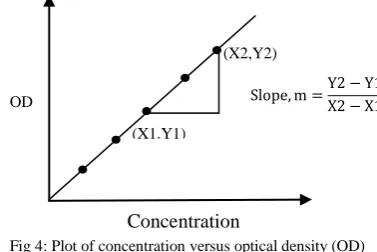
absorbance is also called optical density (OD). Since ɛ and l will not change, they can be combined into a new constant, k. Thus, A = kc. It can be compared with the equation of a straight line,
y = mx + b
Where, y = A, x = c,m=kandb = 0, m is slope of the line, andbis they-intercept. Beer‟s law then states that a plot of absorbance verses concentration will give a straight line passing through the origin. The slope of the line depends upon the constituents of solution, and it is required for the calculation of unknown solution.
There is no direct mathematical relationship between absorbance and concentration. To find the concentration of unknown solution, it is necessary to plot the calibration curve. This curve is called a Beer‟s Plot [18] which is shown in figure 4. The unknown concentration of colored species in solution can be obtained from the calibration plot.
Fig 4: Plot of concentration versus optical density (OD)
V.RESULTS AND DISCUSSION
Five different concentrations of copper sulphate solutions were prepared. Using highest concentration solution of copper sulphate, λmax was determined and it was found to be 625 nm. At this λmax, optical densities of different concentration solutions of copper sulphate as well as unknown concentration solution of copper sulphate were measured and are depicted in the Table II. The graph of concentration verses optical density is shown in figure 5.
Concentration of CuSO4, M Optical density at λmax = 625 nm
0.010 0.34
0.008 0.29
0.006 0.21
0.004 0.13
0.002 0.07
Unknown 0.16
Table II. Observations of optical density for the known concentrations of CuSO4.
Fig. 5 : Calibration curve for finding out concentration of unknown solution.
For a given unknown solution the measured optical density is 0.16. The concentration of unknown solution is determined from the calibration curve as shown in the above figure. The value of unknown concentration from the
0 0.05 0.1 0.15 0.2 0.25 0.3 0.35 0.4
O
p
ti
ca
l
D
en
si
ty
Copyright to IJIRSET www.ijirset.com 10597 curve is found to be 0.005 M.
VI.SOFTWARE
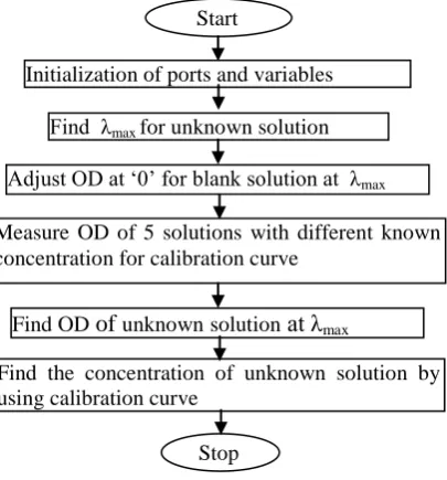
Figure 6 shows the flowchart of the optical density (OD) computation program. The steps involved in the measurement of transmitted light and its conversion into OD are shown in the flowchart.
Fig.6. Flow chart of the optical density measurement.
The software program has been developed in the C language. The source code is compiled in Keil [15] IDE, and programmed into microcontroller AT89C51 with the help of µC-flash programmer. Soft copy of the source code can be obtained freely from the authors.
VII.CONCLUSIONS
Handheld colorimeter with light emitting diode is a new kind of inexpensive instrument that provides much better long term stability than instruments that uses expensive and optically unstable filament lamp and monochromator. However, the wide SLHW bandwidth of LED e.g. about 30 nm for red LED poses some challenges in accuracy and precision. The use of photodiode in place of photoconductive cell has significant advantages, including low cost and durability. The use of high intensity LEDs as source of light provides enough sensitivity to measure the optical density of relatively dilute solutions. In addition, the system has attractive features, such as no need of optical filters, automatic measurements of λmax, generation of calibration curve, calculation of the optical density and concentration of unknown solution. Therefore, rapid and accurate analysis is possible. The designed equipment has been successfully used for the measurement of concentration of CuSO4 in water solution. Similarly it can be used for other constituents of water such as cyanide, iron, and fluoride by forming their complexes.
Future scope: The colorimeter will be optimized for the better accuracy and precision with the use of multiple photodiodes, and narrow viewing angle type high intensity LEDs. Similarly, the rapidity will be improved by use more advanced microcontroller and signal conditioning circuit.
ACKNOWLEDGMENT
Authors are thankful to the Principal, N. Wadia College, Pune, for providing the laboratory facility. Adjust OD at „0‟ for blank solution at λmax
Start
Stop
Initialization of ports and variables
Find λmax for unknown solution
Measure OD of 5 solutions with different known concentration for calibration curve
Find OD of unknown solution at λmax
Copyright to IJIRSET www.ijirset.com 10598
REFERENCES
[1] H. Zolliger, Color Chemistry: Syntheses, Properties, and Applications of Organic Dyes and Pigments, 3rd ed., Wiley-VCH, 2003.
[2] J. B. Brady, J. D. Frantz, “Microanalytical technique for determination of aluminum in aqueous solutions,” American Mineralogist, vol. 65, pp. 1249-1251, 1980.
[3] Y. Suzuki, M. Endo, J. JIN, K. Iwase, and M. Iwatsuki, “Tristimulus Colorimetry Using a Digital Still Camera and Its Application to Determination of iron and Residual Chlorine in Water Samples,” Analytical Sciences, vol. 22, pp. 411-414, 2006.
[4] U. Itodo, A. Usman, S. B. Sulaiman, H. U. Itodo, “Color Matching Estimation of Iron Concentrations in Branded Iron Supplements Marketed in Nigeria,” Advances in Analytical Chemistry, vol. 2(1), pp. 16-23, 2012.
[5] Balas, “An Imaging Colorimeter for Noncontact Tissue Color Mapping,” IEEE transactions on biomedical engineering, vol. 44(6), pp. 468-474, 1997.
[6] A. Skoog, D. M. West, F. J. Holler & S. R. Crouch, Fundamentals ofAnalytical Chemistry, 8thEdn., Thomson-Brooks/Cole, 2004. [7] Z. Marczenko, Separation and Spectrophotometric Determination of Elements. John Wiley and Sons, New York, 1986.
[8] R. Brooks, F. M. Mims III, “Development of an inexpensive handheld LED-based Sun photometer for the GLOBE program,” Journal of
Geophysical research, vol. 106 (D5), 4733-4740, 2001.
[9] S. W. Brown, C. Santana, and G. P. Eppeldauer, “Development of a Tunable LED-Based Colorimetric Source,” J. Res.Natl. Inst. Stand.
Technol., vol. 107, pp. 363–371, 2002.
[10] T. R. Clem and R. H. Yolken, “Practical colorimeter for direct measurement of microplates in enzyme immunoassay systems,” J. Clin. Microbiol., vol.7(1), pp. 55-58, 1978.
[11] M. Mims III, “Sun photometer with light- emitting diode as spectrally selective detectors,” Appl. Opt. vol. 31, pp. 6965-6967, 1992. [12] R. A. Day, and A. L. Underwood. Quantitative Analysis, 3rd ed., Englewood Cliffs, NJ: Prentice-Hall, Inc., 1974.
[13] B. G. Streetman, S. Banerjee, Solid State Electronic Devices, 6th ed., PHI, New Delhi, 2002.
[14] “Circuit note CN-0312 data sheet,” Analog Devices, Norwood, MA, USA.
[15] M. A. Mazidi, J. G. Mazidi, The 8051 Microcontroller and Embedded Systems using Assembly and C, 2nd ed., Prentice Hall, 2000.
[16] A. Malvino, D.J. Bates, Principles of Electronics, 7th ed., Tata-McGraw Hill, 2000.
Copyright to IJIRSET www.ijirset.com 10599
BIOGRAPHY
Dr. Pravin K. Bhadane is Head of the Electronics Department at Nowrosjee Wadia College, Pune (India). He has obtained the M.Phil. and Ph.D. degrees from University of Pune. He is a author of more than ten research papers and two text books. His research interest is in the field of analytical instrumentation.
Prof. (Mrs) Suchita P. Bhangale is working as a Assistant Professor of Electronics at Nowrosjee Wadia College, Pune (India). She has done M.Sc. in Electronics and now pursuing her research in the field of analytical instrumentation.