Mixed-Phase (2H and 1T) MoS
2
Catalyst for a
Highly Efficient and Stable Si Photocathode
Jemee Joe,†, § Changdeuck Bae,†, §,* Eunsoo Kim,† Thi Anh Ho,† Heejun Yang,† Jong Hyeo k Park,‡ * and Hyunjung Shin†,*
†Department of Energy Science, Sungkyunkwan University, Suwon, South Korea
‡Department of Chemical and Biomolecular Engineering, YonSei University, Seoul 120-749,
South Korea
§ These authors contributed equally to this work.
* To whom correspondence should be addressed. C.B. ([email protected]), J.H.P
([email protected]) and H.S. ([email protected])
Abstract
We describe the direct formation of mixed-phase (1T and 2H) MoS2 layers on Si as a photocathode via atomic layer deposition (ALD) for application in the photoelectrochemical
(PEC) reduction of water to hydrogen. Without typical series-metal interfaces between Si and
MoS2, our p-Si/SiOx/MoS2 photocathode showed efficient and stable operation in hydrogen evolution reactions (HERs). The resulting performance could be explained by spatially genuine
device architectures in three dimensions (that is, laterally homo and vertically heterojunction
structures). The ALD-grown MoS2 overlayer with the mixed-phase 1T and 2H homojunction passivates light absorber and surface states and functions as a monolithic structure for effective
charge transport within MoS2. It is also beneficial in the operation of p-i-n heterojunctions with inhomogeneous barrier heights due to the presence of mixed-phase cocatalysts. The effective
barrier heights reached up to 0.8 eV with optimized MoS2 thicknesses, leading to a 670 mV photovoltage enhancement without employing buried Si p-n junctions. The fast-transient
behaviors via light illumination show that the mixed-phase layered chalcogenides can serve as
efficient cocatalysts by depinning the Fermi levels at the interfaces. A long-term operation of
Introduction
The photoelectrochemical (PEC) splitting of water into oxygen and hydrogen offers green fuel
from solar energy. It requires a semiconductor to absorb photons of visible light and to generate
excitons, fast charge separation within the depletion layer followed by efficient charge transfer
to the electrolyte. Employing thin layers of cocatalysts onto semiconductor surfaces can alter
the surface energetics by bending the degree of energy bands and/or charge transfer kinetics.1 By choosing suitable catalytic systems, moreover, the semiconductor can be protected from the
solution environment.2 Silicon (Si) has been spotlighted as a promising earth-abundant light absorber due to its small band gap of 1.12 eV and its viability in the electronic device industry,
especially in the field of solar cells. However, the corrosion stability3 along with the poor surface kinetics hinders its use as an efficient and stable photoelectrode. To produce real water
splitting on Si with good stability, therefore, surface protection is required. Much progress has
been made mostly by modifying the semiconductor surface with various cocatalysts. In general,
metals with a high work function (𝜙 ) are candidates because the barrier heights are increased;
thus, chemically inert noble metals are favorable. Platinum (Pt) and Pt-group metals are the
best-reported catalysts due to their large 𝜙 . Choi et al. decorated Pt particles on a silicon
surface with an Al2O3 protection layer, showing 12 h of stable operation with a 27 mA·cm-2
saturated current density (Jph).4 Zhao et al. modified silicon’s morphology into black silicon, followed by deeply burying Pt nanoparticles inside the wires, which showed a 0.434 V onset
voltage with a 22.5 mA·cm-2 Jph.5 Feng et al. fabricated a photocathode with series-metal
deposition of Ti and Ni thin films before a Pt catalyst on p-Si, which exhibited an onset potential
of ~ 0.3 V with a Jph of 30 mA·cm-2 and 12 h of operation in an alkaline solution.6
Among the various candidates, transition metal dichacogenides (TMD) materials have attracted
significant attention due to its unique physical, optical and electrical properties.7,8 The lack of dangling bond of the basal plane layer enables the photovoltage (Vph) be governed by the solid-state junction rather than its surface,9 which gives interest to many researchers to exploit the material to adapt in the field of photoelectrochemistry. Molybdenum disulfide (MoS2) is the most widely studied material since it is cheap, earth-abundant and exhibits exceptional stability
even in a strong acid,10 which makes the materials to be considered as an efficient catalytic material for the hydrogen evolution reaction (HER).11,12,13 Abundant structural defects (or edge sites) and high crystallinity and phase could lead to a highly active electrocatalyst.14 Various fabrication methods, including mechanical and chemical exfoliation, that expose more
edge sites of unsaturated S atoms have been studied.15 ,16 Oh et al. showed the improved crystallinity of MoS2 layer grown by atomic layer deposition (ALD), followed by sulfurization at high temperatures leads to better PEC performance, which are 630 mV reduction in the
overpotential over Si and 24 h of stable operation.17 It is found that the phase is the most affecting factors determining the electrocatalytic activity18 and the metallic 1T phase has shown much higher activity in HER compared to semiconducting 2H phase.19,20
More on this, in PEC where solid-state properties are concerned, the detailed device
configurations of semiconductor-based photoelectrodes has progressed: (1) Utilizing a
metal-insulator-semiconductor (MIS) Schottky junction structure with a cocatalyst has proven to
enhance the overall performance by modulating the band bending at the semiconductor surface.
Recent studies have shown that the photocatalyst layer on the semiconductor increases the band
bending, affecting the resulting Vph.21,22 The photocatalysts deposited on the semiconductor protect the surface from photocorrosion during an electrochemical reaction and secure
chemically active/reaction sites on the surface, improving the charge transfer kinetics between
semiconductor has been employed. Kwon et al. grew MoS2 layers on SiO2, followed by
transferring them to a Si substrate to form a p-n heterojunction, which exhibited a 24.6 m·Acm
-2Jph at 0 V vs. RHE with a 0.17 V onset potential.23 Seo et al. produced an onset potential of
0.36 V for a silicon photocathode with surface functionalization combined with Pt.24 Benck et
al. fabricated a silicon buried p-n junction with MoS2 as the cocatalyst and showed an onset voltage of 0.32 V.25 The presence of interfacial oxides, such as native SiOx, not only provides the passivation for semiconductor surface states but also alleviates Fermi level pinning
effects.26 Despite the synergetic roles of interfacial oxides in water splitting, the direct deposition of materials with a high 𝜙 on Si/SiOx causes stability issues for long-term operation. (3) Researchers have demonstrated that the introduction of series-metal thin films,
such as metal silicides, between Si and cocatalysts improved the stability. A Stanford University
group showed a stability of up to 100 h at 0 V vs. RHE by a thin MoxSi and Mo layers on a buried n+p junction. Fan et al. additionally introduced thin Al2O3 layers on a Si junction to improve the stability from photocorrosion.27 Although an amorphous Si-based photocathode with a high Vph of 0.8 V has been reported, this was attributed to the different band gap of 1.7 eV.28
Recently, we developed an ALD chemistry that can directly produce as-grown
crystalline MoS2 thin films on various substrates at low temperatures (250 - 300 °C) using inexpensive precursors (i.e., MoCl5 + H2S). ALD techniques have shown an exceptional capability for studying the critical thickness required for optimal HER operation.29 Here, we describe that mixed-phase (1T and 2H) MoS2 layers can be formed on Si as photocathodes via ALD for the PEC reduction of water. Note that we did not employed the extra phase-transition
procedure from semiconducting 2H to metallic 1T phase. Without utilizing conventional
operation during HERs. The present devices have spatially genuine architectures in three
dimensions (that is, laterally homo and vertically heterojunction structures). The effective
barrier heights reached 0.6 eV with optimized MoS2 thicknesses, leading to a Vph enhancement of 670 mV without employing buried Si p-n junctions. A long-term operation of ~ 70 h was
also demonstrated. We suggest that in general, 1T-2H mixed-phase layered chalcogenides could
serve as efficient cocatalysts by depinning Fermi levels at the interfaces, resulting in efficient
electron transfer mechanisms.
Results and discussion
Figure 1. Device configurations of Si-based photocathodes. (a) Typical
metal-insulator-semiconductor (MIS) Schottky junction photocathode with photocorrosion passivating and
adhesion-promoting metal layers beneath the cocatalysts. (b) Our simple p-Si/SiOx /mixed-phase (1T/2H) MoS2 photocathode with laterally homo and vertically heterojunctions that
includes an MIS junction inside.
in the depletion region, mainly inside p-Si, and then transferred through the tunnel oxide to the
thin metal interfaces toward cocatalysts in the electrolyte. The monolithic homojunctions
consist of mixed-phase 1T and 2H MoS2 that develop during the growth of MoS2 via ALD. Depending on the degree of distortion in the S-Mo-S atomic planes, 2H and 1T phases exhibit
different structural and electronic properties. The 2H phase has semiconducting properties and
is more stable compared to other phases (e.g., 3R and 1T), whereas the 1T phase is metallic
and unstable. A key mechanism may be the inclusion of an excess chlorine moiety along the
MoS2 basal plane upon incomplete reactions at low temperatures as probed by elemental analysis, X-ray photoelectron spectroscopy, and X-ray diffraction patterns.30 We also demonstrated that as a result of the presence of Cl, the 1T phase was stable upon thermal
annealing at 400 °C. Since the 1T phase of MoS2 is metallic, the resulting MoS2 layers as cocatalysts on the Si photocathode exhibit distinctively monolithic homojunctions with
changes in the Φ laterally along the interfaces, as illustrated in Fig. 1b. Our p-Si/SiOx/MoS2 photocathode makes the electron transfer pathway effective compared to a conventional MIS
electrode, eliminating additional processes that are required for complicated interface
engineering. Note that additional phase-conversion (2H-to-1T) and film-transfer processes
Figure 2. Preparation of p-Si/SiOx/MoS2 photocathodes via ALD as a function of
Cross-sectional TEM and (b) STEM images of 100 ALD-cycled MoS2 on Si; (c) SEM of 300 cycles; (d) SEM of 500 cycles; (e) SEM of 1000 cycles; (f) TEM of 300 cycles; (g) TEM of
1000 cycles showing a few layers of the MoS2 stacked together. (h-i) High-resolution XPS spectra of Mo 3d and (k) S 2p core level peaks, and (j) Raman spectra of MoS2 on Si. (k) Thickness as a function of ALD cycles, showing the linear growth rate.
The overall morphologies (Figs. 2c-e) and the resulting thicknesses (Figs. 2a-b, f-g,
and k) of MoS2 on Si surfaces were reproducible as previously reported.19 The layered-structural nature was shown by the Raman spectra (Fig. 2j), and the mixed-phase (1T and 2H)
structures were also observed via XPS spectra (Figs. 2h and i). Initial cycles up to 100 ALD
cycles resulted in several MoS2 nanoflakes (diameter of ~ 10 nm). Most of the nuclei layers have parallel basal planes to the substrate surfaces, as shown in Figs. 2a and f. The TEM of
300-cycled MoS2 shows more vertically grown MoS2 layers on the p-Si, as shown in Fig. 2f. This growth mechanism was observed in thicker layers (1000 cycles in Fig. 2g) and was
Figure 3. PEC performance of p-Si/SiOx/MoS2 photocathodes with different numbers of
ALD Cycles. (a) Current density (Jph) - voltage (V) characteristic of the photocathodes under 1 sun illumination at a reverse bias. Anodic shifts of up to 0.35 V for the onset voltage
(photocurrent onset of 0.1 mA·cm-2) were observed at approximately 500 cycles of ALD with a Jph of ~ 30 mA·cm-2. (b) Open circuit potential (OCP) measurement of our simple p -Si/SiOx/MoS2 photocathode for different MoS2 thicknesses in the electrolyte. Each sample’s OCP was recorded under dark and with 1 sun illumination. Red and black closed circles
represent illumination and dark equilibrium, respectively. Red open circles are saturated
voltages. The OCP shifted from positive to negative upon illumination, indicating the p-type
property of the substrate. As the thickness increased, the flat-band potential increased from 0.11
of ALD cycles. (d) Mott-Schottky plots of the p-Si/SiOx/MoS2 photocathode measured at reverse biases with a frequency of 200 kHz and a scan rate of 10 mV·s-1. The effective barrier heights of ~ 0.8 and 0.4 eV were estimated for 500 and 300 cycles, respectively.
We investigated the HER performance of our p-Si/SiOx/MoS2 photocathodes as a function of the MoS2 thickness under illumination (100 mW·cm-2), as shown in Fig. 3. For a bare p-type silicon treated with HF, a photoelectrochemical reduction process begins at an
onset potential of -0.12 V (which is defined when the photocurrent reaches 0.1 mA·cm-2) with a Jph of 24 ± 2 mA·cm-2, which is consistent with other studies.31 The corresponding measured
Vph is shown in Fig. 3b, which is 0.11 ± 0.04 V and is much less than the theoretical maximum
Vph of Si of 0.48 to 0.5 V.32 The gradual increase in Jph near the turn-on potential (shown in Fig. 3a (solid black line)) indicates the slow kinetics of the charge transfer processes. The
decreased Vph and the kinetics are attributed to the presence of surface states, followed by Fermi-level pinning (hereafter called FLPss)33,34 at the surface/electrolyte interface and by the build-up of a surface oxide layer23 and/or by electron traps by the complex surface chemistries that are associated with the formation of Si-OH bonds.35 The photocathode produced via a few tens of ALD cycles of MoS2 (data now shown) deposited on p-Si, which corresponds to less than 5 nm in thickness, showed negligible improvements in the PEC performance. This is partly
due to the incomplete coverage of the silicon surface area since, from the initial ALD cycles, a
number of seed layers of less than a few nanometer-thick nanoflakes randomly grow on Si. The
photocathode produced with 100 ALD cycles, which is ~ 7 nm in average thickness, achieved
an enhanced onset potential of 0.27 ± 0.02 V with an increased Jph of 27.5 ± 0.5 mA·cm-2. As
surface states being reduced by the MoS2 layers. The increase in a Jph compared to bare p-Si is due to the reduced surface recombination, which is one of the limiting factors for
photocurrents.36 As the number of ALD cycle increased to 300, an onset potential shift to 0.24 ± 0.03 V was observed with an increase in the Vph of 0.48 ± 0.01 V. As explained in our previous studies, after a certain number of flakes, additional MoS2 layers grow in the vertical direction, covering the remaining exposed silicon surface to passivate from the electrolyte.19 Consequently, the Fermi level effect was almost alleviated as Vph reached the maximum value for p-Si. The maximum Vph value of 0.80 to 0.67 V, which is much higher than the maximum Vph limit (V ) of p-Si and the Jph of 30 mA·cm-2 was attained at 500 ALD cycles (30 to 35 nm in average thickness). This is mainly attributed to the formation of a p-i-n
heterojunction, including MIS between the p-Si/1T-MoS2 partially within the bulk films, which will be discussed later in more detail. The kinetic improvement that was partially due to an
exposure of the edge sites is depicted in Fig. 3c. The Tafel slope variations of 56 to 124
mV·decade-1 with the function of the number of ALD cycles were obtained by fitting the Tafel
plots. Note that the Tafel slope of the 500-ALD-cycled photocathode, 90 mV·decade-1, was larger than that of the 300-ALD-cycled photocathode, which is 56 mV·decade-1. 56 mV·decade-1 for 300-ALD-cycle photocathode indicates the faster charge transfer rate. This value is in between the value of 2H-MoS2 nanodots (61 mV·decade-1)37 and the value of 1T-MoS2 (43 mV·decade -1)19 in terms of HER as electrocatalysts. Our results revealed that the PEC performance with the 500-ALD-cycles photocathode does not necessarily exhibit the
highest charge transfer kinetic property. Rater, surface energetics, i.e. a capability of
electron/hole charge carrier’s separation at near photoelectrodes’ interface changed by the
b, and c, which mostly came from the reduced light transmittance through the thicker MoS2 layers. As mentioned in previous studies,39,40 the light intensity necessary to obtain a surface
Vph turned out to be a function of the penetration depth. As the thickness increases to more than 40 nm, the penetration of light degradation induces a lower generation rate of electron-hole
pairs. After 1000 ALD cycles, a 0.26 ± 0.01 V Vph, which is similar or even less than for bare
p-Si, was absorbed. An increased electrical and interfacial resistance degrades the PEC
performance with the Von voltage of -0.17 V was observed. Summary of important parameters for HER in PECs is shown in Table 1. Note that our observation of the reduced PEC
performance in thicker Cl-doped MoS2 differs from recent works with MoSxCly grown by chemical vapor deposition.
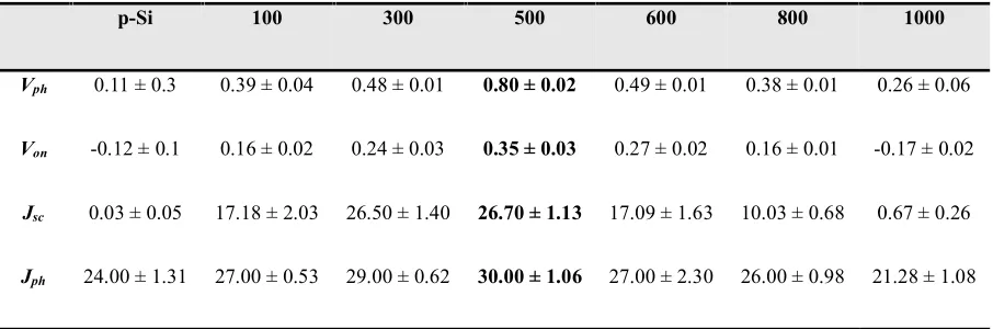
Table 1. Summary of Vph, Von, Jsc, and Jph of J-V characteristics as shown in Fig. 3.
p-Si 100 300 500 600 800 1000
Vph 0.11 ± 0.3 0.39 ± 0.04 0.48 ± 0.01 0.80 ± 0.02 0.49 ± 0.01 0.38 ± 0.01 0.26 ± 0.06
Von -0.12 ± 0.1 0.16 ± 0.02 0.24 ± 0.03 0.35 ± 0.03 0.27 ± 0.02 0.16 ± 0.01 -0.17 ± 0.02
Jsc 0.03 ± 0.05 17.18 ± 2.03 26.50 ± 1.40 26.70 ± 1.13 17.09 ± 1.63 10.03 ± 0.68 0.67 ± 0.26
Jph 24.00 ± 1.31 27.00 ± 0.53 29.00 ± 0.62 30.00 ± 1.06 27.00 ± 2.30 26.00 ± 0.98 21.28 ± 1.08
To understand the junction characteristics further, we carried out the Mott-Schottky
data. Vbi of the photocathodes can be estimated from the famous Mott-Schottky equation, where the intercepts of the straight lines yield 0.36 and 0.80 V at 200 kHz for 100- ALD cycle and
500- ALD-cycle photocathode, respectively. The slopes also indicate the photocathode of
p-type conductivity. Kenny et al. pointed out the catalyst layer thickness dependence on the MIS
junction characteristics utilizing partial screening charges and Debye length.43 Another report by Fujii et al. stated that the thickness of the deposited semiconducting layer on another
semiconductor of p-n heterojunction affects the depletion width, thus resulting in the Vbi variation.44 The change in the build-up of the depletion region at the p-Si/MoS2 (100- and 500-ALD cycles) interface junctions results in the increase of Vbi.
Figure 4. (a) Chronogalvanometry of our p-Si/SiOx/MoS2 photocathode under illumination with an applied bias of -0.3 V vs. RHE and (b) XRD patterns of the photocathode before and
after reaction.
Indeed, our p-Si/SiOx/MoS2 photocathodes regulated the overall energy barriers and impedances of the total junctions. Accordingly, the stable operation under 1 sun illumination
the secure chemical contact formed between the p-Si/MoS2 interface due to the ALD deposition method, which conformally deposited the layer on the silicon surfaces. Ding et al.
experimentally confirmed the effect of a higher quality interface for 1T-MoS2/Si by comparing the PEC characteristics of drop-casted 1T and CVD-grown 1T MoS2 films, showing improved performance with a 0.235 V vs. RHE onset potential for the CVD-grown MoS2 film on Si.45 The metallic nanojunctions in our mixed-phase (1T and 2H) MoS2 layers grown via ALD improved the stability for HER by reducing the contact resistance to Si. Upon stable operation
of the p-Si/SiOx/MoS2 photocathode for 70 h under the light, the resulting samples were analyzed by XRD as shown in Fig. 4b. The overall structures remained unchanged accordingly.
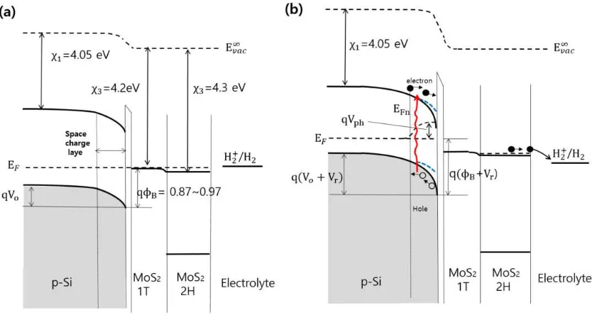
Figure 5. Energy band diagrams for energetically favorable exciton separation. (a) At
thermal equilibrium and (b) under illumination at reverse bias.
While the overall electronic structure of the photocathode can be depicted as a p-i-n
Schottky junction with p-Si. In Fig. 5, the band alignments of p-Si/SiOx/MoS2 and the electrolyte in the nanoscale domain are drawn to explain an injected electron transport path that
is energetically favorable, where Vo denotes the bend bending at 0 bias, Vr is the applied reverse
bias, 𝜙 is the Schottky barrier height, Vph is the photovoltage, EF is the Fermi level, and EFn is the quasi-Fermi level for electrons. For the band alignment at p-Si/MoS2 interface, all the necessary parameters in terms of vacuum level and normal hydrogen electrode level in
electrolyte of pH = 0.3 are shown in Fig. S1, where the p-Si doping level is ~1.6 x 1015 cm-3. The injected electron passes from 1T-MoS2 to 2H-MoS2, considering that 1T-MoS2 exhibits a work function of approximately 4.2 eV,46 which is not much different from that of the electron affinity of 2H MoS2 (4.3 eV), and higher electrical conductivity compared with the 2H phase.
Bai et al. studied the 1T/2H MoS2 contact with different contact types and concluded that the edge-contact model exhibits a low tunneling barrier of 0.1 eV and even Ohmic contact in the
case of having excess in-plane dangling bonds at the edge of 2H MoS247. An important interpretation from the J-V characteristics of the PEC performance is that the conditions for
bulk junction properties are fulfilled after 500 ALD cycles, and the MoS2 layer growth is already in the vertical direction. Therefore, in a situation of a high portion of 1T phase
with an ~10 cm density of Cl ions, within the 2H phase, there exists the 1T/2H MoS2 phase as an edge-contact type, indicating that this electron transfer path model is valid.
Since the non-ideal growth characteristic of our ALD MoS2 layers is well understood in the context of strong anisotropy in its covalency, the effects of active edge sites could be
correlated in PEC operations. The initial number of layers forms in a nanoflake-like structure,
mostly parallel to the substrate up to several tens of nm, followed by growing in the vertical
maintaining the electrochemical activation sites for the HERs. The amount of surface
recombination reduction leads to an increased Vph,48 as observed in our experiments. The quantitative analysis of the surface energetics can be understood using Eq. (1),22
= exp − = exp [− ] (1)
where 𝑛 is the surface electron concentration at light, 𝑛 is the surface electron
concentration at dark equilibrium, and 𝛾 is a constant at the interface, which is the ratio of
energy states to the bulk, and Vo is the amount of band bending at the junction interface. From Eq. (1), we can deduce that the MoS2 catalyst layer’s thickness range is in the nanoscale domain, changes the surface charge concentration (here, electrons) of the Si, and modifies the surface
energetics. The induced band bending also affects the photocurrent increment with the MoS2 layer thickness to the certain point, which can be analyzed using the Butler−Volmer relation in
Eq. (2).49
𝑖 =𝑖 [ exp ( ) - exp (− ( ) )] (2)
Here, 𝑖 is the electron current, 𝛼 is the electron charge transfer coefficient, and 𝜂 is the
overpotential. Based on the equation, the induced band bending modification explained above
is an influencing factor for the exchange current and for the overpotential, 𝜂. The current
induced within the bulk region is the sum of the current induced in the junction (depletion
region) and the current from the diffusion outside the depletion quasi-neutral region, which can
be expressed by Eq. (3),50
i = qI − 𝑞𝑛 , (3)
depletion region, and L is the bulk diffusion length of Si. Since the depletion region variation
was confirmed from the Mott-Schottky analysis in Fig. 3d, we can conclude that for a certain
MoS2 thickness, the solid junction characteristics between the Si and the MoS2 thin film play a role in enhancing the photocurrent. As a result, the spatially genuine 3D architectures (i.e.,
laterally homo and vertically heterojunction) with mixed-phases of 1T and 2H of MoS2 mainly offer synergetic functions in PEC HERs.
The ALD deposited MoS2 layers gradually alleviate the FLPss effect, and at the same time forming a bulk heterojunction interface.27 Considering the semiconductor p-n heterojunction utilized in PEC process, there are two types of Vph values. One is at the p-n junction interfaces, and the second is on the surfaces, which are MoS2/electrolyte interfaces.36 It is confirmed in our previous study that our MoS2 is insensitive to light (i.e., high doping concentrations). It is concluded that the driving potential for the generated electron-hole pair
separation is and p-n junction interface-dominated Vph. Now, considering the p-n heterojunction part in the p-Si/MoS2, the built-in potential can be expressed by conventional solid-state physics in Eq. (4),51
𝑞𝑉 = kTln + 𝜒 − 𝜒 + − 𝑘𝑇𝑙𝑛[ ] (4)
where 𝑉 is the built-in potential, T is the temperature (294 K), q is the charge of an electron
(1.6x 10 C), k is Boltzmann’s constant (1.38× 10 𝐽𝐾 ), 𝑁 is the acceptor
concentration of p-Si, 𝑁 is the donor concentration of MoS2, 𝜒 is the electron negativity for each type of semiconductor, EG for the band gap, 𝑁 and 𝑁 are the density of states of
𝜙 = + 𝜒 − 𝜙 (5)
where 𝜙 is the Schottky barrier height, 𝜙 is the work function of 1T-MoS2. The theoretical barrier height is therefore 0.87 to 0.97 V.
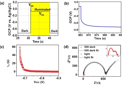
Figure 6. (a) OCP measurements of the 500 ALD-cycled MoS2/Si photocathode. (b) OCP decay after illumination for 20 min. The photocathode was illuminated at 100 mWcm-2 before measuring the OCP decay. (c) Carrier lifetime dependence on OCP of the photocathode. (d)
The OCP difference between dark and light directly indicates the Vph observed, the amount of the band bending of the junction interfaces (Fig. 6). Upon illumination, the amount
of the Fermi level shift (Vm) is 0.8 V by observing a very sharp increase in the OCP as shown Fig. 6a. This is distinctive in that typical PEC cells exhibit gradual increments when light turns
on. The subsequent saturation is attributed to the recombination at the electrode/electrolyte
interface, which results in 0.67 V (Vss). Considering the physical dimension of metallic 1T MoS2 of approximately 10 nm, which is much smaller than the depletion width, environmental Fermi level pinning (FLPnS) is expected by nano-Schottky junctions of p-Si/1T MoS2 although the surface states (FLPss) were passivated. Moreover, FLPnS competes with both FLDPox and FLDPox followed by pinch-off, enabling effective tuning of the Schottky barrier, which results in the final value of the effective barrier height of 0.8 V (Vm). By observing a sharp increase in OCP, indeed, fast transient behavior occurred when light turns on, implying that FLP is
negligible in the present electrochemical reactions. The OCP decay after turning off the light
provided information on the generated electron-hole pair recombination at the electrolyte
interface and the carrier lifetime as shown in Fig. 6b and c. The hole lifetime from the voltage
decay is given by Eq. (6).56
𝜏 = − (6)
Fig. 6b denotes the OCP voltage decay after 20 min of illumination and Fig. 6c shows the hole
lifetime determined from the results. The long lifetime of 60 s for the photocathode confirms
that the p-Si/SiOx/MoS2 structure effectively prevented surface recombination with the electrolyte. The fast charge transfer kinetics could be further understood by combining the EIS
measurements of our p-Si/SiOx/MoS2 photocathode shown in Fig. 6d. The charge transfer characteristics can be analyzed by means of an equivalent circuit model (Fig. S2b), and the
500-ALD-cycle photocathodes under dark and illumination are presented. The overall charge
transfer resistance was dramatically reduced under the illumination condition (red inserted)
compared to the dark equilibrium condition. Under illumination, for 500-ALD-cycle
photocathode, the charge transfer resistance (RMoS2) of 22.38 Ω·cm2 at the MoS2/electrolyte
interface and the p-Si/MoS2 junction resistance (Rjc) of 27.38 Ω·cm2 were obtained,
confirming the facile kinetics of the photocathode and are catalytically active. The Nyquist plot
shows the two distinctive semicircles, which represent the frequency-dependent
resistance-capacitance (RC) characteristics. The equivalent circuit, which is depicted in Supporting Fig.
S2b consists of constant phase elements coupled with the charge transfer resistance. Measured
parameters are summarized in Tale. S1. R refers to the charge transfer resistance at the p
-Si/MoS2 junction, R is the charge transfer resistance between the MoS2 and the
electrolyte, respectively. Note that under illumination, the R and R significantly
decreased more than an order of magnitude compared with that of the dark equilibrium
condition, which depicted the induced voltage drop across the. R , charge transfer
resistance can be derived from the impedance scan of the low-frequency range, the charge
transfer resistance at junction Rjc, and bulk resistance Rbulk from the mid-frequency range to high frequency. Qjc is the junction space charge region capacitance, and QMoS2 is the MoS2/electrolyte interface capacitance. The MoS2/electrolyte resistance was the lowest for the 300 ALD cycle photocathode, which is due to the vertical layers and exposure of the edge sites.
The resistance values for 500 ALD cycles photocathode are somewhat higher than those of the
300 ALD cycle photocathode. The second semicircle, which corresponds to the
capacitance-resistance (RC) through the p-i-n junction, indicates that the illumination increases the junction
voltage.
employing mixed-phase metal chalcogenides on Si for application in PEC water splitting. First
of all, the issues of FLPss could be cleared by ALD passivation. The other would be Fermi-level pinning (FLPnS) by nanoscale Schottky junctions (p-Si/1T MoS2).57 When it comes to the metallic 1T MoS2 contacted with Si, which forms the increased Schottky barrier height by environmental Fermi-level pinning. Moreover, it has trade-off effects by Fermi-level depinning
(FLDPox) by the presence of oxide interfaces, i.e., SiOx.58 We suspect that these mechanisms cancel out each other in Vph enhancements. Because of the discontinuous nature of the deposited layers (based on metallic 1T MoS2), electrical charges are screened only partially, inducing discontinuous junctions. This is also responsible for Vph increase although the junction properties are not the same as the bulk counterpart. Such a conclusion is plausible as studied
on the thickness dependence of catalyst layers on the junction characteristics, insisting that the
catalyst layer thinner than the Debye length only partially screen charges with nonideal
characteristics. Note that in such PEC systems, the currents flow not only through the nanoscale
Schottky (metal-semiconductor) junctions but also through semiconductor-electrolyte
interfaces. This differs from conventional solid-state devices and was systematically studied
by Rossi and Lewis.59 Therefore, pinch-off effects by Fermi-level depinning (FLDPinhm) operates from inhomogeneous Schottky junctions at the nanoscale.
Conclusion
Our chlorine-rich, ALD-grown MoS2 was deposited with different cycles on lightly doped p-Si. Neither a high-temperature sulfurization process nor any interface engineering was
necessary due to the mixed-phase characteristics of the MoS2 thin film. Thickness-dependent PEC characteristics were theoretically demonstrated along with experimental results. Our
30 mA·cm-2 and excellent stability (75hrs under 1 sun illumination). ALD-grown MoS2 film can induce energy band bending, resulting in a Vph enhancement, which coincides with a bulk
p-i-n junction model. The energetically favorable charge transfer mechanism is introduced for
the embedded metallic 1T phase MoS2.
Experimental section
Atomic layer deposition: Atomic layer deposition of the MoS2 films. The MoS2 film was grown
on a p-type silicon wafer (Boron doped, 1-30 Ωcm, 525±25 μm thickness) using a
custom-designed ALD system. The silicon wafer was cleaned with piranha solution, a 3:1 mixture of
concentrated sulfuric acid (H2SO4) with hydrogen peroxide (H2O2), for 20 min to remove any organic residues on the surface followed by immersion in buffered oxide etch or BOE
(HF:NH4F 7:1) to remove the native oxides. The chamber was heated and stabilized for 30 min before reactants were introduced. The MoS2 thin film was deposited at a temperature range of 250 - 300°C using MoCl5 (99.6%, Strem Chemicals, Inc.) and H2S (3.99%, balanced N2, JC Gas, Korea) and a carrier gas of Ar (5N, JC Gas, Korea). The pulse time was controlled to be
0.2 s followed by 15 s of purging with Ar at a gas flow of 50 sccm.
Material characterization: The morphology of the MoS2 film was observed by field-emission scanning electron microscopy (FESEM; JS7500F, JEOL, Japan). Cross-sectional images were
obtained by focus ion-beam etching (SMI305TB, SII, Japan), and high-resolution transmission
electron microscopy (HRTEM; JEM2100F, JEOL, Japan). Chemical compositions of the
surface were analyzed by X-ray photoelectron spectroscopy (XPS’ ESCA sigma Probe, Thermo
VG Scientific). MoS2 formation was characterized by Raman spectroscopy (RM1000 microprobe, Renishaw, United Kingdom). Structure analysis using energy-dispersive X-ray
Electrochemical characterization: All electrochemical measurements were performed using a
three-electrode system with Ag/AgCl as the reference electrode, a Pt wire (diameter of 0.5 mm)
as the counter electrode and MoS2 on a silicon substrate as the working electrode. Cyclic voltammetry and linear sweep voltamperometry were performed using a VMP3 Potentiostat
from Bio-Logic at a scan rate of 50 mV/s in 0.5 M of H2SO4 (pH 0.3) as the electrolyte. Electrochemical impedance spectra were measured over a frequency range of 106 to 0.1 Hz at 0 vs. the reversible hydrogen electrode (RHE). The Mott-Schottky impedance was performed
at 300 kHz to 1 kHz at a bias of -0.6 V to 0 V vs. RHE at 1 sun illumination. The electrode area
was 0.785 cm2. The Xenon light source (1 x 250 W, China) was calibrated to 1 sun irradiation. To make an ohmic contact, the back side of the silicon was scratched with a diamond cutter,
followed by a Gallium–Indium eutectic alloy and stuck to the copper electrode using silver
paste epoxy. Magnetic stirring at 500 rpm was performed during the experiment.
Acknowledgment
The authors acknowledge the grant by the Samsung Science & Technology Foundation
(SRFC-MA1502-09), and by the National Research Foundation of Korea
References
1 Sivula, K.; Krol, R. van de. Semiconducting materials for photoelectrochemical energy conversion. Nat. Rev. Mat. 2016, 1, 15010.
2 Xing, Z.; Ren, F.; Wu, H.; Wu, L.; Wang, X.; Wang, J.; Wan, D.; Zhang, G.; Jiang, C.; Sci.
Rep. Enhanced PEC performance of nanoporous Si photocathodes by converting HfO2 and
TiO2 passivaion layers. 2017, 7, 43901.
3 Hou, Y.; Abrams, B. L.; Vesborg, P. C. K.; Björketun, M. E.; Herbst, K.; Bech, L.; Setti, A. M.; Damsgaard, C. D.; Pedersen, T.; Hansen, O.; Rossmeisl, J.; Dahl, S.; Nørskov, J. K.; Chorkendorff, I. Bioinspired molecular co-catalysts bonded to a silicon photocathode for solar hydrogen evolution. Nat. Mater. 2011, 10, 434–438.
4 Choi, M. J.; Jung, J. Y.; Park, M. J.; Song, J. W.; Lee, J. H.; Bang, J. H. Long-term durable silicon photocathode protected by a thin Al2O3/SiOx layer for photoelectrochemical hydrogen evolution. J. Mater. Chem. A. 2014, 2, 2928-2933.
5 Zhao, Y.; Anderson, N. C.; Zhu, K.; Aguiar, J. A.; Seabold, J. A.; Lagemaat, J. V. D.; J. Oh. Oxidatively Stable Nanoporous Silicon Photocathodes with Enhanced Onset Voltage for Photoelectrochemical Proton Reduction. Nano Letters. 2015, 15, 2517-2525.
6 Feng, J.; Gong, M.; Kenney, M. J.; Wu, J. Z.; Zhang, B.; Li, Y.; Dai, H.Nickel-coated silicon photocathode for water splitting in alkaline electrolytes. Nano Res. 2015, 8, 1577-1583.
7 Wickramaratne, D.; Zahid, F.; Lake, R. K.Electronic and thermoelectric properties of
few-layer transition metal dichalcogenides. J. Chem. Phys. 2014, 140, 124710.
8 Wang, S.; Tian, H.; Ren, C.; Yu, J.; Sun, M. Electronic and optical properties of
heterostructures based on transition metal dichalcogenides and graphene-like zinc oxide. Sci. Rep. 2018, 8, 12009.
9 Lang, O.; Tomm, V.; Schlaf, R.; Pettenkofer, C.; Jaegermann, W. Single crystalline
GaSe/WeSe2 heterointerfaces grown by van der Waals epitaxy. ll. Junction
characterization. J. Appl. Phys. 1994, 75, 7814-7820.
10 Andoshe, D. M.; Jin, G.; Lee, C. S.; Kim, C.; Kwon, K. C.; Choi, S.; Sohn, W.; Moon, C.
W.; Lee, S. H.; Suh, J. M. Directly Assembeled 3D Molybdenum Disulfie on Silicon Wafer for Efficient Photoelectrochemical Water Reduction. Adv. Sustainable Syst. 2018, 2, 1700142-1700151.
11 Xiang, Q.; Yu, J.; Jaroniec, M.Synergetic effect of MoS2 and graphene as cocatalysts for enhanced photocatalytic H2 production activity of TiO2 nanoparticles. J. Am. Chem. Soc.
2012, 134, 6575-6578.
12 Chang, K.; Mei, Z.; Wang, T.; Kang, Q.; Ouyang, S.; Ye, J. MoS2/graphene cocatalyst for efficient photocatalytic H2 evolution under visible light irradiation. ACS nano. 2014, 8,
7078-7087.
13 Li, Y.; Wang, H.; Peng, S.Tunable Photodeposition of MoS2 onto a Composite of Reduced Graphene Oxide and CdS for Synergic Photocatalytic Hydrogen Generation. J. Phys. Chem. C. 2014, 118, 19842-19848.
14 Karunadasa, H. I.; Montalvo, E.; Sun, Y.; Majda, M.; Long, J. R.; Chang. C. J. A molecular MoS₂ edge site mimic for catalytic hydrogen generation. Science, 2012, 335, 698-702.
15 Li, Z.; Meng, X.; Zhang, Z. Recent Development on MoS 2 -based Photocatalysis: a Review.
J. Photochem. Photobiol. C: Photochem. Rev. 2017, 25, 39-55.
16 Hinnemann, B.; Moses, P. G.; Bonde, J.; Jørgensen, K. P.; Nielsen, J. H.; Horch, S.; Chorkendorff, I.; Nørskov, J. K. Biomimetic hydrogen evolution: MoS2 nanoparticles as catalyst for hydrogen evolution. J. Am. Chem. Soc. 2005, 127, 5308-5309.
17 Oh, S.; Kim, J. B.; Song, J. T.; Oh, J.; Kim, S.-H. Atomic layer deposited Molybdenum disulfide on Si photocathodes for highlyt efficient photoelectrochemical water redution reaction. J. Mater. Chem. A. 2017,5, 3304-3310.
18 Yin, Y.; Zhang, Y.; Gao, T.; Yao, T.; Zhang, X.; Han, J.; Wang, X.; Zhang, Z.; Xu, P.;
Zhang, P.; Cao, X.; Song, B.; Jin, S. Synergistic Phase and Disorder Engineering in 1T-MoSe2 Nanosheets for Enhanced Hydrogen Evolution Reaction. Adv. Mater. 2017, 29,
1700311-1700319.
19 Lukowski, M. A.; Daniel, A. S.; Meng, F.; Forticaux, A.; Li, L.; Jin, S.Enhanced
Hydrogen Evolution Catalysis from Chemically Exfoliated Metallic MoS2 Nanosheets J. Am. Chem. Soc. 2013, 135, 10274–10277.
20 Voiry, D.; Salehi, M.; Silva, R.; Fujita, T.; Chen, M.; Asefa, T.; Shenoy, V. B.; Eda, G.;
Chhowalla, M. Conducting MoS2 Nanosheets as Catalysts for Hydrogen Evolution Reaction. Nano Lett. 2013, 13, 6222-6227.
21 Hill, J. C.; Landers, A. T.; Switzer, J. A. Nat. Mater. 2015, 14, 1150-1155. 22 Thorne, J. E. ; Li, S.; Du, C.; Qin, G.; Wang, D. Energetics at the Surface of
Photoelectrodes and Its Influence on the Photoelectrochemical Properties. J. Phys.Chem.Lett. 2015, 6, 4083-4088.
23 Kwon, K. C.; Choi, S.; Hong, K.; Moon, C. W.; Shim, Y.-S.; Kim, D. H.; Kim, T.; Sohn, W.; Jeon, J.-M.; Lee, C.-H. Wafer-scale transferable molybdenum disulfide thin-film catalysts for photoelectrochemical hydrogen production. Energy. Environ. Sci. 2016, 9, 2240-2248.
24 Seo, J.; Kim, H. J.; Pekarek, R. T.; Rose, M. J.Hybrid Organic/Inorganic Band-Edge Modulation of p-Si(111) Photoelectrodes: Effects of R, Metal Oxide, and Pt on H2
GenerationEffects of R, Metal Oxide, and Pt on H2 Generation. J.Am. Chem. Soc. 2015,
137, 3173-3176.
26 Digdaya, I. A.; Adhyaksa, G. W.; Trześniewski, B. J. ; Garnett, E. C.; Smith, W. A. Interfacial engineering of metal-insulator-semiconductor junctions for efficient and stable photoelectrochemical water oxidation. Nat. Comm. 2017, 8, 15968-15976.
27 Fan, R.; Mao, J.; Yin, Z.; Jie, J.; Dong, W.; Fang, L.; Zheng, F.; Shen, M. Efficient and Stable Silicon Photocathodes Coated with Vertically Staning Nano-MoS2 Films for Soalr
hydrogen Production. ACS appl. Mater. interfaces 2017, 9, 6123-6129.
28 Lin, Y.; Battaglia, C.; Boccard, M.; Hettick, M.; Yu, Z.; Ballif, C.; Ager, J. W.; Javey, A. Amorphous Si thin film based photocathodes with high photovoltage for efficient hydrogen production. Nano.lett. 2013, 13, 5615-5618.
29 Ho, T. A.; Bae, C.; Lee, S.; Kim, M.; Montero-Moreno, J. M.; Park, J. H.; Shin, H. Edge-On MoS2 Thin Films by Atomic Layer Deposition for Understanding the Interplay
between the Active Area and Hydrogen Evolution Reaction. Chem.Mater. 2017, 29, 7604- 7614.
30 Joensen, P.; Crozier, E.; Alberding, N.; Frindt, R.A study of single-layer and restacked
MoS2 by X-ray diffraction and X-ray absorption spectroscopy. J. Phys. C: Solid State Phys. 1987, 20, 4043-4053.
31 Sim, U.; Yang, T.-Y.; Moon, J.; An, J.; Hwang, J.; Seo, J.-H.; Lee, J.; Kim, K. Y.; Lee, J.; Han, S. N-doped monolayer graphene catalyst on silicon photocathode for hydrogen production. Energy Environ. Sci. 2013, 6, 3658-3664.
32 Walter, M. G.; Warren, E. L.; McKone, J. R.; Boettcher, S. W.; Mi, Q.; Santori, E. A.; Lewis, N. S. Solar Water Splitting cells. Chem. Rev. 2010, 110, 6446-6473.
33 Esposito, D. V.; Levin, I.; Moffat, T. P.; Talin, A. A. H2 evolution at Si-based
metal-insulator-semiconductor photoelectrodes enhanced by inversion channel charge collection and H spillover. Nat. Mater. 2013, 12, 562-568.
34 Weitering, H. H.; Ettema, A. R. H. F.; Hibma, T. Surface states and Fermi-level pinning at epitaxial Pb/Si(111) surfaces. Phys. Rev. B. 1992, 45, 9126-9135.
35 Liu, D.; Li, L.; Gao, Y.; Wang, C.; Jiang, J.; Xiong, Y. The Nature of Photocatalytic “Water
Splitting” on Silicon Nanowires. Angew. Chem. Int.Ed. 2015, 54, 2980-2985.
36 Kronik, L.; Shapira, Y. Surface photovoltage phenomena: theory, experiment, and applications. Surf. Sci. Rep. 1999, 37, 1-206.
37 Benson, J.; Li, M.; Wang, S.; Wang, P.; Papakonstantinou, P. Electrocatalytic Hydrogen
Evolution Reaction on Edges of a Few Layer Molybdenum Disulfide Nanodots. ACS Appl. Mater. Interfaces, 2015, 7, 14113-14122.
38 Thorne, J. E.; Jang, J.W.; Liu, E.Y.; Wang, D.Understanding the origin of photoelectrode
performance enhancement by probing surface kinetics. Chem.Sci. 2016, 7, 3347-3354. 39 Quickenden, T.I.; Yim (née Tan), G.K. The relationship between open circuit photovoltage
40 Salvador, P.; Hidalgo, M. G.; Zaban, A.; Bisquert, J.Illumination intensity dependence of the photovoltage in nanostructured TiO2 dye-sensitized solar cells. J. Phys. Chem. B. 2005,
109, 15915-15926.
41 Liu, W.; Zhang, Y. Electrical characterization of TiO2/CH3NH3PbI3 heterojunction solar
cells. J. Mater. Chem. A, 2014, 2, 10244-10249.
42 Kirchartz, T.; Gong, W.; Hawks, S. A.; Agostinelli, T.; MacKenzie, R.C. I.; Yang, Y.;
Nelson, J.Sensitivity of the Mott–Schottky Analysis in Organic Solar Cells. J. Phys. Chem. C, 2012,116, 7672-7680.
43 Kenney, M. J.; Gong, M.; Li, Y.; Wu, J.Z.; Feng, J.; Lanza, M.; Dai, H. High-performance silicon photoanodes passivated with ultrathin nickel films for water oxidation. Science. 2013, 342, 836-840.
44 Fujii, K.; Ono, M.; Iwaki, Y.; Sato, K.; Ohkawa, K.; Yao, T.Photoelectrochemical
Properties of the p−n Junction in and near the Surface Depletion Region of n-Type GaN J. Phys. Chem. C. 2010, 114, 22727-22735.
45 Ding, Q.; Meng, F.; English, C. R.; Cabán-Acevedo, M.; Shearer, M.J.; Liang, D.; Daniel, A. S.; Hamers, R.J.; Jin, S. Efficient photoelectrochemical hydrogen generation using heterostructures of Si and chemically exfoliated metallic MoS2. J. Am. Chem. Soc. 2014,
136, 8504-8507.
46 Du, P.; Zhu, Y.; Zhang, J.; Xu, D. A.; Peng, W.; Zhang, G.; Zhang, F.; Fan, X. Metallic 1T phase MoS2 nanosheets as a highly efficient co-catalyst for the photocatalytic hydrogen
evolution of CdS nanorods. RSC Adv. 2016, 6, 74394-74399.
47 Bai, H.F.; Xu, L.C.; Di, M.Y.; Hao, L.Y.; Yang, Z.; Liu, R. P.; Li, X.Y. The intrinsic interface properties of the top and edge 1T/2H MoS2 contact: A first-principles study
J. Appl. Phys. 2018, 123, 095301-095306.
48 Reichman, J.The current‐voltage characteristics of semiconductor‐electrolyte junction photovoltaic cells. Appl. Phys. Lett. 1980, 36, 574-577.
49 Bard, A.; Faulkner, L. Electrochemical Methods. Fundamentals and Applications, 2nd edition. John Wiley and Sons 2001, New York, 2001.
50 Claeys, C. L.; Watanabe, M.; Rai-Choudhury, P.; Stallhofer, P. High Purity Silicon , The
Electrochemical Society, Inc, Burghausen, Germany, 2002.
51 Benchamekh, R.; Nesoklon, M.; Jancu, J.-M.; Voisin, P. Semiconductor Modeling
Techniques. Springer, Berlin, Heidelberg, 2012.
52 Schmidt, H.; Giustiniano, F.; Eda, G.Electronic transport properties of transition metal dichalcogenide field-effect devices: surface and interface effects. Chem. Soc. Rev. 2015, 44, 7715-7736.
53 Wang, H.; Zhang, C.; Rana, F. Ultrafast Dynamics of Defect-Assisted Electron–Hole Recombination in Monolayer MoS2. Nano Lett. 2015, 15, 339-345.
electronic structures of transition metal dichalcogenides: 2H-MX2 (M= Mo, W; X=S, Se,
Te) semiconductors. Physical Review B. 2012, 85, 033305-033310.
55 Hayden, T.; Dumesic, J.; Sherwood, R.; Baker, R. Direct Observation by Controlled Atmosphere Electron Microscopy of the Changes in Morphology of Molybdenum Oxide and Sulfide Supported on Alumina and Graphite. J.Catal. 1987, 105, 299-318.
56 Li, T.-L.; Lee, Y.-L.; Teng, H. High-performance quantum dot-sensitized solar cells based
on sensitization with CuInS2 quantum dots/CdS heterostructure. Energy. Environ. Sci. 2012, 5, 5315-5324.
57 Agrawal, A.; Lin, J.; Barth, M.; White, R.; Zheng, B.; Chopra, S.; Gupta, S.; Wang, K.; Gelatos, J.; Mohney, S. E.; Datta, S.Fermi level depinning and contact resistivity reduction using a reduced titania interlayer in n-silicon metal-insulator-semiconductor ohmic contactsn nanowire array electrode to construct a photocathode composed of elements abundant on the earth for hydrogen generation. Appl. Phys. Lett. 2014, 104, 112101-112105.
58 Smit, G. D. J.; Rogge, S.; Klapwijk, T. M. Scaling of nano-Schottky-diodes. Appl. Phys.
Lett. 2002, 81, 3852-3854.