mation Specification) is one of the most widely used methodology to model digital drivers as it satisfies the basic requirements of a behavioral model such as intellectual property protection, simple structure, fast simulation time and good accuracy.
As driver technology gets increasingly complicated and rise time of input signal gets increasingly smaller, important phenomenae such as simultaneous switching noise (SSN) becomes a major consideration when simulating multiple I/O drivers in the integrated circuit. Misrepresentation of noise might result in overestimation of signal strength and quality resulting in a high bit error rate and poor signal to noise ratio at the receiver end. This might lead to total failure of the system. With the size of the transistor shrinking, more and more I/Os can be accommodated on the chip, resulting in a greater probability of more drivers switching simultaneously, hence increasing the problems of SSN furthermore. Experiments show that IBIS models over-represents noise in the quiet line when placed in an environment where multiple drivers were present and switching simultaneously. A thorough analysis is performed to determine the inadequacies in IBIS with regards to SSN. A method is presented for compensating for the missing information by complimenting the IBIS model with a black box that is simulator independent, without compromising with the speed that IBIS enjoys over the transistor models.
by
Ambrish Kant Varma
A dissertation submitted to the Graduate Faculty of North Carolina State University
in partial fulfillment of the requirements for the Degree of
Doctor of Philosophy
Computer Engineering
Raleigh, NC
2007
Approved By:
Dr. Douglas W. Barlage Dr. Angus Kingon
Biography
gave me the strength to work through adversities and see the light at the end of the tunnel, even when the light was just a flicker of hope. Your confidence in me was nothing short of phenomenal - sometime it even surprised me. Every time I walked out of your room after a chat, I was in higher spirits, more determined and full with energy. I am glad you were an integral part of my graduate school experience.
I wish to thank Dr. Steer who helped me a lot in understanding this project and help me with anything that was required throughout the course of this project.
I also wish to thank Dr. Barlage and Dr. Kingon for giving constructive feedback on my work and helping me grow throughout these years.
I also wish to thank Ken Willis, C. Kumar, Lynne Green, Lance Wang, Shangli Wu, Hemant Kumar, Jilin Tan, Paul Musto and Ray Komow from Cadence, Bob Ross from Teraspeed and Michael Mirmak from Intel. There were a lot of great discussions, email exchanges, some intelligent and some dumb questions (all from my part of course). Thanks for everything.
My friends and colleagues who made this experience complete deserve special men-tion, Yongjin, Ravi, Lei, Monther, Karthik, Liang, Jian, Julie, Meeta, Shepp, Sonali, Jayesh, Krishnanshu, Evan just to name a few. Thanks a lot for your help, and the great time I had with you.
I also wish to express my appreciation for every member of my family. My parents provided me unconditional support throughout without which, this thesis might have been a Herculean task to finish.
I am grateful to God, who keeps bailing me out each time, everywhere.
Contents
List of Figures viii
List of Tables xiii
1 Introduction 1
1.1 The future of Signal Integrity . . . 1
1.2 I/O Buffer Modeling . . . 1
1.3 Motivation . . . 2
1.3.1 Noise . . . 2
1.3.2 High-Speed I-O Buffers . . . 3
1.4 Brief Overview of Research and Novel Claims . . . 3
1.5 Dissertation Outline . . . 4
1.6 Relevant Publications . . . 5
1.6.1 Journal Publications . . . 5
1.6.2 Conference Publications . . . 6
1.7 Abbreviations . . . 6
2 Review of State of the Art 9 2.1 Behavioral Modeling of I/O Drivers . . . 9
2.2 Issues with Behavioral Modeling . . . 10
2.2.1 Noise Issues . . . 10
2.2.2 Advanced Driver/Receiver Circuits . . . 12
2.3 IBIS (Input-Output Buffer Information Specification) . . . 14
2.3.1 Recent proposals to modify IBIS standard . . . 18
2.3.2 Inclusion of SSN Effects in IBIS models . . . 23
2.4 Parametric Macromodeling of I/O Buffers . . . 23
2.4.1 Temperature Dependence . . . 27
2.5 Spline Functions and Finite Time Difference Approximation . . . 27
2.6 Summary . . . 31
3 SPICE to IBIS, A Macro-modeling Tool to Develop IBIS Models 33 3.1 Introduction . . . 33
3.2 A Brief History of SPICE to IBIS . . . 34
4 Noise Issues with IBIS Models 41
4.1 Introduction . . . 41
4.2 Comparing SPICE and IBIS . . . 42
4.3 A Solution for better SSN Representation . . . 43
4.3.1 Simulation Results . . . 45
4.3.2 Challenges . . . 47
4.4 Summary . . . 47
5 Improving Behavioral I/O Buffer Modeling based on IBIS 48 5.1 Introduction . . . 48
5.2 IBIS Deficiencies . . . 49
5.2.1 Pre-Driver, Crossbar and Termination Currents . . . 50
5.2.2 Gate Modulation Effect . . . 51
5.3 Black-Box Modeling of Error Function . . . 53
5.3.1 Pre-Driver Current Error Correction . . . 55
5.3.2 Gate Modulation Effect Error Correction . . . 58
5.4 Achieving Improved Accuracy For System Level Simulations . . . 61
5.4.1 Circuit Implementation . . . 62
5.5 Metrics . . . 64
5.6 Test Results . . . 65
5.6.1 Same Equation for Rising and Falling Edges for Pre-Driver Current Error Correction . . . 67
5.6.2 Different Equations for Rising and Falling Edges for Pre-Driver Cur-rent Error Correction . . . 70
5.6.3 Different Equations for Rising and Falling Edges for Gate Modulation Effect Error Correction . . . 73
5.7 Results Analysis . . . 76
5.8 Summary . . . 83
6 Modeling of Voltage Mode Pre-Emphasis Driver in IBIS 84 6.1 Introduction . . . 84
6.2 Theory and Background . . . 85
6.2.1 Voltage Mode Pre-emphasis Driver . . . 86
6.2.2 Choice of Pre-Emphasis Driver . . . 87
6.3 IBIS Modeling Procedure . . . 87
6.3.1 Generation of Main and Boost Driver models . . . 87
6.3.2 Use of Driver Schedule to model Pre-emphasis Behavior . . . 89
6.4 Test Results . . . 91
6.4.1 Test Setup . . . 91
6.4.2 Analysis . . . 92
6.5 Issues and Challenges with IBIS modeling of Pre-emphasis Driver . . . 95
6.6 Summary . . . 95
7 System Level Validation of Improved Behavioral Model 96 7.1 Introduction . . . 96
7.2 Test Details . . . 97
7.3 IBIS Model and Black-Box Details . . . 97
7.4 Model Validation . . . 100
7.5 System Simulation and Results . . . 103
7.5.1 S-Parameter Package at power/ground, Ideal Transmission Line . . 103
7.5.2 S-Parameter Package at power/ground, Lossy Transmission Line . . 105
7.5.3 S-Parameter Package at Output, Power and Ground, Lossy Trans-mission Line . . . 105
7.6 SSN Simulation and Results . . . 108
7.6.1 Simulation Time . . . 108
7.7 Summary . . . 111
8 Conclusions and Future Work 112 8.1 Conclusions . . . 112
8.2 Contributions . . . 114
8.3 Future Work . . . 116
Bibliography 118
A MATLAB Code for generating Polynomials for VCCS 127
List of Figures
2.1 Simultaneous Switching Noise in an output driver . . . 11
2.2 Maximum Noise in a quiet line with increasing switching drivers (a) and increasing rise time (b) in a 1.8v system . . . 12
2.3 IBIS share in the SI/EDA industry (taken from [1]) . . . 13
2.4 Block Diagram of a CMOS buffer structure in IBIS . . . 15
2.5 IBIS Output Behavioral Model . . . 15
2.6 IBIS equivalent electrical Model from [2] . . . 16
2.7 Enhanced two Waveform Behavioral Model including Vdd-Vss Capacitance from [3] . . . 19
2.8 Quiet line output for SSN simulations with lumped package model. Green is transistor model, blue is normal IBIS and red is enhanced IBIS. (from [3]) . 20 2.9 Implementation of BIRD 95 from [4] (a) without Zvddq implementation and (b) with ZVddq . . . 21
2.10 Output voltage for rising edge in a 4 driver system with I Vs T table imple-mentation. Red curve is transistor model, green is IBIS, blue is IBIS with IT table and brown is IBIS with IT table and frequency dependent impedance, ZVDDQ . . . 22
2.11 Setup for generation of identification signals, from [5]. (a) setup for genera-tion of identificagenera-tion signal for sub models i1H and i1L(b) setup for generation of identification signals for weight coefficients w1H and w1L. . . 25
2.12 RC equivalent circuit for (d/dt)x(t) = (1/T)[v(t)−x2(t)],(T =RC), from [5] 26 2.13 Static (a) and Dynamic (b) representation for the Spline functions and Finite Time Difference Approximation modeling methodology. . . 29
2.14 Circuit representation of dynamic characteristics from [6] . . . 29
3.1 IBIS Output Behavioral Model . . . 35
3.2 S2IBIS tool flow . . . 35
3.3 Pullup (blue) and Pulldown (green) curve of an IBIS model created using S2IBIS3. . . 38
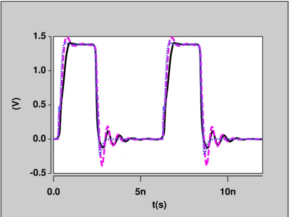
4.1 Test setup to compare circuits with IBIS and SPICE models for I/O drivers. 3 buffers are given simultaneously switching inputs and the 4th input is grounded to simulate quiet driver. . . 42 4.2 Output from the switching drivers. The response from IBIS modeled drivers
(dashed) does not capture SSN effects when compared to the transistor mod-eled driver (solid) . . . 43 4.3 IBIS (dashed) and Transistor (solid) model response in the quiet line (top)
and Pwr-gnd (bottom). . . 44 4.4 Placement of Voltage Controlled Capacitances (VCCAPs) in the circuit
de-scribed in fig. 4.1 . . . 44 4.5 Output from the switching drivers. The response from corrected IBIS drivers
(purple dashed) shows a better response than plain IBIS (blue dots) when compared to transistor modeled driver (solid) . . . 45 4.6 Quiet line output from the switching drivers. The response from corrected
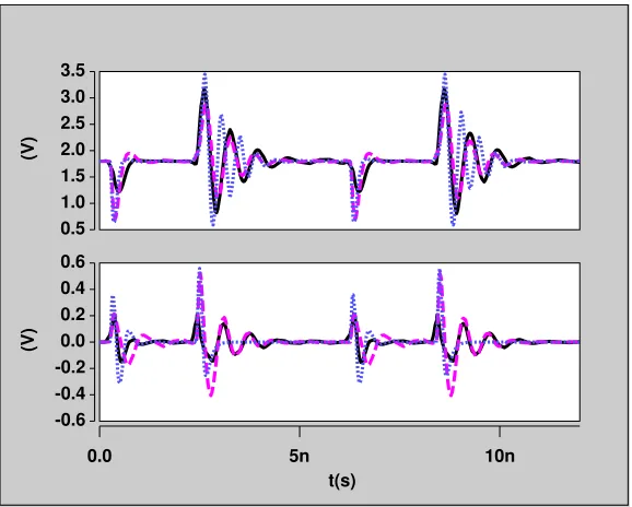
IBIS drivers (purple dashed) shows a better response than plain IBIS (blue dots) when compared to transistor modeled driver (solid) . . . 46 4.7 Power (top) and ground (bottom) response. The response from corrected
IBIS drivers (purple dashed) shows a better response than plain IBIS (blue dots) when compared to transistor modeled driver (solid) . . . 46 5.1 Tri-State Driver Schematic. . . 50 5.2 Rising edge current at the output pin of an I/O driver demonstrating the
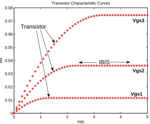
lack of pre-driver current in IBIS models (broken line) when compared to the transistor model (solid line). . . 51 5.3 Ids Vs VdsCharacteristic curves for NMOS transistors. While transistor level
models jump from one curve to the other with a change in Vgs, IBIS models confine to one curve (in this case, at Vgs2). . . 52 5.4 Effect of modulation of the gate voltage as a result of the power and ground
bounce. With the increase in number of drivers, SSN deteriorates, affecting the voltage response at the output pin in (a) transistor level models. Similar circuit does not elicit same response in circuits with IBIS level models (b). . 53 5.5 Black-box modeling approach. Breakdown of various components of the
pro-posed macro model (within the box with dashed lines), (left) and high level overview of the macro model with the IBIS element and the black-box (right). 54 5.6 (a) Power droop and ground bounce correlate with the switching of the buffer
. (b) There is a high correlation between the difference in current (solid line) at the Vdd pin between the transistor level model and the behavioral (IBIS) model and V(Pwr - Gnd) (broken line) of the IBIS model circuit. . . 55 5.7 (a) The correlation in fig. 5.6(b) is captured in a 2rd order polynomial that
When an edge is detected, the appropriate flag is raised, allowing the right circuit in fig. 5.10 to be used to simulate. . . 62 5.10 Circuits in black-box used to implement VCCS for (a) rising edge and (b)
falling edge. . . 63 5.11 Improvement in simulation accuracy is judged using area under the difference
curve of plain IBIS and transistor level models (top) and corrected IBIS and transistor level models (bottom). . . 64 5.12 Setup for testing the improved IBIS models. This setup shows lumped
par-asitic elements at both power and ground pins. . . 66 5.13 Voltage (top) and voltage difference (bottom) between plain IBIS and
transis-tor (blue dashed) and corrected IBIS and transistransis-tor (red dots) of a MICRON DDR2 Voltage mode driver, (a) with parasitics only on power pin and (b) parasitics on power and ground pin. The error correction is achieved with only one polynomial for both the edges. . . 68 5.14 Eye Diagrams comparing the corrected IBIS and SPICE transistor models
with only 1 polynomial for both edges in the black-box (top). Comparison of the plain IBIS and transistor models shows inaccurate IBIS curve (bottom) 69 5.15 Voltage (top) and voltage difference (bottom) waveforms at the output pin
of a cascading inverting driver (a) with only power pin parasitics in the test circuit and (b) with power and ground pin parasitics in the test circuit. The error correction used includes separate polynomial for the rising and falling edges. Plain IBIS (vout only) is denoted using blue dashed line, corrected IBIS (vout vccs) is shown as red dots and transistor model waveforms are shown as solid black lines. . . 71 5.16 (a): Vdd - Gnd voltage (top) and Vdd current (bottom) for test setup with
parasitics on both power and ground pins of a CMOS cascading inverting driver. (b): Quiet line voltage for the same setup. Plain IBIS is denoted using dashed line, the corrected IBIS is shown using dots and transistor model waveforms are shown as solid lines. . . 72 5.17 Voltage (top) and voltage difference (bottom) of a MICRON DDR2 Voltage
5.18 (a): Vdd - Gnd voltage (top) and Vdd current (bottom) for test setup with parasitics on both power and ground pins of a MICRON DDR2 driver. (b): Quiet line voltage for the same setup. Plain IBIS is denoted using dashed line, corrected IBIS is shown as dots and transistor model waveforms are shown as solid lines. Both error corrections are included in this figure. . . . 75 5.19 Percentage Improvement in Simulation Accuracy over plain IBIS models
(Area under the error curve) in (a) MICRON DDR2 and (b) Cascaded In-verter driver. . . 79 5.20 Percentage Improvement in Simulation Accuracy over plain IBIS models
(Mean Square Error)) in (a) MICRON DDR2 and (b) Cascaded Inverter driver. . . 80 5.21 Maximum noise in quiet line in (a) MICRON DDR2 and (b) Cascaded
In-verter driver. . . 81 5.22 Delay in the rising edge (relative % error) for (a) MICRON DDR2 and (b)
Cascaded Inverter driver. . . 82 6.1 Single Bit Response of an IBIS model of a voltage mode driver at the near
end (dot-dash line) and the far end of the lossy line (dash line). . . 85 6.2 Voltage Mode driver circuit with pre-emphasis (adapted from [7]). . . 86 6.3 Edge detection for FIR filter. Rising edge (left) and Falling edge (right). . . 87 6.4 IBIS model response without pre-emphasis to a 64 bit PRBS input sequence
at 2Gb/s. . . 88 6.5 Timing Diagram for Pre-emphasis implementation. Pre-emphasis is achieved
by combining the boost driver (scaled to be 50% of the main driver) to the main driver. The resulting signal is shown at the bottom. . . 89 6.6 Driver behavior without pre-emphasis (top) and with pre-emphasis (middle).
Input signal is also shown (bottom) . . . 91 6.7 Eye diagram simulation results for IBIS (a) and Transistor model (b) of a
pre-emphasis driver at the receiver input for a 64 bit PRBS input at 2Gb/s. 93 6.8 Simulation results for near and far end of the RC line with IBIS model (dashed
line) and transistor model (solid line) of VM pre-emphasis model. . . 94 7.1 Voltage (top) and current (bottom) of a MICRON DDR2 Voltage mode
driver, with s-parameter package model on the power pin. . . 98 7.2 (a): Vdd - Gnd voltage (top) and Vdd current (bottom) for test setup with
s-parameter parasitics on power pins of a MICRON DDR2 driver. (b): Quiet line voltage for the same setup. Plain IBIS is denoted using dashed line, while the corrected IBIS is shown as dots. Transistor model waveforms are shown as solid lines. . . 99 7.3 Test setup for IBIS model validation. . . 100 7.4 Validating the plain IBIS models (blue dashes) and the corrected IBIS model
middle) and transistor model (black, bottom). (b) Overlay of the 3 model outputs . . . 104 7.8 System simulation with power/ground package model, lossy transmission
line. (a) Eye diagram for output for plain IBIS (blue, top), improved IBIS (purple, middle) and transistor model (black, bottom). (b) Overlay of the 3 model outputs . . . 106 7.9 Same setup as fig. 7.8 except there is BGA package at output. (a) Eye
diagram for output for improved IBIS (purple, top), plain IBIS (blue, middle) and transistor model (black, bottom). (b) Overlay of the 3 model outputs. . 107 7.10 Setup for SSN simulation with BGA package at power and ground nodes. . 108 7.11 SSN Simulations with 4 drivers, 3 switching and 1 quiet. (a) Eye diagrams
for output for corrected IBIS (purple, top), plain IBIS (blue, middle) and transistor model (black). (b) Overlay of the 3 types of models. . . 109 7.12 Simulation time (total CPU time) for SSN simulation for plain IBIS,
List of Tables
3.1 S2IBIS2 Vs S2IBIS3 . . . 37 5.1 Percent Improvement in Simulation Accuracy over plain IBIS models (Area
Under Error Curve) . . . 77 5.2 Percent Improvement in Simulation Accuracy over plain IBIS models (Mean
Square Error) . . . 77 5.3 Maximum Noise (v) in the quiet line (Micron DDR2 SDRAM Driver) . . . 78 5.4 Maximum Noise (v) in the quiet line (Cascaded Inverter Driver) . . . 78 5.5 Absolute Delay (s) with respect to Input Signal (Micron DDR2 SDRAM
Driver) . . . 78 5.6 Absolute Delay (s) with respect to Input Signal (Cascaded Inverter Driver) 78 6.1 Simulation Time Comparison between IBIS and transistor model of
Chapter 1
Introduction
1.1
The future of Signal Integrity
The general trend in I/O signaling is to move towards serial I/Os to help achieve faster data transfer as well as an increase in bandwidth [8]. Fast 10Gb/s signal speed through the serial link brings a faster edge rate in through the chip [9]. With a faster edge rate, the otherwise transparent interconnects are not merely interconnects any more but behave more like a transmission line [10]. With transmission lines in the signal path, signal integrity issues such as timing, noise and electromagnetic interference are significant.Designers have to be aware of all the different ways they have to deal with such problems, specially when using behavioral models for I/O drivers.
1.2
I/O Buffer Modeling
Transistor-Level SPICE simulation of drivers and receivers are common in the Signal Integrity (SI) world, but more and more designers are looking for an alternative. The main reasons for this are:
• size of drivers and receivers; • time to complete simulations ;
These reasons have become common with multi-Gigahertz data rates, shrinking design cycles and tighter budgetary constraints, an overall design environment that has increasingly become more and more difficult in the last few years.
Perhaps the most important development in the field of SI analysis in the last decade or so was the development and consequently, the enhancements of behavioral mod-eling, most specifically, the Input Output Buffer information Specification (IBIS) standard. As driver and receiver circuitry became more complex, extracting the netlist from their IC design and then encrypting them became even more complex. With a number of sub-tleties involved in using the encrypted models along with the other board and/or system components, the task of simulation of the entire system for the purpose of signal integrity became complicated for the average PCB designer. IBIS provided a way to describe the necessary behavior of the I/O buffers in a text based table format that is easy to parse by simulators and hence fast. IBIS models, and in general, all behavioral models do not dis-close proprietary information and hence there is no need to encrypt them. Today, all good SI simulators have a capacity to simulate behavioral models as more and more designers demand their inclusion as part of the standard tools to simulate board level and system level designs. The International Technology Roadmap for Semiconductors (ITRS) predicts that due to their simplicity and speed of simulation, the behavioral modeling techniques will continue to be in demand in the near future, though they would have to be improved to describe the package and power and ground structures better [11].
1.3
Motivation
1.3.1 Noise
of backbone equipment. The trend has been to move to serial I/O standard (serial link) from parallel I/O standard (LVTTL) [14]. New data transfer standards such as SERDES (Serializer/Deserializer), LVDS (high speed differential) and others have been developed for error free transfer of data at these high bandwidths. With this shift, a similar shift in behavioral modeling methodology must be made, which will bring more complexities to behavioral modeling.
1.4
Brief Overview of Research and Novel Claims
The focus of this research is to be able to better understand how behavioral macro modeling works and then to come up with ways to improve upon the currently available technology.
The end result of this research would comprise of a system that would create accu-rate models that are not only good standalone but are equally useful in a large network that has multiple drivers switching simultaneously along with all the other parasitics involved. We would demonstrate novelty in these distinct areas of research:
• A key issue in behavioral models is the depiction of simultaneous switching noise
• Another reason for behavioral (IBIS) models to show discrepancies regarding SSN
is the fact that all the Voltage-Current (V/I) tables (used to model the pullup and pulldown devices) in the models are formed with a certain fixed value for the gate-source voltage of the active device. This voltage is a function of the power and ground voltage and should fluctuate with the power and ground voltage. While the circuits with transistor model of the I/O buffer reflects this phenomena, the circuits with IBIS models lack the effect. This effect is known as the Gate Modulation effect. It is imperative that there is a compensation that takes into consideration this effect and account for this variation in the system simulations.
• System level validation of the improved IBIS models will be done using a 512 Mb
DDR2 SDRAM from Micron Inc. Simultaneous Switching Noise (SSN) simulations will also be performed
• Another important consideration that is unique regarding this methodology is its
simplicity with respect to the other technologies without sacrificing accuracy. The black-box that is proposed in this work acts unobtrusively with the IBIS model without disturbing the circuit structure and physical aspects of the IBIS model.
1.5
Dissertation Outline
Chapter 2 is a review of the state of the art in behavioral modeling of input output buffers. It discusses the work of other groups in the academic world and the industry to improve the overall behavioral modeling scene. Some issues with behavioral modeling is also discussed in detail.
Chapter 3 discusses SPICE to IBIS (S2IBIS), a computer program written during the course of this research work. This program is used industry wide to make IBIS models using transistor netlists of I/O drivers. A brief discussion of how the various I/V and V/T curves are captured as text and organized and presented as tables in the model. All the IBIS models used for this research are made using S2IBIS (version 3).
Chapter 4 takes a look at noise in IBIS models. Simulation experiments are done to assess the effect of SSN on systems with IBIS models. It also details a preliminary solution to improve an IBIS model without modifying the model itself.
included.
Chapter 6 describes how S2IBIS (version 3) was used to make a voltage mode pre-emphasis I/O driver. The IBIS model is validated against the transistor level model of the voltage mode pre-emphasis driver.
In chapter 7, system validation of the improved behavioral model using S-Parameter model of a Ball Grid Array (BGA) package is performed. IBIS models of a DDR2 SDRAM I/O driver was used to perform the system tests. The IBIS model was constructed using the transistor model of the driver with the help of S2IBIS3. Details of the IBIS model as well as the black-box are provided in this chapter. Equivalent system level simulations were done with SPICE models of the driver to compare with the IBIS model results. Tests are performed in various modes starting with a simple point to point system without any package parasitics. More complex structures are added to this basic system to build up a complete system. IBIS and SPICE simulations are compared by observing the eye-diagram at each step of building this system.
Chapter 8 details how this work can be taken forward and concludes the disserta-tion.
The dissertation also includes the MATLAB scripts used in Chapter 4 to generate the black-box components as an appendix. Also included as an appendix is the IBIS model of a pre-emphasis driver as discussed in Chapter 6.
1.6
Relevant Publications
1.6.1 Journal Publications
• “Improving Behavioral I/O Buffer Modeling based on IBIS” Varma, A.; Steer, M.;
Franzon, P.; In preparation.
• “ Modeling and Validation of Voltage Mode Pre-Emphasis Driver in IBIS using S2IBIS3”
• “CAD Flows for Chip-Package Coverification” Varma A., Glaser A., Franzon P., IEEE
Transactions On Advanced Packaging, Vol. 28, No. 1, February 2005.
1.6.2 Conference Publications
• “Developing Improved I/O Buffer Behavioral Modeling Methodology Based on IBIS”
Varma, A.; Steer, M.; Franzon, P.; IEEE, Electrical Performance of Electronic Pack-aging, 2006, Oct. 23-25, 2006.
• “A New Method to Achieve Improved Accuracy with IBIS models” Varma, A.; Steer,
M.; Franzon, P.; IEEE, Electrical Performance of Electronic Packaging, 2005, Oct. 24-26, 2005.
• “Simultaneous Switching Noise in IBIS models” Varma, A.; Lipa, S.; Glaser, A.; Steer,
M.; Franzon, P.; International Symposium on Electromagnetic Compatibility, 2004. Volume 3, 9-13 Aug. 2004.
• “SSN issues with IBIS models” Varma, A.; Steer, M.; Franzon, P.; Electrical
Perfor-mance of Electronic Packaging, 25-27 Oct. 2004.
• “The development of a macro-modeling tool to develop IBIS models” Varma, A.;
Glaser, A.; Lipa, S.; Steer, M.; Franzon, P.; Electrical Performance of Electronic Packaging, 27-29 Oct. 2003.
1.7
Abbreviations
AMS Analog-Mixed Signal ANN Artificial Neural Network BGA Ball Grid Array
BIRD Buffer Issue Resolution Document CCCS Current Controlled Current Source CML Current Mode Logic
CMOS Complementary Metal-Oxide Semiconductor DAC Digital to Analog Converter
Gb/s Giga bits per second
HSTL High-Speed Transistor Logic or High-Speed Transceiver Logic IBIS Input Output Behavior Information Specification
ISI Inter Symbol Interference
ITRS International Technology Roadmap for Semiconductors LVDS Low Voltage Differential Signaling
LVTTL Low Voltage Transistor-Transistor Logic MSE Mean Square Error
NMOS Negative Metal Oxide Semiconductor PDN Power Distribution Network
PMOS Positive Metal Oxide Semiconductor PRBS Pseudo-Random Binary Sequence PWL Piecewise Linear
QDR Quad Data Rate
RBF Radial Basis Function RNN Recurrent Neural Network S2IBIS Spice to IBIS
SBF Sigmoidal Basis Function SERDES Serializer/Deserializer
SDRAM Synchronous Dynamic Random Access Memory SI Signal Integrity
SPICE Simulation Program with Integrated Circuit Emphasis SSN Simultaneous Switching Noise
SSO Simultaneous Switching Outputs SSTL Stub Series Terminated Logic
Tr Rise Time
Chapter 2
Review of State of the Art
2.1
Behavioral Modeling of I/O Drivers
Behavioral modeling of I/O buffers began in the early 1990s when simulating board level designs with huge transistor netlists started to become a time consuming and difficult task leading to the development of various vendor specific behavioral models that could simulate the buffers instead of requiring the spice netlists [16]. Because these were vendor specific and hence tool dependent models, a need for a common standard was felt. Engineers at Intel Inc. came up with a new method to model that was formatted in human readable, ASCII text format and invited Electronic Design Automation (EDA) vendors to make a standard that all designers can use, irrespective of the simulations tool they are using. This standard was known as Input Output Buffer Information Specification (IBIS, discussed in detail in section 2.3) and remains as the most dominant, if not the only standard that is being used widely to model I/O buffers behaviorally. The reason for this widespread use of IBIS could also be attributed to the S2IBIS (SPICE to IBIS) tool provided to the SI community by North Carolina State University [17] (discussed in chapter 3).
designers and model makers 1) Fast simulations, 2) IP protection and 3) Accuracy, making it a popular alternative to SPICE netlists, encrypted or otherwise.
Other methodologies have come to the forefront, specifically behavioral macro-modeling using parametric models [5, 19, 20, 21, 22, 23, 24, 25, 26, 27, 28, 29, 30, 31, 32] and behavioral macromodeling using spline functions and finite time difference approxi-mations [6], [33],[34] and [35]. Unlike IBIS, these modeling methodologies do not have a physical circuit based structure and use mathematical curve fitting techniques to construct a behavioral model. Both these methodologies are discussed in detail later in the chapter. Also noteworthy is the existence of VHDL-AMS and Verilog-AMS as languages to make behavioral models of I/O buffers but they are used more with IBIS than by themselves [36]. Also - VHDL-AMS and Verilog-AMS are new standards and there are a very limited number of simulators that can handle these languages as well as model makers that can make useful models using these languages [37]. log-AMS as languages to make behavioral models of I/O buffers but they are used more with IBIS than by themselves [36]. Also -VHDL-AMS and Verilog-AMS are new standards and there are a very limited number of simulators that can handle these languages as well as model makers that can make useful models using these languages [37].
2.2
Issues with Behavioral Modeling
2.2.1 Noise Issues
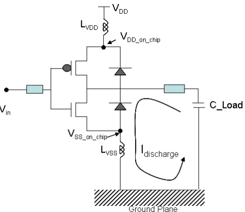
Faster devices with sub-nanosecond rise time and higher pin counts on the die results in more outputs switching together and faster. With a large number of devices switching, voltage glitches are induced due to an inductive voltage drop in each of the devices. As shown in fig. 2.1, switching causes the load capacitance to discharge itself causing stored charge to flow to the ground. This causes current surge in the power-ground loop, resulting in a reduced voltage available at the chip level (2.1) [38].
VDD on chip=VDD−L×(dIDD
dt ) (2.1)
where
Figure 2.1: Simultaneous Switching Noise in an output driver
Switching Noise, (SSN) or Simultaneous Switching Output (SSO) noise or Ground and Power bounce [39], [40],[41] .
The main issue of concern with SSN is the induction of substantial voltage in the quiet lines in the chip (drivers that are not switching), as shown in fig. 2.2, causing them to change state erroneously. Noise in the quiet line worsens with the increase in the numbers of switching drivers (fig. 2.2(a)) and the decrease in the rise time (fig. 2.2(b)) of the input signal. Hence with the faster devices and higher pins on the die, noise effects will get more pronounced.
With the increased usage of behavioral models of input output drivers in lieu of transistor models, it is important that accurate noise representation is made when a system simulation is performed with the behavior models. A lack of accurate noise analysis would result in an unrealistic simulation and might cause the entire system to fail after the chip is manufactured. A lack of accurate noise representation might also lead a designer to assume worst case scenario resulting in an over constrained design environment.
(a)
(b)
Figure 2.2: Maximum Noise in a quiet line with increasing switching drivers (a) and in-creasing rise time (b) in a 1.8v system
2.2.2 Advanced Driver/Receiver Circuits
as the received voltage, the common noise is rejected.
Driver-receiver technology has moved on from Low Voltage Transistor-Transistor Logic (LVTTL) technology to Emitter Coupled Logic (ECL) which, though an improvement on LVTTL being CML, still had issues like very high currents and negative power supply and then to Low Voltage Differential Signal (LVDS) which, as discussed above, was good for SI simulations and reduced power dissipation. Soon after LVDS came similar technologies like Low Voltage Power Emitter Coupled Logic (LVPECL) that has a larger differential voltage swing but less power efficient and Pseudo Current Mode Logic (PCML) that works on a higher power supply (3.3V) but using lower voltage swing allowing for faster switching and Hyper Transport Technology I/O that is an enhanced version of LVDS with a larger voltage swing. Similar advances have been made in high speed memory support and applications that interface with memory chips. The High Speed Transceiver Logic (HSTL) and Stub-Series Terminated Logic (SSTL) are new low-voltage I/O standards that are currently in use with memories such as Quad Data Rate (QDR) or Synchronous SRAM and DDR SDRAMs respectively.
With the move towards high-speed multi-gigabit serial transceiver links, also known as serializer-deserializer or SERDES [14], there will be a need to model advanced drivers that can perform transmitter or receiver side equalization such as driver side pre-emphasis or receiver side decision feedback equalization (DFE).
The increasing number of complex I/O signaling methods has made it harder for existing behavioral modeling methodologies to develop ways to model them. This has resulted in an increased use of transistor models and a decreased industry share of behavioral (IBIS) models, as shown in fig. 2.3. The main reason for this shift is shown in a survey in [1] which states that the increasing use of transistor models is because of unavailability of accurate behavior models of the advanced drivers. The survey also states that the users do not see transistor models as a long term solution to model high speed I/O drivers, and the sole reason for that is that the transistor models are too slow for system simulations.
2.3
IBIS (Input-Output Buffer Information Specification)
IBIS is the oldest and most widely used behavioral modeling technique. It has been made into an industry standard (EIA standard 656 -A). An IBIS model constitutes of a set of V-I tables that describe the static characteristics of the buffer and a set of V-T tables that represents the dynamic information of the buffer. These tables and other information is in a human readable text based format. A section of an IBIS model of an output driver is presented here:
...
[Model] driver Model_type Output
Polarity Non-Inverting
C_comp 5.00pF 5.00pF 5.00p
[Temperature Range] 27.00 100.00 0.0
[Voltage Range] 3.30V 3.00V 3.60V
[Pulldown]
|Voltage I(typ) I(min) I(max)
-3.30 -1.94A -1.61A -2.12A
-3.10 -1.78A -1.48A -1.94A
-2.90 -1.62A -1.35A -1.76A
-2.70 -1.46A -1.22A -1.59A
-2.50 -1.30A -1.10A -1.41A
-2.30 -1.14A -0.97A -1.23A
...
Fig. 2.4 shows the block diagram of a CMOS buffer. An IBIS model can be generated either
measure-Figure 2.4: Block Diagram of a CMOS buffer structure in IBIS
ment devices [47] or
2. by using the SPICE generated netlist running multiple SPICE simulations to get the necessary IV and VT table data.
Figure 2.5: IBIS Output Behavioral Model
The generation of IBIS models is facilitated by S2IBIS3 [17], a tool that runs multiple spice simulations to compile the IBIS model. Components of an output IBIS model is shown in fig. 2.5. SPICE to IBIS is discussed in detail in chapter 3.
These papers were written before most simulators started supporting the IBIS model and hence were used not just to understand how simulators interpret the IBIS model, but also let users convert the IBIS model to equivalent analog SPICE model that could be used in simulators that were not able to work with IBIS models. Most of the other IBIS related papers compare the performance of IBIS with SPICE. These comparisons vary from correla-tions of IBIS models with transistor level models [50] to complex issues such as the response of IBIS models to simultaneous switching noise (SSN) [42],[43] and [3].
Figure 2.6: IBIS equivalent electrical Model from [2]
Tehrani et al were the first to publish an approach to construct a SPICE behavioral model (fig. 2.6) from IBIS data that can be used directly in SPICE. The SPICE behavioral model consists of both static and dynamic information. The static information comes from the I-V tables in the IBIS models where as the dynamic data, that contains information about the switching of the devices, is from the V-T table in the model. The main equation in all the papers [2],[49] and [48] is of the output current Itotal given by:
The authors assumed that the switching coefficients α and β in the driver are related by the equation
α= 1−β (2.6)
where the argument provided by them was that in the beginning of a low to high transition, the total current is provided by the pulldown device and hence,α= 0 andβ = 1. Similarly, in the high to low transition,α= 1 andβ = 0. This relationship is not always true though, as both the pullup and pulldown devices don’t switch on or off simultaneously. For example, in the middle of a high to low curve, it is not necessary to have bothα = 0.5 and β = 0.5 as the NMOS transistor might be ‘less’ on than the PMOS transistor (or vice versa). The values ofα and β in this case are derived from one V-T table, hence to obtain both α and
β , the authors had to come up with another relationship betweenαandβ. Wang et al [48] remove this dependency and base their algorithm on two V-T curves. Hence they get two equations to calculateα and β.
In [47], Zak et al described in detail how to construct an IBIS model through mea-surements. They obtained an IBIS model of a Thin Quad Flat Pack (TQFP) bi-directional buffer and tested it against an IBIS model obtained through simulations. The authors reported good signal integrity results correlation between the 2 models.
A different comparison is done in an Altera white paper [51] where IBIS models for Stratix-II drivers for Altera and Virtex -4 drivers from Xilinx are compared against each other. Signal integrity tests are performed and comparisons for LVDS simulations at 1.3 Gbps and HSTL simulations at 600 Mbps are completed and compared against one another. As per their conclusions, Altera Stratix II FPGA buffers perform significantly better than the Xilinx buffers. In [52], a white paper from Mentor Graphics, the authors introduces new approaches for LVDS IBIS modeling and validates these models against transistor level models. They propose several ways to model the LVDS buffers under various loading conditions. Traditionally, LVDS buffers are modeled in IBIS by decoupling the 2 output terminals and dealing with each of them separately - assuming one terminal is equal in magnitude but opposite in polarity to the other terminal. This was done because IBIS was specifically designed for single ended buffers. In reality, though, both the LVDS outputs are not independent of each other as described by Tambone [53]. Hegazy et al in [52] describe a new way to model true differential buffers. This method is corroborated by Muranyi in [54].
2.3.1 Recent proposals to modify IBIS standard
Realizing the shortcomings of IBIS, particularly in the area of noise representation, many studies [3], [42], [43], [44] have been performed to improve upon the original IBIS. These studies and research are independent from the changes that the IBIS committee [55] makes to address other technological issues with IBIS. While some propose a solution that is added on to the IBIS models and does not need to change the way IBIS models are created, [42], [3], there are others that propose to overhaul the IBIS model itself [4], [45]. There is also a macromodeling methodology proposed by Telian et al at Cadence [1] that is not sufficient as is, but can be modified or added upon in the future to address signal integrity issues. In [56], Radhakrishnan realized that with rising edge rates, SSN/SSO would be a problem with IBIS models. He looks at the packaging as a possible area of improvement.
Unger [3] proposes an enhanced 2 waveform behavioral model that uses a new multiplier in the current equation. Recall that the total current in IBIS models is a function of the switching coefficients, α and β in eq. 2.3. He got better results when the above equations was changed to
power and ground rails shown in fig. 2.7. The results show a vast improvement in the correlation of the models with SPICE transistor level models (fig. 2.8). The downside to his implementation was that it required that the core IBIS equations in the simulator be changed. Before this could be proposed, many more tests have to be done and more exploration is needed. Even if the IBIS committee approves of the change, it would be up to the simulator companies to adopt the change in their IBIS element in the simulator.
Figure 2.7: Enhanced two Waveform Behavioral Model including Vdd-Vss Capacitance from [3]
Chen [42] proposed that SSO simulations with IBIS can be improved by adding Cdie that accounts for the on-chip power and ground capacitance. The inclusion of capacitance between the power and ground rail models the parasitics between the pullup and pulldown rail. This approach is similar in substance to the idea of a pre-stage capacitance proposed by Unger in [3].
BIRD 95
Figure 2.8: Quiet line output for SSN simulations with lumped package model. Green is transistor model, blue is normal IBIS and red is enhanced IBIS. (from [3])
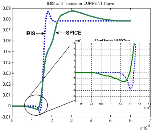
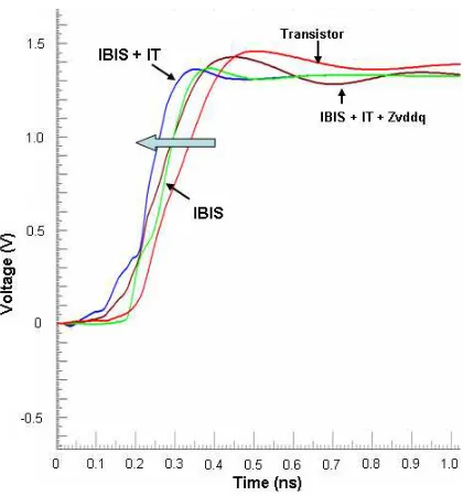
from either simulations or measurement of the transistor level model. This was proposed to the IBIS committee in the form of a Buffer Issue Resolution Document (BIRD) and was called BIRD 95. The idea behind a current Vs time (I Vs T) table in the IBIS model is that the simulator would calculate the total current that is flowing through the IBIS model provided when hooked up in a circuit, subtract it from the total current provided in the I Vs T table and then add the difference to the total current that flows through the IBIS model.
The main reason proposed was that the IBIS model does not include any predriver current information - hence it usually underestimates the current flowing in the actual driver. The proposal is summed up in fig. 2.9. In the figure, the I Vs T* is the difference in current that is added on to the IBIS model. In [15] good correlation is achieved using the I Vs T table along with a frequency-dependent impedance derived with the correct DC voltage applied at VDD pin and open-load condition. This impedance is named Zvddq by the authors and represents one portion of the on-die parasitics of the driver (fig. 2.9(b)). It is used in parallel with the I Vs T* current source in the circuit shown in the figure. Zvddq value is achieved by obtaining Z11 coefficients across the power and ground plain and achieving the impedance (L,C,R) values through it. Results achieved through only the I Vs T table implementation with current IBIS was not so satisfactory. Hence Zvddq plays an important role in making the IBIS model complete and better represented.
(a)
(b)
Figure 2.9: Implementation of BIRD 95 from [4] (a) without Zvddq implementation and (b) with ZVddq
Figure 2.10: Output voltage for rising edge in a 4 driver system with I Vs T table imple-mentation. Red curve is transistor model, green is IBIS, blue is IBIS with IT table and brown is IBIS with IT table and frequency dependent impedance, ZVDDQ
BIRD 97
Another BIRD that deals with the issue of an inadequate IBIS models as far as power and ground bounce is concerned is BIRD 97 [45]. An IBIS model has Voltage-Current (V-I) tables that are extracted for a single gate voltage inside the driver. With varying power/ground voltages due to noise, the gate voltage varies as well, hence producing a different characteristic curve for the device in the driver. While this effect is captured in HSPICE simulation of the driver netlist, the IBIS simulation solely depends on the one V-I table (pullup or pulldown) that is provided in the model. The higher the noise, the higher is the mismatching between IBIS and Spice results.
By taking measurements in noisy conditions, the V/I and V/T tables can retain the in-herent SSN voltage characteristics. When used in SSN simulations, they would produce valid SSN simulations. The main issue with this method is to create a realistic enough SSN situation with sufficient I/Os switching producing enough power supply fluctuations. Also, this method would be hard to implement if the IBIS model is obtained through simulations using transistor netlists and models. The method is discussed in the IBIS Modeling Cookbo
2.4
Parametric Macromodeling of I/O Buffers
In the last few years, there has been a multi-prong effort to come out with a better and more robust method of macromodeling complex I/O drivers. The main motive among these groups is to focus on a methodology that uses the black box approach that models the drivers without necessarily knowing what’s inside these drivers. The two groups that have done considerable work in this area are the EMC group at Politecnico di Torino in Italy1 and a group at the Packaging Research Center (PRC) at Georgia Tech2. Both
these groups divide the model into a static and a dynamic part. The static part of the model is obtained by applying a simple DC sweep at the output and observing the current there. This is very similar to how IBIS gets its static characteristics through the V/I table. The input is kept either high for rising characteristic or low for the falling characteristics. The differences in their modeling methodology are apparent only in the dynamic section of the model. The group at Italy started out with using Gaussian Radial Basis Functions (RBF)[24],[5], moving on to sigmoidal basis function [28], [29] which are more suitable for fitting the actual relations of the ports and are more simple and effective macromodels. In contrast, the group at Georgia Tech modeled the dynamic section of the model by using Finite Time Difference Approximations and then moved on to recurrent neural network to generate their models. The Georgia Tech approach is discussed in the next section. In this section, a brief study of how the Italian group (Stievano et al) came up with a new
1
http://www.emc.polito.it/
2
way to model drivers and receivers using parametric modes. Parametric values are derived by fitting a form of discrete-time models involving present and past samples of input and output variables [57], [31],[28],[29],[26],[24],[25],[5]. Here is a step by step analysis of their method.
1. The first step in this methodology is to characterize the circuit by its constitutive rela-tion. This is a relationship between the ports and should describe the output currents (for instance) as a function of all the voltages nodes in the model, for example as in [31] the authors describe this constitutive relation of the LVDS circuit as the a relation of the output current as a function of the common voltage (Vc) and the differential voltage (Vd) of the differential circuit. Another way to describe the constitutive rela-tion of the same circuit would be the relarela-tionship of the output current with respect to the output voltages. In [24], the authors describe the functional form of receiver to be modeled as a relation between not only the input port voltage and current but also the voltage and current of the power supply port. This is done because the model would carry additional information on the effects of the power supply noise and other electro-magnetic interference the receiver might experience.
Eq. 2.8 gives the constitutive relation for the LVDS driver with 2 output terminals. It can be observed that the output currents at each terminal is a function of both the terminal voltages.
i1=i1H(v1, v2)
i2=i2H(v1, v2)
and i1=i1L(v1, v2)
i2=i2L(v1, v2)
(2.8)
The output current for each terminal is divided between 2 sub models, one for the high logic state (H) and the other for the low logic state (L).
2. Combine high an low partial models (or sub models) by means of time-varying weight-ing coefficients w1H(t) and w1L(t) that accounts for the logic state transitions of the sub models and help the sub models inH and inL in transitioning from one state to the other.
i1 =w1H(t)∗i1H(v1, v2) +w1L(t)∗i1L(v1, v2)
i2 =w2H(t)∗i2H(v1, v2) +w2L(t)∗i2L(v1, v2)
as well. These two steps are together known as the process of model selection. 3. Obtain parametric relations of the sub models inH and inL by summing static and
dynamic effects.
i1H =i1H(static)(v1, v2) +i1H(dynamic)(v1, v2,dtd)
i2H =i2H(static)(v1, v2) +i2H(dynamic)(v1, v2,dtd)
(2.10)
(a)
(b)
Figure 2.11: Setup for generation of identification signals, from [5]. (a) setup for generation of identification signal for sub models i1H and i1L (b) setup for generation of identification signals for weight coefficients w1H and w1L.
signal as shown in fig. 2.11. These responses are representative of the driver that is being modeled. The estimation signals of a driver are obtained by exciting its output terminals with suitable voltage waveform. In the case of a differential driver, [31] the authors supply differential voltage on the 2 outputs. The output terminal currents are taken to be the static part of the above equation. This is done at a fixed logic state of either high or low with a DC sweep done at the output. For dynamic models, defined as sub models with static characteristics plus parametric correction (or sub models that includes separate dynamic information) [25], the dynamic parameters of the above equations are a little more complex to achieve. The estimation signals are the same as for the static case but with wide random steps (for non-linear parametric models) or pseudo-random bit sequence (for linear parametric models). These signals are obtained by recording i1(t) and i2(t) (at the output) when the driver is either
low or high and the voltage source at the output (refer fig. 2.11(a)) apply a staircase waveform. The parameters are estimated by fitting the estimation signals to an RBF representation.
The weight coefficients w1H and w1L are then estimated by applying a second set of identification signals. As shown in figure 2.11(b), the identification signals are the voltage and current responses during state transitions for 2 different load conditions. In [31] the authors describe the modeling of a differential driver and receiver circuit. The modeling of the receiver follows the same method as for the driver (discussed above). The authors note that the modeling process for receivers is relatively easier as compared to drivers, a fact also noted when creating IBIS models. Receiver models are only critical where clamping structures are present in the models.
Figure 2.12: RC equivalent circuit for (d/dt)x(t) = (1/T)[v(t)−x2(t)],(T =RC), from [5]
by either directly in a simulator or in another behavioral model that accepts Verilog or VHDL-AMS models such as IBIS [29],[31].
In [5], the authors model a multistage output buffer using the Radial Basis Func-tion (RBF) technique by drawing a relaFunc-tion between the driver output current and output voltage similar to equations in eq. 2.9.
In [30], Stievano et al perform system level simulations with the parametric macro-models and generate eye diagrams to show that the generated macromacro-models are accurate for system simulation even for long bit sequences.
2.4.1 Temperature Dependence
Stievano et al also discuss the role of temperature in modeling of I/O ports in [57] and [29] by including an extra variableT in their model selection step (1 and 2 above). An example of a model representation is
i(k;T) =w1(k;T)∗i1(k;T) +w1(k;T)∗i2(k, T) (2.11)
To derive the dependency of the parameters on T, the linear parameters of the sub models is estimated for several drivers at different temperatures. The authors find that the parameters dependence on T can be approximated by a piecewise linear function [29].
2.5
Spline Functions and Finite Time Difference
Approxima-tion
1. Non-Linear relation is drawn between driver output current and voltage.
io(k) =w1(k)f1(vo(k)) +w2(k)f2(vo(k)) (2.12)
2. In the above equation (eq. 2.12), f1 and f2 are sub models that relate the output
currents and voltages when driver is set high (f1) and low(f2). f1 and f2 have both
static and dynamic information in them. They can be represented as follows:
f1(vo(k)) =f s1(vo(k)) +f d1(vo(k))
f2(vo(k)) =f s2(vo(k)) +f d2(vo(k))
(2.13)
3. Static values can be obtained using DC sweep and using nth order cubic spline. For example a third order polynomial fit would look like:
f1(v) =a1vi3+b1vi2+c1vi+d1
f2(v) =a2vi3+b2vi2+c2vi+d2
(2.14)
where f1 is for input set to high and f2 is for input set to low. In fig. 2.13, it can be
observed that just the static solution would have left out a lot of important information from the model. The dynamic solution is obtained using the static method (spline) along with finite time difference approximation. Just one previous time instance is used in this example. The authors claim that more accuracy can be achieved with more number of previous time instances but, of course, increasing the computational time for calculation of the coefficients and hence reducing the essential charm of the macromodel.
4. Dynamic values for this modeling methodology are obtained by including the previous time instances of the driver output current using the formula.
f1(t)−f1(t−∆t)
∆t =
∆ioh ∆t =i
′
oh (2.15)
And then implementing it using the circuit shown in fig. 2.14
(a)
(b)
Figure 2.13: Static (a) and Dynamic (b) representation for the Spline functions and Finite Time Difference Approximation modeling methodology.
Figure 2.14: Circuit representation of dynamic characteristics from [6]
5. w1and w2 are used for transitioning from 1 logic state to the other. They are obtained
io(k) =w1(k)f1(vo(k)) +w2(k)f2(vo(k)) by using w1 w2 =
f1a f2a
f1b f2b
−1
ia
ib
(2.16)
6. Both the rising and falling currents that are obtained from this methodology are represented as PWL voltage source.
7. In the final step of this method, SPICE Macromodel is generated using Voltage Con-trolled Voltage Sources (VCVSs - E elements in HSPICE) and Current ConCon-trolled Current Source (CCCS - F elements in HSPICE).
• Static Characteristics can be represented using VCVS
• Dynamic Characteristics represented using state equations and consequently, a
circuit implementation is made to represent the state equations as shown in fig. 2.14 .
• Non-Linear relation between driver o/p current and voltage is now a sub circuit
as below:
.subckt driver1 out1 gnd ...
...
.ends (driver1)
In [35],[34] the authors also mention that the method of preparing behavioral level model using Spline and Finite Time Difference Approximation is good for simple drivers and is not good for complex transistor level models. This is because the current method could not capture the high non-linearity that is present in the driver. In the same paper [35], the authors propose a new method for creating behavioral models for highly-non-linear driver circuits. They call this method of modeling Artificial Neural Network (ANN). Using this method, they describe the two sub modelsf1 andf2using Recurrent Neural Network (RNN)
representing the weight w1 and w2 as PWL voltage source. Sub models for driver output,
power supply node and ground port are represented using voltage dependent voltage source and voltage dependent current source. This is very similar to their modeling methodology described in [6]. The only difference is that for RNN,f1andf2includes power supply voltage
and ground voltage instead of being a function of only the output voltage. A RNN network with 2 hidden neurons was required to model the driver output current for [35]. In [33], the authors report 5 hidden neurons and 2 previous time instances were used to produce the characteristics of the receiver input while 5 hidden neurons were used to model the static characteristics of the receiver output. A delay element is also used in the receiver output. Similarly, the driver output current can also be modeled for driver input LOW as reported in [35]. The Gatech method described in [33], [34], [6] and [35] is not intuitive enough for a SI engineer to make behavioral model out of circuit level design. Unlike an IBIS model that can be obtained with minimal knowledge about how to create the model using tools like S2IBIS3, using the spline with finite time difference approximations method and the recurring neural network is difficult, even though the results described in the above mentioned papers show satisfactory results with a variety of driver-receiver circuits.
2.6
Summary
After a thorough review of all the available methodologies, it can be concluded that there is a need for a better solution in this relatively new field of behavioral macromodeling of I/O drivers. With a clear prospect of more complex I/O buffers and systems in the future, it can be said that
1. A more comprehensive solution to I/O macromodeling is needed. One that uses the circuit structures of the drivers while keeping the behavioral model as a black-box for it to be fast and also to protect proprietary information.
2. A simple to use but accurate extraction methodology is required
environment, system level simulations need to be performed with the new macromodel and compare against the standard transistor models.
Chapter 3
SPICE to IBIS, A Macro-modeling
Tool to Develop IBIS Models
3.1
Introduction
As discussed in Chapter 2, behavioral modeling of input output (I/O) buffers is fast becoming popular with system level designers as well as chip designers. One of the most widely used behavioral modeling methodology is IBIS (Input/Output Buffer Information Specification) which is a standard1 in the industry to model I/O buffers. At the same time,
the popularity and use of transistor level models to design and simulate digital circuitry is time tested and widespread. To bridge the two worlds of system level design and simulation and circuit level design and simulation, SPICE to IBIS (S2IBIS) was written. Now in its third release, S2IBIS is a tool that uses a SPICE netlist of an I/O buffer and generates its IBIS model. The third version was developed as part of this dissertation.
An IBIS model constitutes of a set of VI tables that describe the static charac-teristics of the buffer and a set of VT tables that represents the dynamic information of the buffer. S2IBIS sets up multiple SPICE simulations that derive all the static and dy-namic characteristics of the model, collects the information, processes it and presents it in the prescribed IBIS format as set by the IBIS committee [55]. This chapter includes how the various voltage sweeps are setup as well as the other subtleties that are involved with S2IBIS. This chapter also covers S2IBIS3 - the latest addition to the S2IBIS tools family.
1
One of the major issues that concerns model developers is the non-convergence of a spice netlist during simulations for IBIS models. S2IBIS3 resolves this issue, allowing the model-ing engineer to choose the voltage range with which to sweep the device. S2IBIS3 conforms to IBIS version 3.2 with backward compatibility to all the previous versions and is more accurate and easy to use and modify than S2IBIS2.
3.2
A Brief History of SPICE to IBIS
In the early 1990s, when the focus of the electronics industry was shifting from the microwave to the digital realm, professors at North Carolina State University ([59]) got together to work on digital macromodeling. The first translator from SPICE to IBIS was a part of this effort. It was a pragmatic effort to help achieve a permanent behavioral modeling methodology. The instant adoption of this program as well as fast evolution of the IBIS standard prompted a revision of S2IBIS as well. This resulted in S2IBIS (version 2). S2IBIS2 was used by the industry for a long time but IBIS had move on at a considerable pace and models created using S2IBIS2 were found to be incomplete or inaccurate or both, thereby generating the need for the next generation of the SPICE to IBIS tool.
Researchers (Professors M.B. Steer, and P. D. Franzon and their students, A. Glaser and S. Lipa) at NCSU volunteered to write these tool as a freeware to serve the tool’s purpose of helping to develop IBIS models industry wide. S2IBIS has also been used as a seed for companies to modify for their own flavor of SPICE.
3.3
S2IBIS2
An IBIS model can be generated either 1) by measurement - which requires having a well-controlled environment and measurement devices [47] or 2) by using the SPICE generated transistor netlist running multiple SPICE simulations to get the necessary IV and VT table data.
Figure 3.1: IBIS Output Behavioral Model
Figure 3.2: S2IBIS tool flow
S2IBIS2 generates the required VI curves for the model. These are the pullup, pulldown, power clamp and ground clamp curves shown as current sources in fig. 3.1. It also generates the VT curves for all output models. These are the Rising Waveforms and the Falling Waveforms. To derive all these curves, S2IBIS2 makes multiple SPICE simulation runs with different settings and extracts the relevant information from the SPICE output. For each component that needs to be evaluated, the command file has a header that provides all the default values such as the temperature range, voltage range, all the reference values and the packaging details. The command file also provides the pin list which describes the pin and connects the pins to their models. The command file also describes each model specified in the pin list with the exception of the reserved model names POWER, GROUND and NC.
invoked. As soon as the SPICE output files are created, they are examined for any errors or aborts. If there are no errors, the VI and VT tables are extracted from their respective files and formatted according to the IBIS specification. The last step is to print the IBIS model into a file.
3.4
S2IBIS3
S2IBIS2 was written in C programmable language along with Lex and Yacc (for the purpose of parsing the command file). As such, different operating systems needed different versions of the tool. Moreover, S2IBIS2 could generate IBIS V2.1 or lower generation models only whereas IBIS itself had evolved to Version 3.2. As such, S2IBIS3 was developed. The programming language used to develop S2IBIS3 is Java which makes it a) easy to understand, b) platform independent and c) ideal for future enhancements. S2IBIS3 is also backward compatible to all versions of IBIS. A key feature that has been implemented in S2IBIS3 is the capability of handling convergence issues with HSPICE. Non-convergence occurs because the SPICE netlists are not accurate for the voltage range that they are swept with. If non convergence is detected, the user is asked to enter new sweep values for the beginning and the end of the sweep. SPICE is again run with the new values and if again faces non-convergence, comes back and asks for new values again. This procedure is repeated until SPICE converges or user aborts.
S2IBIS3 not only creates IBIS Version 3.2 compliant models (with support for keywords such as[Series Mosfet]), but also more accurate models as well. Most notable among the improvements was the correct implementation of the clamp subtraction algo-rithm. S2IBIS2 did not perform the algorithm correctly as it only performed it within power clamp and ground clamp specific ranges for pullup and pulldown respectively. S2IBIS3 subtracts the clamp current from the entire Vgnd to 2*Vcc range. This prevents double counting of clamp currents in the simulators.
S2IBIS3 also includes a few extra commands to give more control to the user. Key words such as [ExtSpiceCmd] was added to append external spice setup command to the spice simulation files. Also, the VI table code was modified to make sure 100 entries are present in the table to make the model more accurate.
GUI GUI hard to implement GUI next step Platform Dependence Platform dependent Platform independent
Programming Language C, Lex, Yacc Java
Convergence No solution for convergence Improved Convergence Command File Uses a command file Uses same command file
structure as s2ibis2 Accuracy VI tables inaccurate Accurate Data Points less data points more data points Simulator support HSPICE, SPECTRE HSPICE, SPECTRE, ELDO
model using S2IBIS3.
3.4.1 Pullup and Pulldown curves
Both the I/V tables (Pullup and pulldown curves) are derived for output and I/O models. Only pulldown curves are extracted for open-drain models while pullup curves are extracted for open source models. For both pullup and pulldown curves, S2IBIS3 connects an input voltage source and an output voltage source. The input voltage is set so the output tries to drive high (for the pullup curve) or low (for the pulldown curve). The output voltage is swept from (Vgnd - Vcc) to 2* Vcc using a DC sweep, and the output current at each output voltage is recorded at the pad (current going into the pad is considered positive in IBIS). No package information (R pin, L pin and C pin) is included in the DC sweep. Pulldown I/V data is referenced to ground while pullup I/V data is referenced to Vcc.
Vtable=Vcc−Voutput
S2IBIS3 performs these sweeps for all corners (Typical, Minimum and Maximum).
−2 −1 0 1 2 3 4
−0.4 −0.3 −0.2 −0.1 0 0.1 0.2 0.3
Voltage (v)
Current (A)
pullup pulldown
Figure 3.3: Pullup (blue) and Pulldown (green) curve of an IBIS model created using S2IBIS3.
3.4.2 Clamp curves
Power and ground clamp curves are derived for input models and the output models with enable inputs. To find the power and ground clamp curves for input models, S2IBIS3 attaches a voltage source to the associated pin and sweeps the voltage source. The current at each voltage point is recorded.
To find the clamp curves for the ‘output’ models with enable inputs, a voltage source is attached to the associated pin, the driver is disabled (using the voltage source attached to the enable pin), and the output voltage is swept. The resulting current at each voltage point is recorded. The sweep range for ground clamp curves is (Vgnd - Vcc) to (Vgnd + Vcc), and Vcc to 2*Vcc for power clamp.
3.4.3 Ramp rate
Ramp rates are derived for all output models and is obtained using the transient analysis. It is specified as a ratio of voltage change to time fraction (dV/dt).
3.4.4 Rising and Falling Waveform curves
0 0.5 1 1.5 2
x 10−9
−0.2 0 0.2 0.4 0.6 0.8 1 1.2 1.4 1.6 1.8 Time (s) Voltage (v)
Rising Waveform, R_fixture=50, V_fixture=0 Rising Waveform, R_fixture=50, V_fixture=1.8
(a)
0 0.5 1 1.5 2
x 10−9
0 0.2 0.4 0.6 0.8 1 1.2 1.4 1.6 1.8 2 Time (s) Voltage (v)
Falling Waveform, R_fixture=50, V_fixture=1.8 Falling Waveform, R_fixture=50, V_fixture=0
(b)
Figure 3.4: 2 rising (a) and 2 falling (b) curves of an IBIS model created using NCSU S2IBIS3.
waveforms are derived by having the driver drive 50 Ω high (Vcc). The other curve in fig. 3.4(a) and fig. 3.4(b) is derived by having the driver driver 50 Ω low (Gnd).
A variety of loads (R fixture) can be used in S2IBIS3 to obtain rising and falling waveforms as a total of 100 waveforms are allowed in the IBIS specification. Deriving rising and falling waveforms is similar to deriving ramp rates. Some designers and model makers use the [Ramp] data instead of the V/T curves (Rising and Falling Waveforms) as the ramp rate is sufficient for current mode logic (CML) (non-push/pull) drivers and eliminates charge storage and over-clocking issues. Also, the ramp rate is much simpler to adjust and correlate as it is linear.
S2IBIS3 is available for public download2. The program has been downloaded nearly 1000 times and is used in the chip design industry worldwide. An FAQ is also available to help setup, run and use the program3.
All IBIS models used in this dissertation (Pre-emphasis driver, DDR2 driver, CMOS Cascading Inverter driver) are created using the S2IBIS3 program. The IBIS model of a voltage mode pre-emphasis driver is attached as an appendix in this dissertation.
3.5
Summary
This chapter discussed the North Carolina State University’s S2IBIS tools that were written to convert SPICE transistor level netlists into IBIS models. Now in its third revision, S2IBIS can be held responsible for the widespread use of IBIS as a behavioral modeling methodology. A brief discussion on how data for the V/I and V/T tables are derived from numerous simulations is made. A comparison of S2IBIS2 and S2IBIS3 is also done. S2IBIS3 is used throughout the EDA industry worldwide and is used for constructing all the IBIS models used in this work.
2
Available at http://www.ece.ncsu.edu/erl/ibis/s2ibis3/s2ibis3.htm
3
Chapter 4
Noise Issues with IBIS Models
4.1
Introduction
This chapter investigates how well IBIS can model simultaneous switching noise (SSN), also known as ground bounce, or simultaneous switching output (SSO). SSN occurs because of voltage glitches induced due to an inductive voltage drop when I/O drivers switch simultaneously [41].
The experiments done to determine the usefulness of IBIS models for SSN simula-tions is followed by a preliminary method to accommodate SSN information in circuits that use IBIS models and improve the noise simulations that are done with the models. The solution involves placing voltage controlled capacitances at the power, ground and output nodes of the driver. Equivalent circuits with transistor netlists and IBIS drivers (with and without improvement) are compared for simultaneous switching noise.

![Figure 2.9: Implementation of BIRD 95 from [4] (a) without Zvddq implementation and(b) with ZVddq](https://thumb-us.123doks.com/thumbv2/123dok_us/1504802.1184225/35.595.217.434.110.487/figure-implementation-bird-zvddq-implementation-b-zvddq.webp)
![Figure 2.12: RC equivalent circuit for (d/dt)x(t) = (1/T)[v(t) − x2(t)], (T = RC), from [5]](https://thumb-us.123doks.com/thumbv2/123dok_us/1504802.1184225/40.595.237.428.553.648/figure-rc-equivalent-circuit-for-t-rc-from.webp)