Ultralarge-Scale System-on-Chip Architectures using Scan Test
Bandwidth Management
B . Anjaneyulu
Abstract:-
This paper shows a few systems utilized to determine issues surfacing while applying check transmission capacity administration to substantial modern multicore framework on-chip (SoC) plans with installed test information pressure. These plans posture critical difficulties to the channel administration plot, stream, furthermore, instruments. This paper presents a few test rationale designs that encourage preemptive test booking for SoC circuits with installed deterministic test-based test information pressure. The same arrangements permit proficient treatment of physical limitations in reasonable applications. At long last, cutting edge SoC test planning calculations are rearchitected as needs be by making arrangements for: 1) setting up time-compelling test setups; 2) streamlining of SoC stick parcels; 3) distribution of center level channels in view of sweep information volume; and 4) more adaptable center insightful utilization of programmed test hardware channel assets. A point by point contextual investigation is outlined thus with an assortment of trials enabling one to
figure out how to tradeoff distinctive designs and test-related variables.
I. INTRODUCTION
enhancing test interface engineering or control rationale while tending to steering and format requirements or progression of centers, booking test techniques and limiting force utilization.
Systems proposed endeavor to limit SoC test time. The coordinated plan of decreases the test time by improving committed TAMs and stick countaware test planning. Parcel exchanged systems on-chip can supplant devoted TAMs in testing of SoC by conveying test information through an on-chip correspondence framework.
There are methods tending to synergistically TAM and wrapper configuration and test information pressure. Indeed, test pressure is currently getting to be an essential piece of SoC-based design for-test (DFT) plans. For instance, the approach of encodes tests for each center independently through linear feedback shift register (LFSR) reseeding with time-multiplexed automatic test equipment (ATE) channels conveying information to progressive centers. Correspondingly, a plan of uses static reseeding to test SoCs, where all centers share a solitary LFSR. The XOR test rationale performs pressure, which additionally manages a TAM configuration process.
ATE channel data transfer capacity administration for SoC outlines can assume a key part in expanding test information pressure with
no obvious effect on test application time. The approach displayed incorporates: 1) a solver equipped for utilizing info and yield channels progressively; 2) test booking calculations; and 3) TAM configuration conspires, all formulated for the embedded deterministic test (EDT) condition.
It is expected that all centers in the SoC are either heterogeneous modules, or wrapped testable units, and they come with their individual EDT-based pressure rationale, which is in this way interfaced with ATE through an enhanced number of channels. Therefore, test booking and TAMs can dole out a small amount of the ATE interface ability to each center. It expands pressure proportions and permits tradeoffs between the test application time, volume of test information, test stick check, and interface outline many-sided quality. The plan of is appropriate to any SoC-based test information lessening plan equipped for working with a differing number of In and yield channels.
it is difficult to decide the ideal portion of pins to centers for the best pressure. Moreover, since a specific center can be reused in various plans, an ideal number of channel pins for this center when inserted in one configuration may negate test reuse in different outlines. Under such conditions, the chip integrators gather information for all person centers, look at the information alongside all requirements for the plan, and after that physically decide test plans. This may bring about imperfect test information volume and bargained test application time, particularly in light of some anomaly squares having vast example tallies (PCs).
Transfer speed administration mitigates the reliance of center channels on the quantity of accessible chip-level pins, permits programmed booking of tests by making it straightforward to the clients, and fundamentally enhances test arranging at the corelevel. It additionally parleys the sharing of the chip-level channel pins, in this manner ensuring the best information volume and test time diminishments for the general plan. In this paper, we show a transfer speed administration plot for progressive outlines that lets a fashioner tradeoff settled and adaptable channel allotments per center and in addition physical requirements to limit the directing overhead of the TAM-based systems. Moreover,
a few strategies to convey the control information amid test are inspected through and through with another planning calculation that permits changing the In and yield channel distributions when exchanging the channel setups.
The rest of this paper is sorted out as takes after. After reviewing standards of the EDT-based transmission capacity administration in Section II, Section III depicts financially savvy plans utilized to convey control information, and in this way to setup SoC test arrangements. Segment IV presents a contingent blending based test scheduler. It makes ready for further developed test time decrease methods in light of adjusted I/O pins parceling, need based directing, and specific altering of interface throughput. Area V subtle elements test comes about acquired for this plan. This paper closes with Section VI.
II. PRIVIOUS WORK
given center k is signified as Ck ) in light of the control information delivered by a test scheduler. Since the output steering ways from the chip-level test pins to the center chip-level test pins are powerfully chosen by designs, this interconnection arrange is likewise alluded to as a dynamic scan router (DSR). Indistinguishable modules may have a similar test information in the communicate mode. Notwithstanding individual EDT decompressors, each center highlights X-veiling rationale securing its reaction compactor against obscure states and associating the center with a yield exchanging system. This system permits the packed yield streams from progressive centers to achieve a yield channel I (OCi ), and to be sent back to the ATE. So as to encourage test design reuse, test wrappers seclude all centers with the goal that they are free of each other.
As appeared in Fig. 1, the In DSR comprises of demultiplexers whose number matches the quantity of ATE In channels. Given a gathering of test designs, each demultiplexer associates the comparing channel to one of a few goal centers, as demonstrated by the substance of address enroll. The quantity of ATE In channels can't be littler than the limit of the biggest single center regarding its EDT In. Unmistakably, in the
assuming the worst possible scenario, we can at present test the biggest centers, each one in turn.
Fig. 1. SoC test environment with on-chip compression.
entryway In, assuming any) are associated with the demultiplexers such that n EDT In of guaranteed center are connected with n diverse ATE In channels, and each ATE channel serves roughly a similar number of centers.
This strategy yields the genuine size of the In demultiplexers and their control registers. Some last changes inside a solitary module are additionally conceivable to streamline the resultant DSR design what's more, stay away from exorbitant and long associations.
The yield DSR (Fig. 1) interfaces all center yields with the ATE by decreasing the quantity of test reaction streams so that they fit into the quantity of yield ATE channels. It is made up of various multiplexers to such an extent that every multiplexer serves to interface a few centers with an assigned ATE yield channel. Once more, the address registers determine which centers are to be watched for a given gathering of test designs. The yield channel mapping is done in a way like that of the In DSR. Note that all center yields include a client characterized fan-out keeping in mind the end goal to expand adaptability of choosing perception guides associated toward the multiplexers. It is additionally accepted that all center yields should be watched when tried.
It is significant that an adaptable utilization of ATE channels comes about in expanded pressure and raised encoding proficiency. Also, testing many centers in parallel by progressively apportioning ATE directs to various centers as per their necessities may abbreviate test application time. At long last, having individual decompressors running in proper vacancies makes it simpler to lessen the quantity of outer channels contrasted and the aggregate number of EDT In included by all centers together. In planning for the real test session, the following advances are done (an itemized depiction of this methodology can be found).
1) For each center, automatic test pattern generation (ATPG)- delivered test shapes are passed to a solver that unions furthermore, encodes them to touch base with last compacted test designs; moreover, the solver decides the negligible number of EDT In channels expected to pack guaranteed test design.
3) All test designs are bunched to shape gatherings (classes) of examples having indistinguishable both In channels and perception focuses.
4) Upon culmination of the above operations for each center, all classes are finished to a test scheduler; given design of both test get to systems and different imperatives (ATE channels, DSR engineering, control utilization, furthermore, others), it yields the last allotment of ATE In/yield channels to chose centers while applying progressive test designs.
Given both DSRs, one would now be able to plan use of test designs. Each test design t is portrayed by its descriptor including module m that will be practiced while applying test t, and the channel limit c, i.e., the quantity of EDT In what's more, yields required for this reason. All test designs having a similar descriptor frame a setup class x spoke to by its PC P(x). Each setup class can be part into different fragments with the end goal that test designs from a similar class are connected in disjoint time interims. The capacity to acquire a class may enhance the ATE channel usage, abbreviate the aggregate test time, and lessen the volume of control information.
III. CONTROL DATA DELIVERY
The approach outlined in Section II does not make any particular arrangements for the way control information is conveyed to SoC test rationale keeping in mind the end goal to setup test designs. It shows up, in any case, that the quantity of test setups, and henceforth the measure of control information one needs to utilize and exchange between the ATE and DSR address registers, may noticeably affect test booking and the resultant test time. Therefore, we start this paper by breaking down three option plans that can be utilized to transfer control bits and show how they decide the last SoC test rationale engineering.
A. Utilizing IJTAG
little, one can utilize it to convey the control information, as appeared in Fig. 2.
Fig. 2. Using IJTAG network to transfer control data.
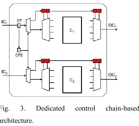
Fig. 3. Dedicated control chain-based architecture.
The upside of utilizing the IJTAG system to convey the DSR control information is a basic and simple approach to execute stream as the
system is every now and again used to set the centers TDRs. Notwithstanding, such an approach can just help a predetermined number of designs. This is on account of the IJTAG move clock is commonly 10 to 20 times slower than the sweep move clock. Conveying an extensive volume of control information can acquire an unsatisfactory add up to test time overhead. Thus, this design can be utilized for a generally modest number of test arrangements. In the event that the TDRs work with parallel refresh registers and numerous designs utilize a similar setup, a low throughput IJTAG control can be alleviated. On the off chance that one changes the control state Or maybe from time to time, the following design vector can be moved in coincidently with use of test designs, trailed by refreshing TDR when prepared to change to the new arrangement. It requires more DFT rationale, however.
B. Using Pipelines
amidst test information moving. The shadow registers are refreshed toward the finish of each example transfer. In this way, when a test design dispatches another test arrangement, the comparing control information should be stacked with its forerunner. Unmistakably, the main vector is solely a setup one.
The design of Fig. 4 underpins the same number of test designs as required. Be that as it may, the control information is constantly transferred through the ATE channels as a basic piece of a test vector. Thus, given a test design, a similar control information is rehashed for all test designs. The measure of control information is little, however, as the quantity of control bits per channel is ordinarily a small part of the test design move cycles.
Fig. 4. Pipeline architecture.
IV. TEST TIME REDUCTION
The analyzer transfer speed administration in display substantial SoC outlines and future kilo-center models with impressive decent variety in the outline styles and test needs of person modules requires arrangements past the abilities of stateof- the-craftsmanship DFT plans. Specifically, a test plan will have to progressively adjust to particulars of a given SoC engineering to guarantee an ideal usage of its interface transfer speed.
In this area, we recognize the key purposes behind existing arrangements' powerlessness to additionally decrease test application time and exhibit how rearchitecting a test scheduler and DSR systems can relieve it. At long last, we indicate how these strategies decrease the test time in a worldwide data transmission administration plot.
RTL Schematic
Technologycal schematic
Design summary
Simulation
VI. CONCLUSION
As Moore's law keeps on giving littler gadgets, outlines with a scope of center tallies, ability per center, and vitality per center have an emotional effect on SoC outline and test methodology. As appeared in this paper, the I/O assets given by an analyzer can be powerfully assigned to chose centers, though the aggregate number of diverts being used may remain unaltered. This worldview plainly calls for productive plans limiting the general test application time, while taking into account physical limitations, specifically, SoC stick allotments.
outline multifaceted nature of the TAM, and test application time.
REFERENCES
[1] K. Chakrabarty, “Test scheduling for core-based systems using mixedinteger linear programming,” IEEE Trans. Comput.-Aided Design Integr. Circuits Syst., vol. 19, no. 10, pp. 1163–1174, Oct. 2000.
[2] K. Chakrabarty, V. Iyengar, and M. D. Krasniewski, “Test planning for modular testing of hierarchical SOCs,” IEEE Trans. Comput.-Aided Design Integr. Circuits Syst., vol. 24, no. 3, pp. 435–448, Mar. 2005.
[3] A. Chandra and K. Chakrabarty, “A unified approach to reduce SOC test data volume, scan power and testing time,” IEEE Trans. Comput.-Aided Design Integr. Circuits Syst., vol. 22, no. 3, pp. 352–362, Mar. 2003.
[4] S. K. Goel and E. J. Marinissen, “Effective and efficient test architecture design for SOCs,” in Proc. Int. Test Conf. (ITC), 2002, pp. 529– 538.
[5] S. K. Goel, E. J. Marinissen, A. Sehgal, and K. Chakrabarty, “Testing of SoCs with hierarchical cores: Common fallacies, test access optimization, and test scheduling,” IEEE Trans. Comput., vol. 58, no. 3, pp. 409–423, Mar. 2009.
[6] P. T. Gonciari and B. M. Al-Hashimi, “A compression-driven test access mechanism design approach,” in Proc. 9th IEEE Eur. Test Symp. (ETS), May 2004, pp. 100–105.
[7] Y. Huang et al., “Optimal core wrapper width selection and SOC test scheduling based on 3-D bin packing algorithm,” in Proc. Int. Test Conf. (ITC), 2002, pp. 74–82.
[8] V. Iyengar and K. Chakrabarty, “System-on-a-chip test scheduling with precedence relationships, preemption, and power constraints,” IEEE Trans. Comput.-Aided Design Integr. Circuits Syst., vol. 21, no. 9, pp. 1088– 1094, Sep. 2002.