Volume 2006, Article ID 43917, Pages1–8 DOI 10.1155/WCN/2006/43917
Transceiver Design for Multiband OFDM UWB
D. M. W. Leenaerts
Philips Research, 5656 AE, Eindhoven, The Netherlands
Received 14 October 2005; Accepted 9 January 2006
Ultra-wideband (UWB) is an emerging broadband wireless technology enabling data rates up to 480 Mbps. This paper provides an overview of recent design approaches for several circuit functions that are required for the implementation of multiband OFDM UWB transceivers. A number of transceiver and synthesizer architectures that have been proposed in literature will be reviewed. Although the technology focus will be on CMOS, also some design techniques implemented in BiCMOS technologies will be presented.
Copyright © 2006 D. M. W. Leenaerts. This is an open access article distributed under the Creative Commons Attribution License, which permits unrestricted use, distribution, and reproduction in any medium, provided the original work is properly cited.
1. INTRODUCTION
Short-range communication systems (so-called wireless per-sonal area network (WPAN) systems) with ranges of up to 10 m are becoming popular in replacing cables and in en-abling new consumer applications. Examples such as Blue-tooth and ZigBee, which operate in the 2.4 GHz ISM band, have however a limited data rate, typically about 1 Mbps, which is insufficient for many applications like fast transfer of large files (e.g., wireless USB) and high-quality video stream-ing. In order to increase the data rate to several hundreds of Mbps, a higher bandwidth is preferred over a larger SNR. This became possible at the moment the FCC released spec-trum for UWB in the US spanning from 3.1 to 10.6 GHz with an average transmit power level of only −41.3 dBm/MHz [1,2]. Several proposals have since then been presented to realize a short-range high data rate communication link. At present, both direct-sequence impulse communication and multiband OFDM UWB systems are under consideration as a standard.
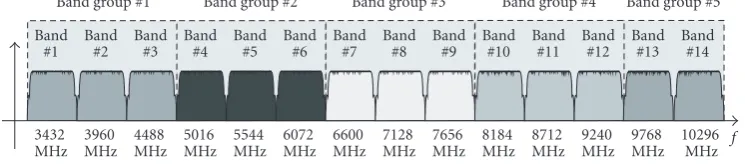
The standard proposed by the multiband OFDM alliance (MBOA) is based on subdivision of the large available band-width in subbands of 528 MHz (seeFigure 1) [2]. The data is QPSK-OFDM modulated on 128 subcarriers. Various modes are defined with data rates up to 480 Mbps. In the mandatory mode of operation (Mode 1), a frequency-hopping scheme in the three lower bands is implemented. Using only the three lower bands allows the use of a bandpass prefilter to reduce the interferer level of the 5 GHz ISM band. After each symbol period of 312.5 ns, a 9.5 ns guard time is available for hop-ping to the next band.
This paper intends to give an overview of the current sta-tus in multiband OFDM-based UWB systems.Section 2will discuss the most important system specifications.Section 3
will highlight the progress made on receiver building blocks andSection 4will focus on transmitter building blocks. Var-ious design aspects on the synthesizer will be discussed in
Section 5. Several (fully) integrated transceivers will be dis-cussed inSection 6and finally some concluding remarks are stated inSection 7. Although the emphasis of this paper will be on progress that is made on implementations in CMOS technology, some BiCMOS transceivers and circuits will be discussed as well.
2. UWB TRANSCEIVER SPECIFICATIONS
UWB receiver design is challenging, as it simultaneously re-quires a low noise density in a large bandwidth and a high lin-earity since large interferers can be present close to the used frequency band. An interferer scenario is required to deter-mine the amount of filtering needed. On the transmit side, the challenge is in achieving a tunable, flat gain response over a 1.584 GHz bandwidth. Probably the most challenging block is the synthesizer due to the fast-hopping requirement.
2.1. Receiver requirements
For the receiver, the noise figure (NF) can be obtained from the system NFsystem according to NF = NFsystem−ILprefilter
with ILprefilter the insertion loss of the prefilter. For a
three-band system, the MBOA proposal assumes an NFsystemequal
Band group #1 Band group #2 Band group #3 Band group #4 Band group #5
Figure1: MBOA frequency bands and their partitioning.
5800
Interferer scenario: (MBOA recommendation) Distance wanted UWB:
Distance WLAN interferer: Distance 2.4 GHz ISM interferer: Distance GSM1900 interferer: Distance unwanted UWB interferer:
10 m
Figure2: Interferer scenario. Indicated are received interferer powers.
of−83.5 dBm with an SNR of−5 dB. For the highest data rate of 480 Mbps, the SNR is 6 dB and therefore the sensitiv-ity level is increased to −72 dB. To achieve graceful coexis-tence with other wireless technologies such as 802.11 WLAN and Bluetooth, an interferer robust receiver is needed. The MBOA interference scenario recommendation is depicted in
Figure 2, indicating that even when a realistic 20 dB of pre-filtering is taken into account, linearity requirements are se-vere. Most UWB systems target an input IP2 (iIP2) require-ment above +20 dBm and an iIP3 requirerequire-ment in the order of−9 dBm.
Due to the strong interferers, there are severe filter re-quirements at IF as well. Consider the case where the clos-est 802.11a interferer is located only 398 MHz away from the edge of subband #3 centered at 4.488 GHz (5.15 GHz−
4.752 GHz) at a distance of 0.2 m while the wanted UWB sig-nal is transmitted from 10 m distance. In such a case the fil-ter has to provide more than 35 dB of attenuation relative to DC at 662 MHz offset. In a similar way, for the upper band of 802.11a an attenuation of 46 dB is required at an offset of 1.3 GHz.
2.2. Transmitter requirements
A key requirement for a UWB transmitter is that the spectral density limit of−41.3 dBm/MHz must be met. Based on this emission mask and the frequency hopping specification, the maximum transmit power can be calculated as −9.5 dBm. Assuming a power loss of about 2.5 dB between antenna and
PA, the power that needs to be generated is−7.0 dBm. Study on the effect of nonlinearity on OFDM signals indicates that a back-offof 2–4 dB ensures acceptable degradation [3].
2.3. Synthesizer requirements
Bias
Bondpad C1
L1
L2
(a)
Vdd
TL-sections R=Zo
R=Zo
Zo Zo Zo
Zo Zo Zo
Vo
Vi
(b)
Figure3: Several LNA topologies: wideband impedance matching (a); distributed LNA (b).
3. RF RECEIVER BUILDING BLOCKS
In addition to the receiver requirements, the low-noise am-plifier (LNA) must provide broadband input matching and a broadband transfer. Several design options have been pro-posed in literature.
One possibility is to use a bandpass filter at the input in combination with an inductively degenerated (cascode) stage. In this way the reactive part of the input impedance will be cancelled over a wide frequency band [4,5]. InFigure 3(a),L1 together withC1form the shunt branch of the
fil-ter, the series branch is formed byL2together with the
base-emitter capacitance [4]. Implemented in a 0.18µm SiGe BiC-MOS process, the LNA achieves an NF below 3 dB and an insertion gain above 20 dB.
Distributed amplifiers also achieve wideband behavior. Where in mm-wave design coplanar wave guides or striplines are used to implement the transmission lines, silicon imple-mentations use integrated inductors and capacitors as the lumped element replacement circuits for the transmission line. An example is shown inFigure 3(b), where a two-stage distributed amplifier is depicted. Although the resistive part of the inductors causes an increase in the NF, practical NF values around 3 dB are still achievable in 0.18µm CMOS [6,7], similar to those achieved in SiGe BiCMOS technolo-gies [8].
An alternative CMOS LNA topology is presented in [9]. Here a common-gate input stage is loaded with three switched cascode devices with tanks resonating at the cen-ter frequency of each of the three bands. Note that the load switching must occur with the same speed as the hopping across the bands, that is, 9.5 ns. Noise figures between 5–7 dB and gains above 20 dB can be obtained.
Current feedback by means of a feedback resistor is also a quite commonly used method to broaden the bandwidth of the input match. In [10] a cascode topology including resis-tive feedback and a tuned load achieves an NF of 4 dB and a gain of 16 dB in a 0.18µm CMOS process. Current feedback together with voltage feedback using an integrated trans-former is demonstrated in [11]. This LNA (see Figure 4)
Vcc
RFin
LNA Mixer
LO Tr
Q1
Q2 Q3
Q4
IF IF
C1
R1
Figure4: LNA and mixer design.
consists of a cascode input stage (Q1 and Q2), followed by a voltage buffer (Q3 and Q4) known as a white emitter fol-lower. There is voltage feedback by means of a transformer, formed by merging the collector coil and emitter degener-ation coil of the input stage. In addition, there is current feedback formed by R1 and C1. This compound feedback mechanism gives high linearity, and also allows for matching of the input impedance to 50Ωover the lower three bands, without the need for additional external matching compo-nents.
Vdd
Vbias
To bias
To bias and enable
From upconverter
R1
R2
R3 M1
M2 M3
M4 L1
(a)
Vdd Vdd
Bias Bias
RL2 RL1
RFout
RFin RBin
RBout
T1 T2 T3 T4
T5
(b)
Figure5: Two implementations of a CMOS RF PA: an inductively loaded PA (a), and a distributed PA (b).
output of frequency dividers, they also contain higher-order harmonics.
A mixer with a variable gain range is demonstrated in [3, 9]. Here, the load resistor is decomposed into binary weighted segments so as to create dB steps in the gain. Im-plemented in 0.13µm CMOS, a 30 dB gain is obtained over a large output bandwidth.
High-order filtering at IF/baseband is needed to achieve sufficient attenuation. The large bandwidth in combination with high linearity involves a careful distribution of gain, filtering, and noise. In [11], the baseband filter/VGA has been implemented as a fifth-order Chebyshev-like filter. The gain can be varied between 16 dB and 46 dB with 6 dB steps, and the bandwidth can be tuned in a range of 232 MHz to 254 MHz. At 662 MHz offset an attenuation of−57 dBr has been achieved. A fourth-order Sallen-and-Key filter has been used in [9], while in [13] a fifth-order elliptic filter has been used. In the latter case, the on-chip filter is a passive LC filter and, therefore, it is perfectly linear.
4. RF TRANSMITTER BUILDING BLOCKS
A crucial aspect of a UWB transmitter is the need of power control to ensure that the transmitted level does not exceed the−41.3 dBm/MHz limit (−14 dBm across 528 MHz). Fur-thermore, as with WLAN systems, RF impairments (e.g., I/Q mismatch, phase noise, carrier feed-through) must be kept to a minimum.
The RF power amplifier (PA) is in most cases based on an inductively loaded (cascode) transistor. An example is shown inFigure 5, where transistors M1 to M3 are used to imple-ment a differential to single-ended structure [9]. Transistor M4 delivers an output level of−10 dBm. A straightforward approach has been used in [14], resulting in a−7 dBm out-put power level. By varying the bias, the gain of the amplifier can be varied with 6 dB.
Again, also the distributed amplifier has been proposed. In [15] a four-stage amplifier has been implemented in a
0.13µm CMOS process, resulting in a compression point
of +3.5 dBm. In this case the transmission lines are imple-mented as micro-striplines.
Where in [9] an up-conversion circuit has been used based on resistively degenerated passive mixers along with a current feedback amplifier, two single-side-band Gilbert mixers have been used in [14]. The needed voltage-to-current converter as under stage for the Gilbert mixer core also implements a gain variation mechanism.
5. FAST-HOPPING SYNTHESIZER
A particularly challenging building block of the UWB re-ceiver is the frequency synthesizer. A classical integer-NPLL with programmable loop divider ratio is unable to perform hopping within 9.5 ns, because such a PLL would require a loop bandwidth in the order of at least several hundreds of MHz and a reference frequency of several GHz. The high reference frequency contrasts the frequency resolution of 528 MHz. The high loop bandwidth, apart from being im-practical, is in conflict with the phase noise demand [17]. The same argument holds for a fractional-NPLL synthesizer, where the required high loop bandwidth is also hard to com-bine with the stringent spurious tone demands.
A straightforward frequency synthesizer architecture would be to use three separate PLLs (each generating one of the three required carrier frequencies) in combination with an output multiplexer. This is only practical in those cases where RC ring oscillators can fulfill the requirements. Three LC-oscillators-based PLLs will raise issues with respect to fre-quency pulling and occupation of die area.The option of us-ing rus-ing oscillators has been used in [9] for a three-band
UWB system in a 0.13µm CMOS process, where each PLL
consumes 15 mW from a 1.5 V supply voltage.
SSB mixer
Output LO 3960 MHz
528 MHz
DC Band select Iout
Qout I1
Q1
I2/DC Q2/−Q2/DC +
+
+ −
−1
(a)
PLL8G
Band PLL2G Notch
filter Freq. MUX
SSB PLL
PLL
÷2
÷2 ÷2 7.92 GHz
2.112 GHz 44 MHz
3960 MHz
3432 MHz/ 3960 MHz/ 4488 MHz
−528 MHz/ 0 Hz/ 528 MHz
(b)
Figure6: LO scheme based on SSB mixing (a) and a possible implementation (b).
4488 MHz
3960 MHz 2376 MHz
1 3432 MHz
50 dBc
3960−3∗528
3960 + 3∗528
3960 + 2∗528 LO leakage
Image
Agilent 18 : 47 : 53 Sep. 7, 2004
Atten. 10 dB Ref. 0 dBm
Norm. Log 10 dB/
LgAv
W1 S3 S2 FC AA $(f): FTun Swp
Center 4.000 GHz
# Res. BW 82 kHz VBW 82 kHz Sweep 717.3 ms (601pts) Span 4 GHz ΔMKr1 −2.120 GHz
−46.29 dB
Figure7: Measured spectral output of the synthesizer in [16] when generating the LO for band #3.
(Figure 6). Synthesizers using this method are also known as multitone generators.
The problem of SSB mixing lies in the inherently gen-erated spurious tones, for example, due to nonlinear behav-ior of the mixer. In this scheme the third harmonic of the 528 MHz signal (at 1584 MHz) is particularly troublesome because, after mixing with 3960 MHz, this harmonic will cause a spur at either 3960 + 1584 MHz = 5544 MHz or at 3960−1584 MHz=2376 MHz. Both spurs are close to possi-ble strong interferer signals (5 GHz and 2.4 GHz ISM bands, resp.) and this may result in UWB signal corruption. Be-cause the 528 MHz signal is the output of a static divide-by-two circuit in the implementation ofFigure 6, its harmonic content will inevitably be strong. Due to the use of quadra-ture signals, the third harmonic of +528 MHz is located at
−1584 MHz. In [16] an integrated notch filter at the divide-by-two output (Figure 5) was used to place a notch at this
frequency. In this way, all spurious tones in the 5 GHz band are below−50 dBc, as can be seen fromFigure 7. The fully integrated synthesizer consumes 73 mW from a 2.7 V supply and achieves frequency hopping within 1 ns.
To eliminate the need for two PLLs, the 3960 MHz sig-nal needs to be divided by 7.5 to derive a 528 MHz sigsig-nal. The challenge lies in the design of this divider, especially be-cause of the need for quadrature signals with a 50% duty cy-cle. In [18] this is accomplished by two modified versions of the Miller divider, one realizing÷3 and the other÷2.5. The regenerative loop naturally leads to quadrature outputs and 50% duty cycle. Realized in 0.18µm CMOS, the image sup-pression of the divider is−20 dBc while consuming 18 mW from a 1.8 V supply.
REF PLL
VCO /2
/1.5 /5
OR
Notch-filter
Freq. sel.
Ctrl Interpolate
7920 MHz
528 MHz
528 MHz 3960 MHz
3432 MHz/ 3960 MHz/ 4488 MHz
−528 MHz/ DC/ 528 MHz
Figure8: Single PLL, single SSB mixer synthesizer implementation.
clean quadrature signals (Figure 8). The single PLL, single SSB mixer concept consumes 52 mW from a 2.7 V supply. Again due to additional filtering, out-of-band spurious tones are below−50 dBc. The integrated phase noise is below 2 de-grees rms and the measured hopping speed is well below the required 9.5 ns.
In literature several proposals have been published in case the higher frequency bands also must be covered. A seven-band synthesizer based on two PLLs and one inductively loaded SSB mixer has been published in [20]. Fabricated in a 0.18µm CMOS technology, it achieves a sideband rejection of 37 dB. Covering the same bands can also be achieved using a 16 GHz VCO, 2 SSB mixers, and only divide-by-two blocks [13]. A 12-band architecture based on three PLLs and two SSB mixers has been proposed in [3]. Multiplexing and rout-ing of all RF signals will be challengrout-ing in this concept.
6. RF TRANSCEIVERS FOR MB-OFDM UWB
As said, due to the wide channel bandwidth, the receiver and transmitter signal paths of UWB systems naturally employ direct conversion, that is, zero-IF. Such a direct conversion 3-band OFDM UWB transceiver has been demonstrated in [9]. The receiver consists of an LNA, quadrature mixers, a fourth-order Sallen-and-Key filter, and a first-order lowpass stage. The LO frequencies are synthesized using three in-dependent PLLs using a 66 MHz reference frequency. This allows a wide PLL loop bandwidth to suppress VCO phase noise. The transmitter uses the inductively loaded PA output stage ofFigure 5. It is important to note that the LNA and PA share the same pin connected to the antenna. Designed in a 0.13µm CMOS technology, this transceiver provides a total gain in the range of 69 to 73 dB and an NF in the range of 5.5 to 8.4 dB across the three bands. The circuit consumes 105 mW from a 1.5 V supply.
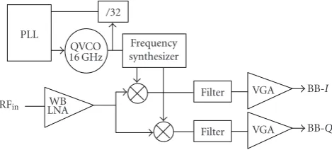
A direct conversion architecture for seven-band OFDM UWB has been proposed in [13]. The seven carrier frequen-cies are generated from a single 16 GHz VCO (seeFigure 9). The circuit has been fabricated in a 0.18µm SiGe BiCMOS process and achieves an NF of 3.3–4.1 dB and a conversion gain of 52 dB. The current consumption is 88 mA from a 2.7 V supply.
A fully integrated receiver front end has been integrated in a SiGe BiCMOS technology with an NPN-fT of 70 GHz
PLL
RFin
/32
QVCO 16 GHz
Frequency synthesizer
WB LNA
Filter
Filter
VGA
VGA
BB-I
BB-Q
Figure 9: Receiver architecture used in [13]. The PLL is imple-mented off-chip.
[21]. The block diagram and chip micrograph are shown in
Figure 10. The chip with a total area of 4 mm2has been
pack-aged in an HVQFN package and mounted on an FR4 board. Digital control blocks for tuning the VCOs and the IF filter as well as a bandgap unit have also been implemented. The measured performance is provided inTable 1[21], indicating that low noise figures can be achieved for complete receivers. The transmit chain is published in [14] and features wide-band elliptic basewide-band filters, a VGA with dynamic range of 12 dB, an up-conversion mixer, and an RF output stage with a power of−7 dBm. The current consumption is 43 mA at 2.7 V for the complete transmit path.
Finally, some interesting studies on low-power UWB transceiver architectures have been presented in [22,23]. The architectures are based on the use of distributed design ap-proaches in the LNA and down-mixer circuits.
7. CONCLUDING REMARKS
Several circuit design techniques for multiband UWB have been discussed. Challenging design aspects in UWB are the combination of wideband behavior at radio frequencies and baseband in combination with low noise figures and high lin-earity, as well as the required fast LO hopping.
RF input LNA,
mixer filterBB
BB outputs Multitone
generator
2m
m
2 mm (a)
Pre-filter LNA Mixer
Integrated on-chip
ADC
BB amplifier/filter
Synthesizer
I
Q
(b)
Figure10: Chip photograph (a) and block diagram (b) of a fully integrated UWB receiver.
Table1: Measured data of the receiver ofFigure 10(assuming 20 dB attenuation by prefilter).
Parameter Required Measured Info
Current consumption — 78 mA @ 2.5 V —
Noise figure <6.6 dB1 4.5 dB On PCB, center of IF band, LO is 3960 MHz Input IP2 >+20 dBm +25 dBm fin1: 5 GHz ISM,fin2: GSM1900 Input IP3 >−9 dBm −6 dBm fin1: 5 GHz ISM,fin2: 5 GHz ISM Maximum gain — 59 dB Power gain from RF input to base band output VCO phase noise <−100 dBc/Hz −104 dBc/Hz At 1 MHz offset
Integrated phase noise <3.5 degrees rms 1 degrees rms Integrated from 0 to 50 MHz
In-band spurs <−30 dBc <−30 dBc —
Out-of-band spurs <−50 dBc <−50 dBc For 5 GHz ISM
<−45 dBc <−45 dBc For 2.4 GHz ISM
Hopping speed <9.5 ns <1 ns For all allowed hopping sequences
1Requirement is<4.6 dB assuming a pre-filter insertion loss of 2 dB.
ACKNOWLEDGMENT
The author would like to acknowledge the much-appreciated inputs from the Philips UWB team, both in Eindhoven as well as in San Jose, Calif.
REFERENCES
[1] http://www.ieee802.org/15/pub/TG3a.html.
[2] “‘Multi-band OFDM Physical Layer Proposal for IEEE 802.15 Task Group 3a’,” IEEE P802.15 Working Group for Wireless Personal Area Networks, March 2004.
[3] B. Razavi, H.-C. Kang, C.-C. Hsu, and C.-C. Lee, “Multiband UWB transceivers,” inProceedings of the IEEE Custom Inte-grated Circuits Conference (CICC ’05), pp. 140–147, San Jose, Calif, USA, September 2005.
[4] A. Ismail and A. Abidi, “A 3 to 10 GHz LNA using a wideband LC-ladder matching network,” inProceedings of IEEE Interna-tional Solid-State Circuits Conference (ISSCC ’04), vol. 1, pp. 384–534, San Francisco, Calif, USA, February 2004.
[5] A. Bevilacqua and A. M. Niknejad, “An ultra-wideband CMOS LNA for 3.1 to 10.6 GHz wireless receivers,” inProceedings of IEEE International Solid-State Circuits Conference (ISSCC ’04), vol. 1, pp. 382–533, San Francisco, Calif, USA, February 2004. [6] P. Heydari, D. Lin, A. Shameli, and A. Yazdi, “Design of CMOS distributed circuits for multiband UWB wireless receivers [LNA and mixer],” inProceedings of IEEE Radio Frequency In-tegrated Circuits (RFIC ’05), pp. 695–698, Long Beach, Colo, USA, June 2005.
[7] P. Heydari and D. Lin, “A performance optimized CMOS dis-tributed LNA for UWB receivers,” inProceedings of the IEEE Custom Integrated Circuits Conference (CICC ’05), pp. 330– 333, San Jose, Calif, USA, September 2005.
[8] M. Tsai, K.-Y. Lin, and H. Wang, “A 5.4mW LNA using a 0.35µm SiGe BiCMOS technology for 3.1-10.6GHz UWB wireless receivers,” inProceedings of the IEEE Custom Integrated Circuits Conference (CICC ’05), pp. 337–340, San Jose, Calif, USA, September 2005.
Circuits Conference (ISSCC ’05), vol. 1, pp. 216–594, San Fran-cisco, Calif, USA, February 2005.
[10] S. Iida, K. Tanaka, H. Suzuki, et al., “A 3.1 to 5 GHz CMOS DSSS UWB transceiver for WPANs,” inProceedings of IEEE In-ternational Solid-State Circuits Conference (ISSCC ’05), vol. 1, pp. 214–594, San Francisco, Calif, USA, February 2005. [11] J. Bergervoet, K. Harish, G. van der Weide, et al., “An
interfer-ence robust receive chain for UWB radio in SiGe BiCMOS,” inProceedings of IEEE International Solid-State Circuits Con-ference (ISSCC ’05), vol. 1, pp. 200–593, San Francisco, Calif, USA, February 2005.
[12] G. Chevallier and E. F. Stikvoort, Transformer Circuit, Double-Balanced Mixer, US patent 5825231.
[13] A. Ismail and A. Abidi, “A 3.1 to 8.2 GHz direct conversion re-ceiver for MB-OFDM UWB communications,” inProceedings of IEEE International Solid-State Circuits Conference (ISSCC ’05), vol. 1, pp. 208–593, San Francisco, Calif, USA, February 2005.
[14] S. Aggarwal, D. M. W. Leenaerts, R. van de Beek, et al., “A low power implementation for the transmit path of a UWB transceiver,” inProceedings of the IEEE Custom Integrated Cir-cuits Conference (CICC ’05), pp. 148–151, San Jose, Calif, USA, September 2005.
[15] C. Grewing, K. Winterberg, S. van Waasen, et al., “Fully inte-grated distributed power amplifier in CMOS technology, op-timized for UWB transmitters,” inProceedings of IEEE Radio Frequency Integrated Circuits Symposium (RFIC ’04), pp. 87– 90, Fort Worth, Tex, USA, June 2004.
[16] D. M. W. Leenaerts, R. van de Beek, G. van der Weide, et al., “A SiGe BiCMOS 1ns fast hopping frequency synthesizer for UWB radio,” inProceedings of IEEE International Solid-State Circuits Conference (ISSCC ’05), vol. 1, pp. 202–593, San Fran-cisco, Calif, USA, February 2005.
[17] D. M. W. Leenaerts, J. van der Tang, and C. S. Vaucher,Circuit Design for RF Transceivers, Kluwer Academic, Dordrecht, The Netherlands, 2001.
[18] C.-C. Lin and C.-K. Wang, “A regenerative semi-dynamic fre-quency divider for mode-1 MB-OFDM UWB hopping carrier generation,” inProceedings of IEEE International Solid-State Circuits Conference (ISSCC ’05), vol. 1, pp. 206–207, San Fran-cisco, Calif, USA, February 2005.
[19] R. van de Beek, D. M. W. Leenaerts, and G. van der Weid, “A fast-hopping single-PLL 3-band UWB synthesizer in 0.25µm SiGe BiCMOS,” inProceedings of the 31st European Solid-State Circuits Conference (ESSCIRC ’05), pp. 173–176, Grenoble, France, September 2005.
[20] J. Lee and D. Chiu, “A 7-band 3-8 GHz frequency synthesizer with 1 ns band-switching time in 0.18µm CMOS technology,” inProceedings of IEEE International Solid-State Circuits Con-ference (ISSCC ’05), vol. 1, pp. 204–593, San Francisco, Calif, USA, February 2005.
[21] R. Roovers, D. M. W. Leenaerts, J. Bergervoet, et al., “An interference-robust receiver for ultra-wideband radio in SiGe BiCMOS technology,” IEEE Journal of Solid-State Circuits, vol. 40, no. 12, pp. 2563–2572, 2005.
[22] P. Heydari, “Design considerations for low-power ultra wide-band receivers,” inProceedings of IEEE 6th International Sym-posium on Quality of Electronic Design (ISQED ’05), pp. 668– 673, San Jose, Calif, USA, March 2005.
[23] P. Heydari, “A study of low-power ultra wideband radio transceiver architectures,” inProceedings of Wireless Commu-nications and Networking Conference (WCNC ’05), vol. 2, pp. 758–763, New Orleans, La, USA, March 2005.
D. M. W. Leenaertsreceived the Ph.D. de-gree in electrical engineering from hoven University of Technology, Eind-hoven, the Netherlands, in 1992. From 1992 to 1999, he was with Eindhoven Univer-sity of Technology as an Associate Profes-sor with the Microelectronic Circuit De-sign Group, involved in analog circuit de-sign and nonlinear circuit theory. In 1995, he was a Visiting Scholar with the
![Figure 7: Measured spectral output of the synthesizer in [16] when generating the LO for band #3.](https://thumb-us.123doks.com/thumbv2/123dok_us/916377.1110903/5.600.82.526.72.274/figure-measured-spectral-output-synthesizer-generating-lo-band.webp)