-- -- -- --
- - -
-
---
-
---- ----
-
-
--_.-GA34-0230-1
File No. 51-16
IBM Series/1
4956 Processor Models C and C 10
Description
-~---
- - -
-
-
- - - -
-
----
-
-
_.
-GA34-0230-1
File No. S1-16
IBM Series/ 1
4956 Processor Models C and C 1
a
Description
Second Edition (January 1986)
Use this publication for the purpose stated in the preface.
Changes are periodically made to the information herein; any such changes will be reported in subsequent revisions or Technical Newsletters.
It is possible that this material may contain reference to, or information about, IBM products (machines and programs), programming, or services that are not announced in your country. Such references or information must not be construed to mean that IBM intends to announce such IBM products, programming, or service in your country.
Preface
This publication describes the unique functional characteristics of the IBM Series/ I 4956 Processor Models C and CIO, and the processor optional features. Refer to the IBM Series/1 Principles of Operation, GA34-0152, for the common Series/I processor functional characteristics and instructions. This publication also provides reference information about the following:
Processor and processor feature configurations
Processor and processor feature operations.
The reader should understand data processing terminology and be familiar with binary and hexadecimal numbering systems.
The publication is intended primarily as a reference manual for experienced programmers who require machine code information to plan, correct, and modify programs written in the assembler language.
Chapter 1. Introduction contains a general description of the processor, processor storage, and processor features.
Chapter 2. Main Storage Addressing Using the Relocation Translator describes the relocation translator, including: '
Relocation addressing
Storage protection mechanism
• Error-recovery considerations
Chapter 3. Console describes the keys, switches, and indicators for the basic console and the optional programmer console. Typical manual operations, such as storing into and displaying main storage, are presented.
Chapter 4. Diagnose (DIAG) Instruction describes the Diagnose instruction.
Chapter 5. Diskette Data Format describes how data and control information are formatted on the diskette surfaces.
Chapter 6. Input/Output Operations describes the I/O commands and control words that are used to operate the diskette unit. Condition codes and status information relative to the I/O operation are also explained.
Appendix A. Instruction Execution Time contains information for determining instruction execution time and instruction throughput.
Appendix B. Software Notes lists some software notes for the processor and the diskette drive unit.
Appendix C. Error Log describes the error log and explains its use as an aid in isolating errors.
Prerequisite Publication
Contents
Chapter 1. Introduction 1-1 Card Plugging Assignments 1-3 Processor Description 1-4
Input/Output Units, I/O Features, and Processor Options 1-7 Diskette 1-8
Diskette Protection 1-10
Chapter 2. Main Storage Addressing Using the Relocation Translator 2-1 Translator Description 2-1
Storage Mapping 2-2 Relocation Addressing 2-2
I/O Storage Access Using the Relocation Translator 2-4 Status of Translator After Power Transitions and Resets 2-4 Error-Recovery Considerations 2-5
Invalid Storage Address (ISA) 2-5 Protect Check 2-5
Address Space Management 2-6 Active Address Key 2-6
Equate Operand Spaces (EOS) 2-6 Address Space 2-7
Address Key Values After Interrupts 2-9
Chapter 3. Console 3-1 Basic Console 3-2
Indicators 3-3 Programmer Console 3-3
Console Display 3-4 Indicators 3-5
Combination Keys/Indicators 3-6 Keys and Switches 3-12
Displaying Registers 3-17 Storing Into Registers 3-17
Displaying Segmentation Registers 3-18 Storing Into a Segmentation Register 3-19 Displaying Main Storage Locations 3-21 Storing Into Main Storage 3-23
Chapter 4. Diagnose (DIAG) Instruction 4-1 Storage Select 4-3
Storage Select Word 4-3
Storage Select Byte/ECC Code Bits 4-4 Local Storage Register Select 4-5
Channel Select 4-6 Set System ID 4-6 Error Log Select 4-7 Indicators 4-7
Program-Check Condition 4-7
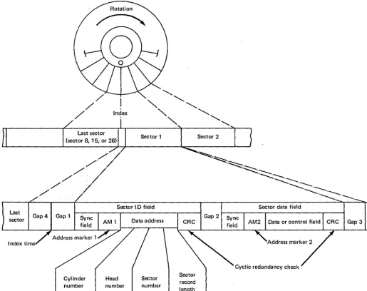
Chapter 5. Diskette Data Format 5-1 Track Format 5-2
Diskette Labels 5-8
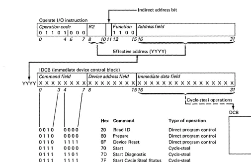
Chapter 6. Diskette Drive Input/Output Operations 6-1 Direct Program Control (DPC) 6-3
Prepare 6-4 Read ID 6-4" Device Reset 6-5 Halt I/O 6-5 Cycle-Steal 6-6
Start 6-8 Seek 6-18
Recalibrate Head 6-19 Format Track 6-20
Format Track Defective 6-22 Set FM/MFM Bit 6-23
Verify Format Track/Compare Data 6-24 Read Data 6-25
Read Verify/Cyclic Redundancy Check 6-28 Read Verify/Compare Data 6-30
Read Sector ID 6-32 Read Diagnostic Record 6-35 Write Data/Data Address Marker 6-38 Write Data/Control Address Marker 6-40 Write Data With Read Verify 6-42 Read Attachment Storage 6-44 Write Attachment Storage 6-44 Start Cycle Steal Status 6-45 Start Cycle Steal Diagnostic 6-52 Automatic Seek Option 6-53 Spiral Operation 6-54 Condition Codes 6-56
Operate I/O Instruction 6-56 Interrupt 6-57
Status Information 6-58
Interrupt Identification Word 6-58 Interrupt Status Byte 6-59 Error-Recovery Procedures 6-60 Resets 6-63
Initial Program Load OPL) 6-64
Appendix A. Instruction Execution Times A-I
Appendix B. Software Notes B-1 Notes for Processor B-1 Notes for Diskette Drive B-2
Appendix C. Error Log C-J
Purpose C-I Structure C-I
Machine Check C-2 Program Check C-2
Stall Detector/Timer Overrun Error C-2 Format of Log Entries C-3
Machine Check C-3 Program Check C-3 Priority Interrupt Entries C-4 Operate I/O Entries C-4
Chapter 1. Introduction
The IBM Series/l 4956 Processor Models C and CI0 are compact general-purpose computers. The models are the same, except for base storage. Model C has 256 or 512 kilobytes of base storage; modet'Cl0 has 1024 kilobytes of base storage.
The processor is microcode-controlled for both automatic functions and program instruction functions. It includes one self -contained diskette drive as standard, and a second self -contained diskette drive may be added as an option.
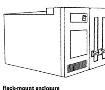
The processor is a full-rack unit that can be mounted in a standard 483-millimeter (19-inch) rack. An optional stand-alone enclosure feature is also available, making this computer suitable for placement outside a rack (see Figure 1-1).
The processor contains four card sockets for data channel features and a channel rep ower card. One of the four card sockets must be used for the internal diskette drive attachment card, and two card sockets may be used for cards with additional processor storage.
Rack-mount enclosure (front view)
[image:8.634.178.350.294.441.2]Stand-alone enclosure (front view)
Figure 1-1. IBM Series/l 4956 Processor Models C and CI0
The processor has the following characteristics:
Four priority interrupt levels, with independent registers and status indicators for each level.
Automatic and program-controlled level switching.
An instruction set that includes stacking and linking facilities, multiply and divide, variable-field-length byte operations, and a variety of arithmetic and branching instructions.
Supervisor and problem states.
A basic console that is a standard feature; a programmer console that is an optional feature.
A storage address relocation translator that allows addressing of main storage larger than 64 kilobytes.
An error correction code (ECC) that is implemented on the storage card to provide the capability for single-bit error correction and double-bit error detection.
An error log, which provides a history of errors that have occurred since power-on.
A clock/comparator. Four instructions are provided to set or copy the clock and comparator.
Channel capability:
Asynchronous, multidropped channel
256 input/output (I/O) devices can be addressed
Direct program control and cycle-steal operations
Maximum burst output data rate of 1.11 million 16-bit words per second (see Note)
Maximum burst input data rate of 1.54 million 16-bit words per second (see Note)
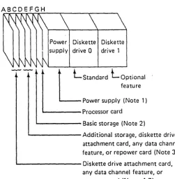
Card Plugging Assignments
The processor unit contains power and space for additional features. The IBM 4959 Input/Output Expansion Unit and the IBM 4965 Diskette Drive and I/O Expansion Unit are available for adding additional features, if desired.
Figure 1-2 shows the card plugging assignments for the processor.
Diskette Diskette drive 0 drive 1
!
1
LStandard LOptionalfeature
Power supply (Note 1) Processor card
~---Basic storage (Note 2)
io---Additional storage, diskette drive attachment card, any data channel feature, or repower card (Note 3) ' - - - Diskette drive attachment card,
any data channel feature, or repower card (Notes 4-7)
Figure 1-2. Card Plugging Assignments
Notes:
1. The pluggable high-frequency power supply plugs into card socket H. 2. The processor contains 256 KB (kilobytes), 512 KB, or 1024 KB of basic
storage in socket E.
3. The processor supports three different size storage cards: 256 KB, 512 KB, and 1024 KB. Sockets C and D are available for additional storage. Any
combination of storage cards may be used to obtain the desired system storage size, up to the maximum of 1024 KB. Sockets not used for additional storage can be used for the diskette drive attachment card, any channel feature, or a repower card.
4. A single diskette drive attachment card is used with either one or two diskette drives.
5. The diskette drive attachment card can be plugged into any I/O card socket position to establish the desired priority.
6. If a repower card is used, it must be plugged to the left of and adjacent to the leftmost I/O card installed.
7. A maximum of five serially connected channel repower features can be driven by each processor. Any processor system thflt includes an IBM I/O expansion unit with the two-channel switch feature is limited to three channel repower features.
[image:10.624.219.471.163.419.2]Processor Description
I
I
I
I
I
I
I
I
L
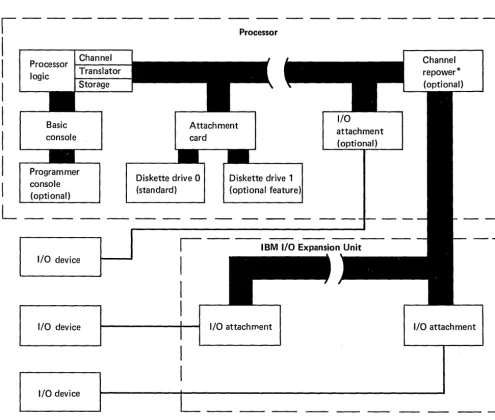
Processor logic Basic console Programmer console (optional)I/O device
I/O device
I/O device
The basic processor includes the processor card, a 256K-byte, 512K-byte, or 1024K-byte storage card, a basic console, one diskette drive (drive 0), and a diskette drive attachment card. Figure 1-3 shows a block diagram of the processor and an IBM 4959 I/O Expansion Unit.
Processor
- I
Attachment card
Diskette drive 0 (standard)
Diskette drive 1 (optional feature)
attachment (optional)
r
-I IBM I/O Expansion UnitI/O attachment
Channel
I
I
I
I
I
I
I
I
~
-l
I/O attachment
I
I
I
I
I
I
[image:11.624.49.544.142.561.2]* Required with an expansion unit.
Four priority interrupt levels (0-3) are implemented in the processor. Each level has an independent set of machine registers. Level switching can occur in two ways: (1) by program control, or (2) automatically upon acceptance of an I/O interrupt request. The interrupt mechanism provides 256 unique entry points for I/O devices.
Note: A Prepare command to levels 4-15 is executed so that condition code reporting occurs; however, the Prepare command is not executed at the addressed device and effectively results in a no-operation.
The processor instruction set contains a variety of instruction types. These include: shift, register to register, register immediate, register to (or from) storage, bit manipulation, multiple register to storage, variable byte field, and storage to storage. Supervisor and problem states are implemented, with appropriate privileged instructions for the supervisor.
The basic console is intended for dedicated systems that are used in a primarily unattended environment. Only minimal controls are provided. A programmer console, which can be added as a feature, provides a variety of indicators and controls for operator-oriented systems.
The processor supports three different size storage cards: 256 KB, 512 KB, and 1024 KB. The processor has a maximum of 1024 KB of storage. Up to two additional storage positions are available. Any combination of storage cards may be used to obtain the desired system storage size, up to the maximum of 1024 KB. (The relocation translator must be enabled to select addresses above 64K bytes.)
An error correction code (ECC) is implemented on the storage card. ECC gives the storage card the capability of single-bit error correction and double-bit error detection. ECe provides the user a higher system availability.
Note: When a double-bit error in storage is detected during a processor read, a machine check interrupt occurs with PSW bit 8 set to 1 (storage parity error).
There is no storage-protect feature in the 4956 processor. However, there is a read-only protect capability provided by the address translator when it is enabled.
Note: Execution of the Set Storage Key (SESK) and Copy Storage Key (CPSK) instructions results in a no-operation.
I/O devices are attached to the processor through the processor data channel. The data channel directs the flow of information between the I/O devices, the
. processor, and main storage. The data channel supports a maximum of 256 addressable devices.
The data channel supports:
Direct program control operations. Each Operate 110 instruction transfers a byte or word of data between main storage and,the device. The operation may or may not terminate in an interrupt.
• Cycle-steal operations. Each Operate 110 instruction initiates mUltiple data transfers between main storage and the device. The maximum cycle-steal transfer per device control block (DCB) is 65,535 bytes. Cycle-steal operations are overlapped with processor operations and always terminate in an interrupt.
Input/Output Units, I/O Features, and Processor Options
The floating-point feature is one of the available options. If the floating-point feature is installed, refer to Appendix A for instruction execution times. For a detailed description of this feature, refer to the IBM Series/l Principles of
Operation, GA34-0152.
A variety of I/O units and features, plus several processor options, are available for use with the Series/l processor. For a list and description of system units and features, refer to the IBM Series/l System Selection Guide, GA34-0143, and the
IBM Series/l Digest, G360-0061. Detailed information about I/O units and features can be found in separate publications. The order numbers for these publications are contained in the IBM Series/l Graphic Bibliography, GA34-0055.
Diskette,
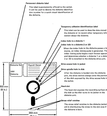
The diskette storage medium is a flexible magnetic disk that is permanently enclosed in a jacket. The disk and jacket together are referred to as a diskette (see Figure 1-4). Small slots in the jacket allow the read/write heads to contact the surfaces as the disk rotates within the jacket (see Figure '1-5). '
Three types of diskettes are used in the diskette drive:
Diskette 1. This diskette is intended for the recording of single-density (FM) data on one diskette surface (side 0).
Diskette 2. This diskette is intended for the recording of single-density (FM) data on both diskette surfaces (sides 0 and
O.
Diskette 2D. This diskette is intended for the recording of double-density (MFM) data on both diskette surfaces (sides 0 and
O.
Note: Index holes on the one-sided and two-sided diskettes occupy different locations on the diskette.
Diske~~
One-sided diskette (diskette 1)
Index hole
[image:15.626.118.552.314.660.2]--203mm (8 in.)
Diskette No.
IBM Diskette
Permanent diskette label
This label is permanently affixed to the jacket. I t can be used to denote the diskette identifica-tion number for a quick visual identificaidentifica-tion of the diskette.
Payroll Detail
Temporary adhesive identification label
This label can be used to describe data stored on the diskette or to record other temporary infor-mation about the diskette.
Index hole in a diskette 1
Index hole in a diskette 2 or 20
When the index hole in the diskette passes a light source, an index timing pulse is generated. The index timing pulse begins track format operations and determines whether a diskette 1 or a diskette 2 or 20 is installed in the diskette drive unit.
Drive access hole in jacket
Drive spindle hole in disk
After the diskette is loaded into the diskette unit, the drive station clamps onto the portion of the disk exposed by the drive access hole in the jacket.
The head slot exposes the recording surface of the disk as the disk turns in its jacket in the diskette unit.
Stress relief notches
The stress relief notches in the diskette jacket aid in distributing the stress in the slot area if the diskette is bent.
Figure 1-5. Diskette Characteristics
[image:16.626.166.579.68.514.2]Diskette Protection
To prevent damage to diskettes or the loss of data that has been recorded on them, diskettes should be handled with care at all times. The following precautions should be observed:
Return diskettes to their envelopes whenever they are removed from the diskette drive.
IBH
Disk.
YES
Do not lay diskettes near food, drink, or ashtrays.
Do not use clips or rubber bands on diskettes.
NO
Do not place heavy objects on diskettes.
Do not touch or attempt to clean diskette surfaces. Contaminated diskettes must be discarded.
NO
Do not place diskettes near materials that might be magnetized. (Data can be lost from a diskette that is exposed to a magnetic field.)
NO
• Do not expose diskettes to heat greater than 51.50
C (1250
F) or to direct sunlight.
Storage
Shipping
When diskettes are not in use, they should be placed in their protective envelopes and stored in the following environment:
Relative humidity: 8 % to 800/0
• Maximum wet bulb: 29.4°C (85°F)
If a diskette has been exposed to an environment outside of the given range, the diskette should be given at least five minutes to acclimate to a suitable environment before use. During that time, the diskette should be removed from its shipping container.
Diskettes should be shipped only in special shipping cartons (available from IBM). With the diskette in..place, the package weighs 280 grams (10 ounces).
Shipping cartons should be labeled:
DO NOT EXPOSE TO HEAT OR SUNLIGHT
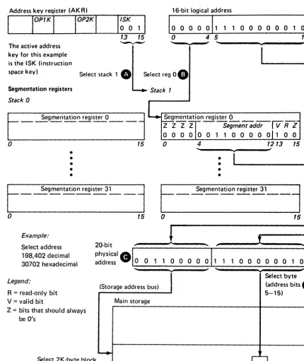
Chapter 2. Main Storage Addressing Using the Relocation Translator
Translator Description
Segmentation registers Stack 0 Segmentation rego
Segmentation reg 1•
•
•
•
•
•
Segmentation reg 31o
15The relocation translator and segmentation registers permit addressing of main storage locations beyond 64K bytes and provide a read-only type of storage protection. The first 64K bytes can be addressed directly when the translator is disabled; therefore, the translator must be enabled when main storage above 64K bytes is accessed.
The translator provides eight stacks of 16-bit segmentation registers. The stacks are numbered 0- 7 to correspond to the eight possible values of the address keys. Each stack consists of 32 registers (0-31):
Stack 1 Segmentation reg
o
Segmentation reg 1•
•
•
•
•
..
Segmentation reg 31o
• • •
• •
• •
•
• •
•
• •
•
•
• •
•
•
•
15 Stack 7 Segmentation rego
Segmentation reg 1•
•
•
•
•
•
Segmentation reg 31o
15The stacks of segmentation registers are under supervisory program control. Four privileged instructions are used with the relocation translator and segmentation registers.
Set Segmentation Register (SESR). This instruction loads one segmentation register.
Copy Segmentation Register (CPSR). This instruction allows the supervisor to inspect the contents of a segmentation register.
Enable (EN). This instruction enables the relocation translator. Until the translator is enabled, 16-bit addressing is in effect for the low-order 64K bytes of storage. Any storage above 64K bytes is not accessible to the program until the translator is enabled.
Disable (DIS). This instruction disables the relocation translator.
Refer to the IBM Series/1 Principles of Operation, GA34-0152, for detailed descriptions of the preceding instructions.
Storage Mapping
Relocation Addressing
Mapping of main storage is achieved through the segtp.entation registers. Each segmentation register controls a 2K-byte segment of storage. The SESR instruction is used to load each segmentation register with the unique physical address of a 2K-byte segment of storage.
Note: More than one segmentation register can be loaded with the same segment address. For example, stack 0, register 15 (associated with the supervisor address key of 0), can be loaded with the same number as stack 1, register 6. This arrangement allows the supervisor to address control blocks within a problem program even though the address key for the supervisor is different than the key for the problem program. Once loaded, each stack of segmentation registers contains a complete map of 64K bytes divided into 2K-byte physical segments.
The relocation translator generates a physical address that allows any byte in storage to be addressed. Figure 2-1 shows an example of address translation. The letters in the following description correspond to the letters in Figure 2-1:
" The active address key from the address key register selects a segmentation register stack. The address key pertains to the instruction being executed on the current priority level.
o
The five high-order bits (0-4) of the 16-bit address (generated for theinstruction being executed) select a segmentation register within the stack selected in description
O.
These bits define the logical segment.e
The physical address is generated. The high-order bits are from thesegmentation register; these bits specify the physical address of a 2K-byte segment of storage.
Bit 13 - Valid Bit: When set to 1, this bit specifies that the contents of the segmentation register are valid; the segmentation register can be used to perform the translation. When bit 13 is a 0, the segmentation register cannot be used for translation (no access). If translation is attempted, a program-check interrupt occurs with invalid storage address set in the processor status word (PSW). (All valid bits are set to O's after power is switched on.)
Bit 14 - Read-Only Bit: When set to 1, this bit specifies that the block is read-only.
If an attempt is made to write into storage using a segmentation register with the read-only bit set to 1, a program-check interrupt occurs with protect check set in the PSW. Storage is not changed. Bit 14 is ignored by a cycle-steal access or when the processor is in supervisor state.
Address key register (AK R) 16-bit logical address
1000 0 01, , , 0 0 0 0 0 0 , 01 13 15
~
o
4 5 15
The active address key for this example is the 15K (instruction
'----~---' ~,---~---~,
space key) Select stack 1
e
Select reg 0G
Segmentation registersStack 0
Segmentation register 0
f
-o
•
•
•
•
•
Segmentation register 31
15
~-
-- --
- -- --
---o
15Example:
Stack 1
Seg~tation regi~
2- _-_ __
__
Z Z Z Z Segment addr
Iv
R Zo
0 0 0 0 0 1 1 0 0 0 0 0 1 0 0o
1213 15o
•
•
•
•
Segmentation register 31
,
15
2 0 - b i t , . ~
Select address 198,402 deci mal 30702 hexadecimal
physical
AI
I
I
address V _ 0 0 1 1 0 0 0 0 0 1 1 1 0 0 0 0 0 0 1 0
Legend:
(Storage address bus)
R = read-only bit
V
=
valid bitZ = bits that should always be O's
Select 2K-byte block
Note: When the translator is
[image:24.634.148.579.69.581.2]-+-disabled, address bits 0-15 only are used for main storage address selection.
Figure 2-1. Address Translation Example
Main storage
,. .... -,
I
Select byte(address bits
•
5-15),
C'=l
I/O Storage Access Using the Relocation Translator
All storage access requests from I/O devices are translated by the same hardware that handles storage requests from the processor. The device control blocks (DCBs) must reside in the supervisor's address space; therefore, all I/O devices must use address key 0 to gain access to the DCBs and to store the individual residual status blocks. The address key of the process 'requiring a cycle-steal operation resides in a DCB. An I/O device presents this address key, along with a 16-bit logical address, to the relocation translator. This allows an I/O device to directly address the storage space for a particular process. The address key allows I/O storage protection to be established between address spaces, assuming that the supervisor ensures the integrity of the DCBs.
Status of Translator After Power Transitions and Resets
The translator is enabled by the Enable (EN) instruction, or by the PSW key of the programmer console, if installed. The translator is disabled by any of the
following:
Disable (DIS) instruction
• Power-on reset
Check Restart key on programmer console
Initial program load (IPL)
System Reset key on programmer console
All translator controls are reset when the translator is disabled.
Notes:
1. A machine-check interrupt does not disable the translator.
2. The segmentation registers are not reset when the translator is disabled.
Error-Recovery Considerations
Invalid Storage Address (ISA)
Protect Check
The invalid storage address bit (bit 1 of the PSW) is set to 1 by anyone of the following:
Storage access was attempted using a physical address greate~ than the physical storage size installed.
Storage access was attempted with bit 13 (valid bit) of the segmentation register set to 0. This signifies that the contents of the segmentation register are invalid.
The specific nature of the invalid storage address can be resolved as follows:
Store the segmentation register following the program-check interrupt.
Test the value of bit 13 in the selected segmentation register. When set to 1, this bit specifies that the contents of the segmentation register are valid; the segmentation register can be used to perform the translation. When bit 13 is a 0, the segmentation register cannot be used for translation (no access). If
translation is attempted, a program-check interrupt occurs with invalid storage address set in the processor status word (PSW).
Ensure that the segment address does not exceed the limits of the physical processor storage installed.
When the translator is enabled, a program-check interrupt with protect check set in the PSW is caused by an attempt to write into storage, while in the problem state, using a segmentation register with bit 14 (read-only) set to 1.
Storage is not changed. Bit 14 is ignored by a cycle-steal access, or when in supervisor state.
Address Space Management
Active Address
Key
Cycle-steal devices have a cycle-steal address key specified in their device control block.
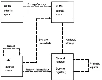
Anyone of the four address keys (ISK, OPIK, OP2K, or the cycle-steal address key) may be used during a storage access as the active address key. The address key in use (active) depends on the type of operation being performed at a specific instant in time. The active address key defines storage access through a particular block of segmentation registers.
Each priority level in the processor has an associated address key register (AKR) that contains three address keys and an equate-operand-spaces (EOS) bit.
Address key register (AKR)
o
1t
EOS EOS
4 5 789 111213 15
~ ~ ---...-'
OP1K OP2K ISK
Equate operand spaces. This bit, when set to 1, causes all data operands to use the OP2K address key. See "Equate Operand Spaces (EOS)" in this chapter.
OP1 K Operand 1 key. These bits contain the binary-coded operand 1 address key, with bit 7 as the low-order bit.
OP2K Operand 2 key. These bits contain the binary-coded operand 2 address key, with bit 11 as the low-order bit.
ISK Instruction space key. These bits contain the binary-coded instruction-space address key, with bit 15 as the low-order bit.
Equate Operand Spaces (EOS)
The equate operand spaces bit (bit 0) in the address key register controls the use of the OPIK address key.
When the EOS bit is set to 1 (enabled), all processor data fetches use a single address space defined by the OP2K address key. The OPIK is ignored, but not changed, and all normal OPIK operations use OP2K as an active key. When the EOS bit is set to 0 (disabled), the OPIK address key functions in a normal manner.
Address Space
When the relocation translator is enabled, an address key defines a specific address space where:
The address space is a range of logically contiguous storage.
The address space is accessible by the effective address without operating system intervention (the address space is not greater than 64K bytes).
All instruction fetches use the address space defined by the instruction space key (lSK). For storage-to-storage instructions, all reads and writes for data operand 1 use the address space defined by the OP 1 K, assuming that the EOS bit is a O. All other storage data accesses, reads, and writes use the address space defined by the OP2K, excluding branch and jump instructions.
Examples:
ISK=OPIK=OP2K. For instruction processing, all storage accesses occur within the same address space.
ISK,=OPIK,OPIK=OP2K. Instruction fetches occur in the ISK address space_. Data access occurs in the OP2K address space.
ISK,=OPIK,OPIK,=OP2K. Refer to Figure 2-2 for this example.
I/O operations that access main storage also use an address key. Cycle-steal operations (read or write) use the cycle-steal address key specified within the device control block. An address key of 0 is used when the device fetches the device control block. Direct program control (OPC) operations that write data to storage use the OP2K address key.
Other defined uses of the address key register are as follows:
All indirect access for branching uses the ISK.
Effective-address generation occurs in the address space of the particular data operand. The appended words in the instruction are accessed by the ISK.
Storage access from the console is defined by the SAR address key.
Stop-on-address is based on the Stop On Address key when the translator is enabled.
System reset and IPL set all address keys and the EOS bit to O's.
OP1K ~---. Storage/storage OP2K
address address
space space
r-I
I
I
I
Register/I
Storage immediate storageBranch
I
~--.,
I
I
I
General
ISK _ _ .J
I
---,
registers
I
Re~ister/ addressspace
- - - - -
Register immediate (system registers)Assembler syntax for address spaces (see Appendix A)
ISK
Bits 13-15 ofAKR Bits 13-15 ofAKR OP1K addr5 (reg) *Indirect addressing. Notes: OP2K addr4 (reg) Example instructions AW MVFD MVBI B addr5,addr4 (reg), (reg) byte,reg longaddr*
_.J
register1. OP1 K is only used for the source operand in storage-to-storage operations. 2. OP2K is used for storage data access in all other operations (excluding
branch/jump).
[image:29.612.179.522.62.334.2]3. ISK (bits 13-15 of the AKR) is used for instruction fetch and branch/jump operations.
Address Key Values After Interrupts
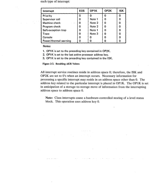
When priority or class interrupts occur, certain values are set in the address keys of the affected AKR. These values anticipate the address spaces that the programmer might need for interrupt processing. Figure 2-3 shows the resulting AKR values for each type of interrupt:
Interrupt EOS OP1K OP2K ISK
Priority 0 0 0 0
Supervisor call 0 Note 1 0 0
Machine check _ ..
0 Note 2· 0 0
Program check 0 Note 2 0 0
Soft-exception trap 0 Note 1 0 0
Trace 0 Note 3 0 0
Console 0 0 0 0
Power/thermal warning 0 0 0 0
Notes:
[image:30.627.80.578.117.732.2]1. OP1 K is set to the preceding key contained in OP2K. 2. OP1 K is set to the last active processor address key. 3. OP1 K is set to the preceding key contained in the 15K.
Figure 2-3. Resulting AKR Values
All interrupt service routines reside in address space 0; therefore, the ISK and OP2K are set to O's when an interrupt occurs. Necessary information for processing a specific interrupt may reside in an address space other than O. The address key related to the particular interrupt is placed in OPIK. The OPIK is set in anticipation of a storage-to-storage move of information from the interrupting address space to address space O.
Note: Class interrupts cause a hardware-controlled storing ofa level status block. This operation uses address key O.
Chapter 3. Console
The basic console is standard; the programmer console is an optional feature.
IPL Source
~~[d
Pro mary~
Alternate
(;;-'°°1
Mode
CJ
OW."
Auto IPL~
Normal
Oft D,agnost'c
uuLJLJOOOD
LJLJLJ ::..
DODO
LJ
LJLJLJ
DODD
[J[J[Jl]ODDD
Basic console
Programmer console
The basic console is intended primarily for those systems that are totally dedicated to a particular application, where operator intervention is not needed during the execution of the application.
The programmer console is intended for operator-oriented systems where various programs are entered and executed. This type of environment requires a more versatile console arrangement for program and machine problem determination, and for manual alteration of data and programs in storage.
Basic Console
Each 4956 comes equipped with a basic console, which provides the following:
Power On/Off switch for the processor unit
IPL Source switch to select a primary or alternate IPL device
Load key for initial program load (lPL)
Mode switch to select: Auto IPL, Normal, or Diagnostic mode
Load, Wait, Run, and Power On indicators
'0
Power On/Off: When this switch is set to the On position, power is applied to the processor unit. After all power levels are up, the Power On indicator is turned on. When this switch is set to the Off position, power is removed from the processor unit and the Power On indicator is turned off.e
IPL Source: This switch selects the I/O device to be used for program loading. In the Primary position, the device that was pre-wired as the primary IPL device is selected. In the Alternate position, the device that was pre-wired as the alternate IPL device is selected.o
Load: Pressing this key causes a system reset, and the initial program load (lPL) sequence is started. The Load indicator is turned on and remains on until the IPL sequence is completed. When the IPL sequence is completed, instruction execution begins at location 0 on priority level O.e
Mode: This switch has the following positions:Auto IPL-In this position, an IPL is initiated after a successful power-on sequence. Bit 13 of the PSW is set to indicate to the software that an automatic.IPL was performed. In this mode, Stop instructions are treated as no-ops.
Normal-In this position, Stop instructions are treated as no-ops.
Diagnostic-This position has no function without the programmer console. This position places the processor in diagnostic mode if the programmer console is attached. When the processor is in diagnostic mode, Stop instructions cause the processor to enter the stop state.
o e e
IPL SourceG
(~
][;. ][; ) :.:::.
~
CD (;-
0"]
0
O
Load Auto IPLMo~dee
CJ"
O
NormalOff
Indicators
Programmer Console
o
Load: On when the machine is performing an initial program load (IPL).o
Wait: On when an instruction that exits the active level has been executed and no other priority interrupts or levels are pending.G
Run: On when the machine is executing instructions.G
Power On: On when the proper power levels are available to the system.The programmer console is an optional feature that can be ordered with the 4956 or field-installed at a later date. The programmer console provides the following:
Start and stop of the processor.
Ability to display or alter any storage location.
System reset.
Selection of anyone of the four interrupt levels for the purpose of displaying or altering data.
Displaying or altering of the storage address register (SAR), instruction address register (IAR), SAR address key register (AKR), stop-on-address address key register (AKR), level address key register (AKR), segmentation registers, console data buffer, or any general purpose register.
Displaying, but not altering, the level status register (LSR), current instruction address register (CIAR), op register, or processor status word (PSW). Note that the following bits of the PSW and LSR may be altered: PSW bit 14 (translator enabled), LSR bit 8 (supervisor state), and LSR bit 11 (summary mask).
Stop on address.
Stop on error.
Instruction stepping.
Check restart.
Request for a console interrupt.
Check indicator. The Check indicator is a light emitting diode (LED) that lights when a machine check or program check class interrupt occurs.
Lock console.
CE mode. The CE mode is used to display the error log.
The programmer console is touch-sensitive, with an audio-tone generator providing an audio response tone whenever a key is pressed and the information has been accepted and serviced by the processor.
Console Display
Run or Wait State
Stop State
When the processor is in run or wait state, the console data buffer is displayed in the data display indicators. An exception to this is when a Set Console Data Lights (SECON) instruction writes a message to the data lights and does not change the buffer. When the Data Buffer key is pressed, the console data buffer is again displayed.in the indicators.
When the console data buffer is being displayed, the console data buffer and the' display are changed by entering new data with the data entry keys.
When the processor enters stop state, the JAR is displayed in the data display indicators. Any system resource that has a corresponding select key on the console can be displayed. For example, the console data buffer can be displayed by pressing the Data Buffer key.
}
~ ~Console data buffer
IAR displ ayed in
LJLJLJDOODD
LJLJLJ
~~,.
DODD
stop stat e
LJLJLJLJOODD
LJLJLJLJODOD
Power-On Reset
Displayable areas or
message from Set Con Data Lights instructio
sole
n
Indicators
o
Data Display: When the processor is in run state, the console data buffer is displayed in the data display indicators.The Set Console Data Lights (SECON) instruction can write a message to the data display.
When the processor enters stop state, the IAR is displayed until another system resource is selected.
To display the contents of the console data buffer after a system resource has been displayed, press the Data Buffer key
e
o
Check: On when a machine-check or program-check has been recognized. The Check indicator is turned off by:Clearing the check condition.
Reset key.
Load key.
Executing a Copy Processor Status and Reset (CPPSR) instruction. This instruction resets bits 0-12 of the PSW.
Pressing any console key while in the stop state. The check condition is not cleared unless the Reset key or the Load key is pressed.
While in the stop state, the Check indicator is used to indicate main storage parity errors or invalid storage addresses during display operations. Refer to "Displaying Main Storage Locations" in this chapter.
LJLJLJLJOODD
LJLJLJ
~:.".
DODO
LJOLJDOODD
LJLJLJLJODDD
Combination Keys/Indicators
There are six combination keys/indicators:
Lock
• Stop
Stop On Address
• Instruct Step
Check Restart
Stop On Error
LJLJLJDODDD
fRlrmlfRl
MainDODD
LJLJLJ
StorageLJO[][]OODD
DLJLJLJODOD
o
Lock: Pressing the Lock key first (Lock LED begins flashing), then pressing four hex keys and the Store key locks the console. A locked console is indicated by an illuminated indicator on the Lock key. The data LEOs are automatically set to the previous value. Displays or alterations cannot be performed with theprogrammer console keys while in the Lock mode. The console remains locked until the same sequence of hex keys that locked the console is repeated and then followed by pressing the Store key.
The only data displayed during the lock mode is data set by the program or data displayed during a maintenance procedure (CE) mode.
CE Mode: The CE mode may be used (to allow the user to display the error log) by the following:
1. Press the Lock key; the Lock LED flashes.
2. Press the hex keys in the sequence: C, E, 0, O.
3. Press the Store key; the most recent entry in the error log is indicated by the display LEDs.
4. Press the Lock key once; the previous entry in the error log is indicated by the display LEDs. The Lock key may now be pressed as many times as desired. Each time the Lock key is pressed, the next previous error log entry appears on the display LEDs. (Refer to Appendix C for a description of the error log.)
Other keys may be pressed between subsequent operations of the Lock key. CE mode is exited when all 64 entries have been displayed, or when the Store key is pressed immediately after the Lock key is pressed.
Upon entering a lock/unlock/CE mode sequence, the Lock LED flashes. The SECON instruction is disabled until the lock/unlock/CE mode sequence is terminated. The console data LEDs then assume their former value, their value upon entering stop state if in stop state, or the last value sent to them if SECON instructions have occurred.
o
Stop: This indicator is on when the processor is in the stop state. Stop state is entered in the following ways:By pressing the Stop key.
In run state, the current instruction is completed.
In wait state, stop state is entered directly.
In stop state, the contents of the instruction address register OAR) prior to entering the present stop state are restored to the IAR and displayed in the data display indicators. The level that was active upon entering stop state is reselected (becomes active).
By execution of the Stop instruction (diagnostic mode only).
When an address compare occurs in stop-on-address mode.
When an error occurs in stop-on-error mode.
By pressing the Reset key.
When a power-on reset occurs.
By selecting instruction-step mode while in run state.
The Stop On Address key and the Instruct Step key are mutually exclusive. When one is pressed, the other is reset if it is on.
e
Stop On Address: Pressing this key places the processor in stop-on-address (SOA) mode and turns on the Stop On Address indicator. Pressing this key a second time resets stop-on-address mode and turns off the indicator.e
Instruct Step: Pressing this key places the processor in instruction-step mode and turns on the Instruct Step indicator. Pressing this key a second time resets instruction step mode and turns off the indicator.If the processor is in run or wait state, pressing this key causes the processor to enter stop state. Pressing the Instruct Step key a second time resets
instruction-step mode; the processor remains in stop state.
To operate in instruction step mode:
1. Key the desired starting address and store into the IAR.
2. Press the Instruct Step key.
3. Press the Start key. The instruction located at the selected address is executed, and the processor returns to stop state. The IAR is updated to the next instruction address; this address is displayed in the data display indicators.
Each time the Start key is pressed, one instruction is executed and the IAR is updated to the next instruction address.
Stop-On-Address Mode
The processor must be in stop state to set the compare address.
Stop On Address (Relocation Translator Disabled)
I. Press the Stop On Address key.
Contents of the stop-on-address register are indicated by the display LEDs.
2. Enter the selected stop-an-address address by pressing the hex entry keys for a four-digit hex address.
3. Press the Store key.
Contents of the updated stop-an-address register are indicated by the display LEDs.
4. Press the Start key.
Execution begins at the current IAR address on the level that was active prior to entering the stop state.
When the selected address is loaded into the SAR, the processor enters the stop state. If a stop-on-address compare occurs during the instruction fetch, the stop state is entered immediately with the compare SAR address indicated by the display LEDs. If a stop-on-address compare occurs during an operand fetch/store, the stop state is entered after completing the instruction and the next instruction address is indicated by the display LEDs. To exit stop state, press the Start key; execution begins at the next sequential address.
If the selected address is an instruction address:
When the compare occurs, the stop state is entered with the compare SAR address displayed in the data display indicators.
Certain machine conditions occur that cause the stop state to be entered on the wrong instruction address. When this happens, continue to press the Start key until the selected instruction address is displayed.
Stop On Address (Relocation Translator Enabled)
1. Press the Stop On Address key.
Contents of the stop-an-address (SOA) register are indicated by the display LEDs.
2. Press the AKR (address key register) key.
Contents of the stop-an-address address key register are displayed.
3. Enter the desired address key by pressing one hex entry key for a digit value (hex 0 through 7).
4. Press the Store key.
Contents of the updated stop-an-address key register are displayed.
5. Press the Stop On Address key.
Contents of the stop-an-address register are indicated by the display LEDs.
6. Enter the selected compare address by pressing the hex entry keys for a four-digit hex address.
7. Press the Store key.
Contents of the updated stop-an-address register are indicated by the display LEDs.
The selected stop-an-address key register and stop-an-address register are used to compute a 20-bit physical address. Whenever the value in the segmentation register is changed, the physical address is recomputed.
Note: The contents of the stop-an-address key register and the stop-an-address register may be displayed on the console'; however, the 20-bit physical address cannot be displayed.
8. Press the Stop On Address key.
The processor is now in stop-an-address mode.
9. Press the Start key.
Execution begins at the current IAR address on the level that was active prior to entering the stop state.
If the selected address is an instruction address:
When the compare occurs, the stop state is entered with the compare SAR address displayed in the data display indicators.
Certain machine conditions occur that cause the stop state to be entered on the wrong instruction address. When this happens, continue to press the Start key until the selected instruction address is displayed.
The Check Restart key and the Stop On Error key are mutually exclusive. When one is pressed, the other is reset if it is on.
G
Check Restart: Pressing this key places the processor in check restart mode. While in this mode, a program-check, machine-check, or power/thermal-warning class interrupt causes the processor'to be reset and execution to restart at address 0 on level O.Note: The power/thermal-warning stop-on-error condition is controlled by the summary mask.
o
Stop On Error: Pressmg this key places the processor in stop-on-error mode. Any program-check, machine-check, or power/thermal-warning class interrupt causes the processor to enter stop state. To determine the cause of the error, display the PSW. To restart the processor, press ~he Reset key and then the Start key. Pressing only the Start key allows the processor to proceed with the class interrupt as if stop mode had not occurred. Note that the Check indicator may have been turned off while in stop state. After the class interrupt routine is completed, control may be returned to the instruction that caused the error and an attempt to reexecute the instruction may be made. Some instructions are not reexecutable because operand registers or storage locations were changed before the instruction was terminated (because of the initial error). In these cases, the operator must be familiar with the program because manual restoration of affected locations must be made before restart is attempted.Note: The power/thermal-warning class interrupt is controlled by the summary mask.
LJLJLJDODDD
LJ[JLJ
::'0'
DODO
[J[Jl]LJOODO
LJLJLJLJODDD
Keys and Switches
o
Reset: This key initiates a system reset that performs the following functions: • IAR on level 0 set to 0AKR on level 0 set to 0
Interrupt mask set to all levels enabled
LSR on level O-indicators set to O's, summary mask enabled, supervisor state and in-process flag turned on, trace disabled
LSRs for levels 1-3 set to O's
PSW bits 0-12 and 14 set to O's (bit 14 set to 0 indicates translator disabled); bits 13 and 15 retain their state prior to system reset
SAR set to 0 CIAR set to 0
Console display LEDs are turned off Clock class interrupts are disabled Error logging set to the enabled state
After the system reset is completed, the processor is placed in the stop state with the Stop indicator on.
The following resources are not affected by system reset:
General registers (all levels) lARs (levels 1-3 )
AKRs (levels 1-3 ) Main storage Console data buffer Segmentation registers Stop-on-address register Clock
Comparator
o
Store: This key is effective only when the processor is in stop state. Pressing this key causes the last data entry to be stored in the last selected resource.e
Console Interrupt: The effect of this key depends on the state of the processor.If the processor is in the stop or load state, this key has no effect. If the processor is in the run or wait state and the summary mask is enabled prior to the key action, a console-class interrupt occurs. The aUdio-response tone is generated when the interrupt is processed.
o
Start: This key is effective in stop state only. Stop state is exited and the processor resumes execution at the address in the IAR on the current level. If stop state was entered from system reset, execution begins at address 0, level O. If stop state was entered from wait state, the processor returns to wait state.uuuDOOOD
LJLJLJ
~~.:
..
DODD
LJ LJLJLJ
DODD
DLJCJLJODOD
o
PSW: Pressing this key selects the processor status word. The contents of the PSW are displayed in the data display indicators. Only PSW bit 14 (translator enabled) can be stored into the PSW from the programmer console .• Op Reg: Pressing this key selects the op register and displays the contents in the data display indicators. Data cannot be stored into the op register from the
console.
o
CIAR: Pressing this key, after entering stop state, causes the address of the instruction just executed to be displayed. Data cannot be stored into the CIAR from the console.e
SAR: Pressing this key, while in stop state, displays the contents of the storage address register. An address can be stored into the SAR to address main storage or the segmentation registers for display or store operations. Bit 15 of the SAR cannot be set from the console.CD
Main Storage: Pressing this key selects main storage as the facility to beaccessed by the console. When this key is pressed, the contents of the main storage location addressed by the SAR are displayed in the data display indicators.
Procedures for displaying and storing main storage are described in subsequent paragraphs in this chapter.
G
Level Select: In the stop state, the Level-Select key should be pressed first, before selecting a new level. The desired level may then be selected by pressing either the 0, 1, 2, or 3 hex key.The current active level (Level 0, 1, 2, or 3) is always displayed by one of the four level indicators at
e.
L;J~L;)(;JOODD
LJLJLJ ::. ..
DODD
LJLJLJ[JOODD
Level-Dependent Keys
The following keys select registers that are duplicated in hardware for each of the four interrupt levels:
LSR
AKR
IAR
RO-R7 (General purpose registers 0-7)
Pressing any of these keys, once a level has been selected, causes the contents of that register to be displayed in the data display indicators.
The level status register (LSR) is displayable only, except bits 8 (supervisor state) and 11 (summary mask) can be stored into this register.
To display an AKR for a given level, enter the desired level, and then press the AKR key. The level AKR, bits 0, 5-7, 9-11, and 13-15 (EOS, OPIK, OP2K, and ISK) are displayed in the data display indicators.
To display SAR AKR, first press SAR, then press AKR. To display the stop on address AKR, first press the Stop On Address key, then press AKR. To display CIAR AKR, first press CIAR, then press AKR (three bits, ISK). An AKR store is accomplished by first displaying the level AKR, then entering four hexadecimal digits, followed by pressing the Store key. When the Store key is pressed, the new level AKR is displayed. After the SOA AKR, or the SAR AKR is displayed, enter one hexadecimal digit and press the Store key. The CIAR AKR is displayable only.
LJLJLJLJOODD
LJLJLJ:~
DODO
[J [][JLJ
DODD
OCJLJOODDD
Data Entry Keys
The 16 data entry keys are used to enter data into a selected resource, such as main storage or a general register. When data is entered, it is shifted through the
indicators, as shown in the following example:
LJLJLJLJODDO
LJLJLJ
::~
DODO
OOLJLJOOOD
OOl]LJODDD
Example: Data to be entered: F3A8
Action Data display indicators
Press data entry key F
Press data entry key 3
Press data entry key A
Press data entry key 8
Legend:
• - Indicator on
Displaying Registers
Storing Into Registers
The processor must be in stop state.
I. Select the proper level by first pressing the Level Select key
ct,
then the appropriate 0, 1, 2, or 3 hex data key.The contents of any register associated with the selected level can now be displayed by pressing a register key.
2. Press the desired register key. The contents of that register are displayed in the data display indicators
O.
The processor must be in stop state.
I. Select the proper level by pressing the Level Select key
ct,
then the appropriate 0, I, 2, or 3 hex data key.2. Press the key for the register where data is to be stored. The contents of that register are displayed in the data display indicators
O.
3. Key in the data that is to be stored. This data is displayed in the data display indicators
O.
4. Press the Store key
O.
The data that is displayed is stored into the selected register.uuuuDOOO
LJLJLJ
~,~:~.
DODO
LJLJLJOOOOD
DLJLJLJODDO
Displaying Segmentation Registers
The address relocation translator provides eight stacks (0-7) of 32 segmentation registers (0-31) in each stack, for a total of 256 segmentation registers. Refer to "Relocation Addressing" in Chapter 2.
The processor must be in the stop state.
1. Press the SAR key
G.
The contents of the SAR are displayed in the data display indicators.2. Key in a hexadecimal four-digit number with the five high-order bits equal to the binary address (bits 0-31) of the desired segmentation register.
3. Press the Store key
O.
The address is stored in SAR.4. Press the SAR key
G.
The selected address is displayed in the data display indicators.CJLJLJ(;JOODD
fRlFlFl
MainDODD
LJlJULJ
StorageLJLJLJl]OODD
OLJOLJODDD
5. Press the AKR keYe. The contents of the SAR address key register (AKR) are displayed in the data display indicators.
6. Key in one hexadecimal character to select the desired segmentation stack
(0-7).
7. Press the Store key
O.
The value is stored in the SAR AKR.8. Press the Seg Reg key
O.
The contents of the selected segmentation register (defined by the five high-order bits of the SAR and the three SAR AKR bits) are displayed in the data display indicators.Note: Each time the Seg Reg key is pressed, the
segmentation-selection address is incremented by 1 until the last segmentation register in the stack is selected. Then, the
Storing Into a Segmentation Register
The address relocation translator provides eight stacks (0-7) of 32 segmentation registers (0-31) for a total of 256 segmentation registers. Refer to "Relocation Addressing" in Chapter 2.
The processor must be in the stop state.
1. Press the SAR key
G.
The contents of the SAR are displayed in the data display indicators.LJLJLJ~OOOD
FI~fIARl
MainDODD
LJlJULJ
StorageLJLJLJLJODDD
DLJLJLJODDD
2. Key in the value that selects the desired segmentation register within a stack (four hex characters entered with the data entry keys).
3. Press the Store key
O.
The selected address is stored in the SAR.4. Press the SAR key
G.
The selected address is displayed in the data display indicators.5. Press the AKR key
8.
The contents of the SAR address key register (AKR) are displayed in the data display indicators.6. Key in one hex character with a data entry key (any value from 0 through 7, which is the new address key that select~segmentation-register stack). This character is displayed in bits 12-15 of the data display indicators:
7. Press the Store key
O.
The contents of the SAR address key register (AKR) are updated to the value entered from the data entry keys.8. Press the Seg Reg key
O.
The contents of the selected segmentation register (defined by the five high-order bits of the SAR and the three SAR AKR bits) are displayed in the data display indicators.9. Key in the value (four hex characters entered at the data entry keys) that provide both the desired nine high-order bits of the 20-bit physical main storage address (select a 2K-byte block of main storage) and that contain the correct value for the valid bit and the read only bit.
10. Press the Store key
O.
The selected segmentation register is updated to the value in the data display indicators.Note: Each time the Store key is pressed, the last value keyed is entered into the selected segmentation register and the segmentation selection address is incremented by 1 until the last segmentation register in the stack is selected. Then, the segmentation selection address wraps from 31 to O. When the segmentation selection address wraps from 31 to 0, the SAR AKR is incremented by 1 (a new
segmentation-register stack is selected); the new segmentation-register contents are displayed in the data display indicators. When all
segmentation register stacks have been selected, the SAR AKR value then wraps from 7 to O.
Displaying Main Storage Locations
The processor must be in stop state.
If the storage address relocation translator is enabled, start at step 1; otherwise, start at step 5.
Note: If steps 1 through 4 of the procedure are used, it is assumed that the operator has a thorough knowledge of the relocation translator and the storage mapping assigned by the program.
1. Press the SAR key
O.
The contents of SAR are displayed in the data display indicators.2. Press the AKR key
G).
The contents of the SAR AKR are displayed in the data display indicators.LJDLJr;JOOOD
LJ~LJ ~~,:.
DODD
LJLJLJLJOODD
DLJOLJODOD
3. Key in one hex character (value of 0 through 7, which is the new address key). This character is displayed in bits 13 - 15 of the data display indicators.
4. Press the Store key
O.
The new address key is stored into the SAR AKR.5. Press the SAR key
O.
The contents of the SAR are displayed in the data display indicators.6. Key in the selected address (four hex characters). This address is displayed in the data display indicators.
7. Press the Store key
O.
The address that is displayed is stored into the SAR.8. Press the Main Storage key
e.
The contents of the addressed storage location are displayed in the data display indicators and SAR is incremented by 2. Each time the Main Storage key is pressed, the location addressed by SAR isdisplayed in the data display indicators and then SAR is incremented by 2.
Notes:
1. If an invalid storage address occurs: a. The program check is suppressed.
b. PSW bit 1 is set to 1.
c. The Check indicator is turned on.
d. PSW bit 1 set does not cause a class interrupt to occur upon entering the run state (unless the check indicator is not reset). The bit is only an indication, to the operator, of an error while displaying main storage.
2. If a storage location with bad storage parity occurs: a. The program check is suppressed.
b. PSW bit 8 is set to 1.
c. The Check indicator is turned on.
Storing Into Main Storage
The processor must be in stop state.
If the storage address relocation translator is enabled, start at step 1; otherwise, start at step 5.
Note: If steps 1 through 4 of the procedure are used, it is assumed that the operator has a thorough knowledge of the relocation translator and the storage mapping assigned by the program.
1. Press the SAR key
O.
The contents of SAR are displayed in the data display indicators.2. Press the AKR key
e.
The contents of the SAR AKR are displayed in the data display indicators.LJLJLJ(;)ODDD
U
SR~KR
L J A R Main
DODD
~ Storage
••
LJLJ LJLJ
DODD
LJLJOLJODDD
3. Key in one hex character (a value of 0-7 which is the new address key). This character is displayed in bits 13 -15 of the data display indicators.
4. Press the Store key
O.
The new address key is stored into the SAR AKR. 5. Press the SAR keyO.
The current contents of the SAR are displayed in thedata display indicators.
6. Key in the selected address (four hex characters). The address is displayed in the data display indicators.
7. Press the Store key
O.
The address displayed in the data display indicators is stored into the SAR.8. Press the Main Storage key
e.
The contents of the addressed storage location are displayed in the data display indicators.9. Key in the data that is to be stored into main storage. This data is displayed in the data display indicators.
10. Press the Store key
O.
The data that is displayed is stored at the selected storage location and SAR is incremented by 2. Repeat steps 9 and 10 to store in sequential storage word addresses, or repeat steps 8, 9, and 10 if sequential storage words are to be displayed before alteration.Chapter 4. Diagnose (DIAG) Instruction
The DIAG instruction is used for controlling or testing various hardware functions.
DIAG
Op code Parameter field
o
1 1 0 0o
Additional words when accessing local storage
10
ri
0 0 0 0 0 0ILoe
storreg addr16 2324 31
I/mmediate data field
32 47
The parameter field is used to define and select the functions of the DIAG instruction. The bits in the parameter field are as follows:
Parameter field
10 0
I II I I
8 9 10 1112 13 14 15
Note: Bits 10 and 11 must always be set to O's.
Bits Value Function
8-9 00 Storage select (word) 01 Storage select (byte/error
correction code bits) 10 Local storage register select 11 Channel select
10 0 Not used (must be set to 0) 11 0 Not used (must be set to 0) 12 0 Storage-to-register data transfer
1 Register-to-storage data transfer
13 0 Enable all other parameter bit functions
Set system I D (all other
parameter bit functions disabled)
14 0 Disable (Error correction code, error log, channel-interrupt requests, and channel cycle-steal requests)
Enable (Error correction code, error log, channel-interrupt requests, and channel cycle-steal requests)
15 0 Enable all other parameter bit functions