LHCb MiniDAQ control system
Luís Granado Cardoso1,∗, ClaraGaspar1, João Viana Barbosa1, Federico Alessio1, Beat Jost1,NikoNeufeld1,MarkusFrank1,RainerSchwemmer1, andPaoloDurante1
1CERN, Geneva, Switzerland
Abstract. LHCb is one of the 4 experiments at the LHC accelerator at CERN, specialized in B-physics. During the next long shutdown period, the LHCb experiment will be upgraded to a trigger-less readout system with a full soft-ware trigger in order to be able to record data with a much higher instantaneous luminosity. To achieve this goal, the upgraded systems for Timing and Fast Control (TFC) and Data Acquisition (DAQ) will have new electronic boards and a new software stack will be introduced for data acquisition. In the de-velopment stage, all these components are housed in servers named MiniDAQ. These new components will need to be integrated in an upgraded Experiment Control System (ECS) based on the WinCC OA SCADA and the CERN JCOP framework. The ECS provides full monitoring and control for all these sub-systems and many important features like configuration recipes and automated actions. This paper describes the implementation of the upgraded ECS and its component fwMiniDAQ, which integrates all the new developments and can be easily distributed to the sub-detector developers and configured for their various setups.
1 Introduction
LHCb is an experiment at the CERN’s LHC accelerator specialized inB-physics. A detailed description of the experiment can be found in [1].
The Online System is responsible for configuring the entire detector for taking data, trans-port the collision data from the detector electronics to permanent storage and ensure, through constant monitoring, the best quality of the acquired data. The system can be divided in three main sub-systems
• The Timing and fast Control (TFC) system responsible for distributing the beam-synchronous clock to the detector electronics and driving through clock-beam-synchronous com-mands the data readout.
• The Data Acquisition (DAQ) system responsible to transport the data from the detector Front-End (FE) electronics to permanent storage
• The Experiment Control System (ECS) that is responsible of configuring the entire system corresponding to the desired data-taking activity
One of the major inefficiencies of the current experiment is caused by the need for a hard-ware trigger, the Level 0 trigger, which reduced the data rate from the full 40 MHz provided
by the accelerator to a more manageable 1.1 MHz. In the future upgrade of the LHCb ex-periment, the L0 trigger will be removed and the full collision rate will be read out. This will require the upgraded experiment to be able to handle a bandwidth of approximately 4 TBytes/s. To achieve this goal, a new readout system will be implemented with upgraded Timing and Fast ControlandData Acquisitionsystems, as well as upgraded electronics in all the experiment’s sub-detectors. In order to integrate all the new systems and electronics, the LHCb Experiment Control System will also need to be upgraded.
To help with the development of the new systems, a development platform, the MiniDAQ, was created, for which a Control System was developed as a WinCC OA component: the fwMiniDAQ. This component has been developed having in view a future integration of its core developments into the final upgradedLHCb Experiment Control System.
2 The LHCb Experiment Control System
The LHCb ECS incorporates the control for the entire experiment, monitoring and all compo-nents from the infrastructure equipment to the data acquisition itself [2]. The LHCb ECS is a distributed system, based on a commercial SCADA system, WinCC OA, and several custom developed components.
2.1 WinCC OA
WinCC OA is a commercial SCADA software framework which is used in many projects at CERN. It provides several important features for the ECS such as user interfaces, data archiving, alarm-handling in a centrally managed alarm screen as well as interfaces for several different types of equipment using multiple field-buses and protocols. Its open architecture allows for custom developments of the user interfaces, scripts and libraries, and managers and drivers for interfacing, monitoring and controlling custom systems, devices, and electronics. These custom developments can be easily packaged and distributed in order to be installed in other WinCC OA systems in the form ofWinCC OA components.
2.2 Joint Controls Project - JCOP
JCOP is a collaboration between the LHC experiments, the Experimental Physics department and the Industrial Controls group of CERN. JCOP was created in order to join efforts in the integration of the common systems and devices among all experiments. JCOP provides a set of guidelines for component/application development as well as components for common equipment and systems which allows for a greater homogeneity of the different experiment’s control systems and for easier support.
2.3 FSM
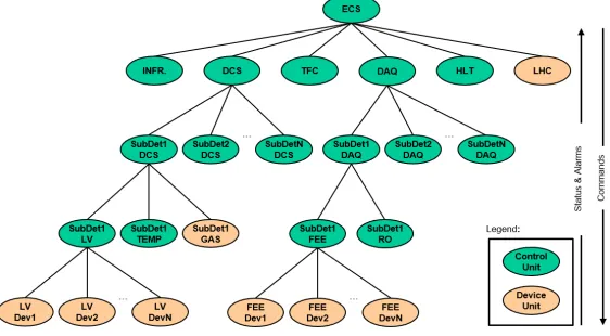
The LHCb ECS is modelled as a tree-like control hierarchy, based on an FSM (Finite State Machine) tree [3]. Commands sent from the top of the hierarchy are propagated all the way down to the leafs which carry on the actions, and the state of the end-nodes at the bottom of the hierarchy is propagated up to the topmost node. At any point one can easily see the state of the entire LHCb experiment, as well as control it from a single place. There are 3 types of nodes which compose the FSM tree:
by the accelerator to a more manageable 1.1 MHz. In the future upgrade of the LHCb ex-periment, the L0 trigger will be removed and the full collision rate will be read out. This will require the upgraded experiment to be able to handle a bandwidth of approximately 4 TBytes/s. To achieve this goal, a new readout system will be implemented with upgraded Timing and Fast ControlandData Acquisitionsystems, as well as upgraded electronics in all the experiment’s sub-detectors. In order to integrate all the new systems and electronics, the LHCb Experiment Control System will also need to be upgraded.
To help with the development of the new systems, a development platform, the MiniDAQ, was created, for which a Control System was developed as a WinCC OA component: the fwMiniDAQ. This component has been developed having in view a future integration of its core developments into the final upgradedLHCb Experiment Control System.
2 The LHCb Experiment Control System
The LHCb ECS incorporates the control for the entire experiment, monitoring and all compo-nents from the infrastructure equipment to the data acquisition itself [2]. The LHCb ECS is a distributed system, based on a commercial SCADA system, WinCC OA, and several custom developed components.
2.1 WinCC OA
WinCC OA is a commercial SCADA software framework which is used in many projects at CERN. It provides several important features for the ECS such as user interfaces, data archiving, alarm-handling in a centrally managed alarm screen as well as interfaces for several different types of equipment using multiple field-buses and protocols. Its open architecture allows for custom developments of the user interfaces, scripts and libraries, and managers and drivers for interfacing, monitoring and controlling custom systems, devices, and electronics. These custom developments can be easily packaged and distributed in order to be installed in other WinCC OA systems in the form ofWinCC OA components.
2.2 Joint Controls Project - JCOP
JCOP is a collaboration between the LHC experiments, the Experimental Physics department and the Industrial Controls group of CERN. JCOP was created in order to join efforts in the integration of the common systems and devices among all experiments. JCOP provides a set of guidelines for component/application development as well as components for common equipment and systems which allows for a greater homogeneity of the different experiment’s control systems and for easier support.
2.3 FSM
The LHCb ECS is modelled as a tree-like control hierarchy, based on an FSM (Finite State Machine) tree [3]. Commands sent from the top of the hierarchy are propagated all the way down to the leafs which carry on the actions, and the state of the end-nodes at the bottom of the hierarchy is propagated up to the topmost node. At any point one can easily see the state of the entire LHCb experiment, as well as control it from a single place. There are 3 types of nodes which compose the FSM tree:
• Control Units - Nodes that logically group other nodes; their state depends on the state of the nodes below; it can be partitioned, i.e. a subtree can be disconnected and taken for independent control;
• Logical Units - Nodes that logically group other nodes; their state depends on the state of the nodes below; they can not be partitioned, but can be enabled/disabled, i.e. in/excluded from control processing;
• Device Units - Nodes that correspond to devices which carry on actions (either real hard-ware devices or softhard-ware processes); their state depends on the real state of the device itself and they can be enabled/disabled;
The LHCb FSM hierarchy, shown in Figure 1, integrates all the detectors and sub-systems, making it possible to control and monitor the entire experiment from a single place. One of the main parts of the ECS is the Run Control, which handles all the tasks that are needed for data taking, such as configuring the sub-detectors front-end electronics and readout boards, the TFC system, the sub-detectors High and Low Voltage (HV/LV) systems, and launching and configuring all the necessary DAQ processes.
Figure 1.LHCb Run Control FSM Hierarchy
2.3.1 FSM Domains
FSM domains are FSM hierarchy branches that group logically related objects. The LHCb FSM Hierarchy has been developed by implementing several domains, such as the DAQ domain (for data acquisition devices), TFC domain (for timing and fast control devices), HLT domain (for the high level trigger system), DCS Domain (for the sub-detector infrastructure devices), HV Domain (for the sub-detector high voltage devices) which are then grouped under a top node, the LHCb Run Control domain. These domains implement FSMs with the states and commands relevant to their specific objects and function.
3 The MiniDAQ System
The LHCb MiniDAQ system has two aspects, a hardware platform and a corresponding software suite controlling and monitoring the hardware.
The hardware basically consists of a CPU server housing a PCIExpress card (the PCIe40). The PCIe40 can be used to interface to the connected electronics and read out the data. In the following sub-sections the different hardware components will be described, together with their corresponding controls components which are aggregated to form the so-called fwMiniDAQcomponent.
3.1 The PCIe40 Card
The PCIe40 is a PCI Express card and is the core component of the upgraded LHCb Online system [4]. It can have up to 48 bi-directional optical links, implementing the GBT protocol [5], running at 4.6 Gbps and can transmit up to 100 Gbps of data through the PCIe lanes. Its core component is a big FPGA (Arria 10) with 1.15 million cells. One of the main advantages of a programmable component on the board is its flexibility. Depending on the firmware loaded into this FPGA, the PCIe40 board can appear in different flavours:
• a readout board (TELL40)
• a readout supervisor (Super ODIN)
• a controls interface (SOL40) to the connected electronics
Because of the large number of logic cells in the FPGA, it is also possible to load the FPGA with a firmware containing all the above functions, although with a reduced number of instantiated links, on a single PCIe40 board. This integrated firmware is called a MiniDAQ firmware and is what is commonly used for the development, together with the MiniDAQ CPU server.
3.1.1 Readout board - TELL40
In the TELL40 flavour the PCIe40 acts as the readout board for the upgraded LHCb detector. Its function is to collect the data from the connected front-end electronics, process these data to form Multi-Event Packets (MEP) as defined by the readout supervisor, and finally send the MEPs, through the PCI Express path, via the hosting CPU server, to the DAQ network for further processing on the online computing farm. It also provides a data buffer for MEPs and is thus capable of absorbing transient network congestion.
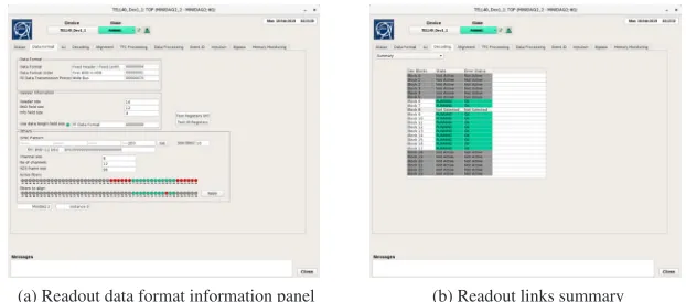
The corresponding component in the fwMiniDAQ framework component provides full monitoring and control for the TELL40 readout board. All the settings and monitoring avail-able in the firmware are implemented and availavail-able from the user interface (as exemplified in Figure 2), which allows for the debugging of the several stages of the data readout. The full 48 data links can be used and monitoring is provided for all of them. It also includes specific features useful for development like buffer memories monitoring and inspection, injection of data, bypass of certain data processing stages and front-end data generation. These features are heavily used at this development stage and are, as such, quickly accessible. In the future some of these features will be moved to an "expert/debugging" section of the user interface. The TELL40 is a generic component used by the whole experiment; however some parts of it need specific sub-detector developments as the data-processing is different for each of the sub-detectors, due to the way each of them reads the data from the front-end electronics. Be-cause of this, the fwMiniDAQ TELL40 control provides some entry points for sub-detector specific user interfaces and the developments of the sub-detector specific blocks
(a) Readout data format information panel (b) Readout links summary
Figure 2.Example of panels from the TELL40 user interface.
3.1.2 Readout supervisor - SODIN
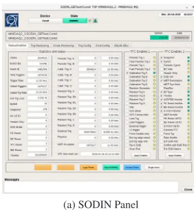
The Super ODIN (SODIN) is the readout supervisor for the experiment. It centrally synchro-nizes and orchestrates the readout of events by distributing the LHC clock and generating clock-synchronous commands and thus managing the dispatching of events [6]. A SODIN is associated with a partition which effectively is a sub-set of readout boards (TELL40) and interface boards (SOL40) operated as an independent entity.
The fwMiniDAQ component provides a SODIN for the MiniDAQ system. It provides a user interface (Figure 3) with all the available configuration parameters for the SODIN, such as trigger settings, timing settings and several counters.
3.1.3 Interface board - SOL40
In its SOL40 flavour the PCIe40 is responsible for interfacing the sub-detectors front-end electronics via the GBT protocol to the TFC and the ECS. It allows the monitoring and control of the front-end electronics via all the available protocols of the new Gigabit Transceiver and Slow Controls Adapter (GBT-SCA) radiation-hard chipset [5] developed at CERN for the upgrade of the LHC experiments. It also interfaces the TFC to the front-end electronics by recovering the clock it receives from SODIN and distributing it to the electronics.
Also the SOL40 has its corresponding component in the fwMiniDAQ suite. The sub-detectors groups can use it to implement their link mappings and verify that the communica-tion and interface from the TFC data to their front-end boards is working correctly and make sure that the devices are ready for data taking.
3.2 Event Writer
This component provides monitoring and control for a simple event writer, which can store the data sent from the readout board through the PCIe lanes on the local hard disk of the host computer. The written data can subsequently be analyzed to study and assess the quality and proper functioning of the entire readout chain.
3.3 fwMiniDAQ FSM Hierarchy
(a) SODIN Panel (b) SOL40 Panel
Figure 3.TFC devices user interfaces.
• DAQ - Includes all the data acquisition devices as the TELL40s and the front-end electron-ics;
• MEP - The event writer;
• TFC - Includes the timing and fast control devices such as a readout supervisor (SODIN) and several SOL40 links;
Figure 4.MiniDAQ Run Control FSM Hierarchy.
The MiniDAQ run control is similar to the global experiment control system run control, in which it allows the full control of the MiniDAQ system from a single place. Sending commands from the top of this FSM hierarchy one can easily configure the whole system and any state change on any of the lower levels of the domains are propagated all the way to the top, allowing to easily detect where the changes come from.
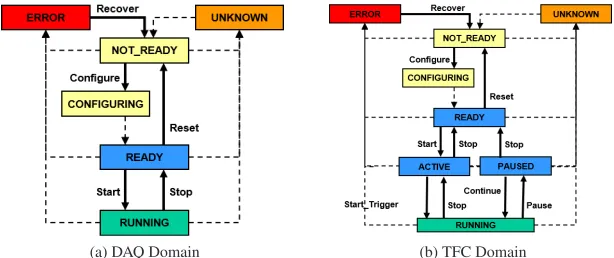
Another feature of the MiniDAQ FSM hierarcy is that the domains that it includes were developed having in mind the final LHCb Global ECS. All the MiniDAQ run control FSM tree control units are instances of these standard domains (Figure 5). These are the same domains that will be used in the global system, which means that all the developments made by the sub-detectors in the corresponding FSM structures are valid without any changes for the global system, which will facilitate the integration. The usage of this FSM hierarchy with standard domains also allowed for the development and integration of a set of features
which are requirements of the global system and the LHCb control system in general, such as SCAN runs where the data acquisition is taken in steps, and between each step it is possible to change the run settings (front-end configurations and readout settings), or the usage of JCOP features, like the recipes which are named sets of configurations used to configure the devices according to specific requirements.
(a) DAQ Domain (b) TFC Domain
Figure 5.FSM Domains provided in the fwMiniDAQ component.
4 Conclusions
The LHCb MiniDAQ provides a fully functional development platform for developing and testing new components for the upgraded LHCb detector. It consists of a hardware platform consisting of a Computer housing a custom PCI Express card and a collection of software components (fwMiniDAQ) covering the necessary control entities to be finally integrated in the LHCb ECS system. It allows for complete stand-alone development and thus facilitates a distributed and de-centralized development of the different detector groups. The components developed by the different detector groups using the provided framework can very easily be integrated into the final LHCb Experiment Control System and will thus facilitate the commissioning of the upgraded detector in 2020/21.
References
[1] The LHCb Collaboration, LHCb Technical Design Report, LHCb-TDR-9, (2009) [2] C. Gaspar and B.Franek, IEEE Transactions on Nuclear Science 53, No.3, 974-979
(2006)
[3] C. Gaspar et al., IEEE Transactions on Nuclear Science51, (2004)
[4] K. Wyillie et al.,Electronics architecture for the LHCb upgrade, LHCb-PUB-2011-011, (2011)
[5] Moreira et al., IOP Journal of Instrumentation5, (2010)
[6] F. Alessio and R. Jacobsson, JINST Topical workshop on electronics for particle physics