Design and implementation of High performance Montgomery
Modular Multiplication on Verilog HDL
1Sukanya Anumala Setty, 2Sai Sravanthi Gandham, 3 Rahamtula shaik
1PG Scholar, Dept of ECE QIS Institute of Technology, Ongole, AP, India. 2Associate Professor, QIS Institute of Technology, Ongole, AP, India. 3Associate Professor, QIS Institute of Technology, Ongole, AP, India.
Abstract
The Montgomery multiplication
algorithm such that the low-cost and
high-performance Montgomery modular
multiplier can be implemented accordingly.
The proposed multiplier receives and
outputs the data with binary representation
and uses only one-level carry-save adder
(CSA) to avoid the carry propagation at
each addition operation. This CSA is also
used to perform operand precomputation
and format conversion from the carry save
format to the binary representation, leading
to a low hardware cost and short critical
path delay at the expense of extra clock
cycles for completing one modular
multiplication. To overcome the weakness, a
configurable CSA (CCSA), which could be
one full-adder or two serial half-adders, is
proposed to reduce the extra clock cycles for
operand precomputation and format
conversion by half. In addition, a
mechanism that can detect and skip the
unnecessary carry-save addition operations
in the one-level CCSA architecture while
maintaining the short critical path
delay is developed.
Index Terms— carry-save addition, low-cost
architecture, Montgomery modular
multiplier, public-key cryptosystem.
I.
Introduction
In many public-key cryptosystems,
modular multiplication (MM) with large
integers is the most critical and
time-consuming operation. Therefore, numerous
algorithms and hardware implementation
have been presented to carry out the MM
more quickly, and Montgomery’s algorithm
is one of the most well-known MM
algorithms. Montgomery’s algorithm [4]
determines the quotient only depending on
the least significant digit of operands and
replaces the complicated division in
conventional MM with a series of shifting
modular additions to produce S = A × B ×
R−1 (mod N), where N is the k-bit modulus, R−1 is the inverse of R modulo N, and R =
implemented into VLSI circuits to speed up
the encryption / decryption process.
However, the three-operand addition in the
iteration loop of Montgomery’s algorithm as
shown in step 4 of Fig. 1 requires long carry
propagation for large operands in binary
representation. To solve this problem,
several approaches
Fig. 1. MM algorithm.
based on carry-save addition were proposed
to achieve a significant speedup of
Montgomery MM. Based on the
representation of input and output operands,
these approaches can be roughly divided
into semi-carry-save (SCS) strategy and full
carry-save (FCS) strategy. In the SCS
strategy, the input and output operands (i.e.,
A, B, N, and S) of the Montgomery MM are
represented in binary, but intermediate
results of shifting modular additions are kept
in the carry-save format to avoid the carry
propagation. However, the format
conversion from the carry-save format of the
final modular product into its binary
representation is needed at the end of each
MM.
This conversion can be accomplished
by an extra carry propagation adder (CPA)
or reusing the carry-save adder (CSA)
architecture [8] iteratively. Contrary to the
SCS strategy, the FCS strategy maintains
the input and output operands A, B, and S in
the carry-save format, denoted as (AS, AC),
(BS, BC), and (SS, SC), respectively, to
avoid the format conversion, leading to
fewer clock cycles for completing a MM.
Nevertheless, this strategy implies that the
number of operands will increase and that
more CSAs and registers for dealing with
these operands are required. Therefore, the
FCS-based Montgomery modular
multipliers possibly have higher hardware
complexity and longer critical path than the
SCS-based multipliers. Kuang et al. [10]
have proposed an energy-efficient
FCS-based multiplier (denoted as FCS-MMM42
multiplier) in which the superfluous
operations of the four-to-two (two-level)
CSA architecture are suppressed to reduce
the energy dissipation and enhance the
multiplier still suffers from the high area
complexity and long critical path delay.
Other techniques, such as parallelization,
high-radix algorithm, and systolic array
design, can be combined with the CSA
architecture to further enhance the
performance of Montgomery multipliers.
However, these techniques probably cause a
large increase in hardware complexity and
power/energy dissipation, which is
undesirable for portable systems with
constrained resources. Accordingly, this
paper aims at enhancing the performance of
CSA-based Montgomery multiplier while
maintaining low hardware complexity.
Instead of the FCS-based multiplier with
two-level CSA architecture in, a new
SCS-based Montgomery MM algorithm and its
corresponding hardware architecture with
only one-level CSA are proposed in this
paper. The proposed algorithm and hardware
architecture have the following several
advantages and novel contributions over
previous designs. First, the one-level CSA is
utilized to perform not only the addition
operations in the iteration loop of
Montgomery’s algorithm but also B + N and
the format conversion, leading to a very
short critical path and lower hardware cost.
However, a lot of extra clock cycles are
required to carry out B + N and the format
conversion via the one-level CSA
architecture. Therefore, the benefit of short
critical path will be lessened. To overcome
the weakness, we then modify the one-level
CSA architecture to be able to perform one
three-input carry-save addition or two serial
two-input carry-save additions, so that the
extra clock cycles for B + N and the format
conversion can be reduced by half. Finally,
the condition and detection circuit, which
are different with that of FCS-MMM42
multiplier, are developed to precompute
quotients and skip the unnecessary
carry-save addition operations in the one-level
configurable CSA (CCSA) architecture
while keeping a short critical path delay.
Therefore, the required clock cycles for
completing one MM operation can be
significantly reduced.
II. Montgomery Multiplication
In this section, we propose a newSCS-based Montgomery MM algorithm to
reduce the critical path delay of
Montgomery multiplier. In addition, the
drawback of more clock cycles for
completing one multiplication is also
improved while maintaining the advantages
complexity. A. Critical Path Delay
Reduction The critical path delay of
SCS-based multiplier can be reduced by
combining the advantages of FCS-MM-2
and SCS-MM-2. Fig. 7 shows the modified
SCS-based Montgomery multiplication
(MSCS-MM) algorithm and one possible
hardware architecture, respectively. The
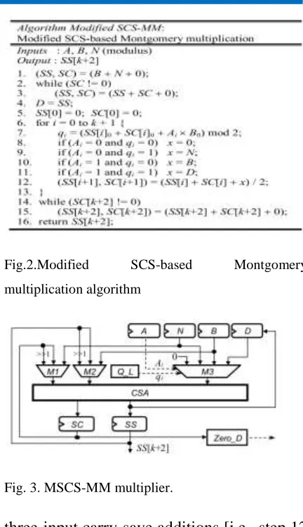
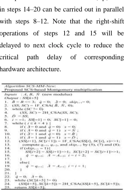
Zero_D circuit in Fig. 7 is used to detect
whether SC is equal to zero, which can be
accomplished using one NOR operation.
The Q_L circuit decides the qi value
according to step 7 of Fig. 2. The carry
propagation addition operations of B + N
and the format conversion are performed by
the one-level CSA architecture of the
MSCS-MM multiplier through repeatedly
executing the carry-save addition (SS, SC) =
SS + SC + 0 until SC = 0. In addition, we
also precompute Ai and qi in iteration i−1
(this will be explained more clearly in
Section III-C) so that they can be used to
immediately select the desired input operand
from 0, N, B, and D through the multiplexer
M3 in iteration i. Therefore, the critical path
delay of the MSCS-MM multiplier can be
reduced into TMUX4 + TFA.
Fig.2.Modified SCS-based Montgomery
multiplication algorithm
Fig. 3. MSCS-MM multiplier.
three-input carry-save additions [i.e., step 12
of Fig. 2(a)] k + 2 times, many extra clock
cycles are required to perform B + N and the
format conversion via the one-level CSA
architecture because they must be performed
once in every MM. Furthermore, the extra
clock cycles for performing B+N and the
format conversion through repeatedly
executing the carry-save addition (SS, SC) =
SS +SC +0 are dependent on the longest
carry propagation chain in SS + SC. If SS =
one-level CSA architecture needs k clock cycles
to complete SS + SC.
Fig.4. Conventional FA circuit
Fig.5. Existing CFA circuit.
That is, 3k clock cycles in the worst
case are required for completing one MM.
Thus, it is critical to reduce the required
clock cycles of the MSCS-MM multiplier.
B. Clock Cycle Number Reduction To
decrease the clock cycle number, a CCSA
architecture which can perform one
three-input carry-save addition or two serial
two-input carry-save additions is proposed to
substitute for the one-level CSA architecture
in Fig. 2. Fig. 5 shows two cells of the
one-level CSA architecture in Fig. 3., each cell is
one conventional FA which can perform the
three-input carry-save addition. Fig. 5 shows
two cells of the proposed configurable FA
(CFA) circuit. If α = 1, CFA is one FA and
can perform one three-input carry-save
addition (denoted as 1F_CSA). Otherwise, it
is two half-adders (HAs) and can perform
two serial two-input carry-save additions
(denoted as 2H_CSA), as shown. In this
case, G1 of CFAj and G2 of CFAj+1 in Fig.
5 will act as HA1 j , and G3, G4, and G5 of
CFAj in Fig. 5 will behave as HA2 j
Moreover, we modify the 4-to-1 multiplexer
M3 in Fig. into a simplified multiplier SM3
.because one of its inputs is zero, where ∼
denotes the INVERT operation. Note that
M3 has been replacedby SM3 in the
proposed one-level CCSA architecture.
According to the delay ratio shown
In addition, we also skip the
unnecessary operations in the for loop (steps
6 to 13) of Fig. 2 to further decrease the
clock cycles for completing one
Montgomery MM. The crucial computation
in the for loop of Fig. 7(a) is performing the
following three-to-two carry-save addition:
(SS[i + 1], SC[i + 1]) = (SS[i] + SC[i] + x)/2
D depending on the values of Ai and qi .
The computation process of (1) is shown in
Fig. 9. When Ai = 0 and qi = 0, x is equal to
0 and SS[i]0 must be equal to SC[i]0
because the sum of SS[i]0 + SC[i]0 + x0 is
equal to 0. That is, if Ai = 0 and qi = 0, then
SS[i]0 = SC[i]0. Based on this observation,
we can conclude that the sum of the carry
propagation addition SS[i +1]k+1:0 + SC[i +
1]k+1:0 is equal to the sum of the carry
propagation addition SS[i]k+1:1 +
SC[i]k+1:1 when Ai = qi = 0 and SS[i]0 =
SC[i]0 = 0. As a result, the computation of
(1) in iteration i can be skipped if we
directly right shift the outputs of one-level
CSA architecture in the (i − 1)th iteration by
two bit positions (i.e., divided by 4) instead
of one bit position (i.e., divided by 2) when
Ai = qi = 0 and SS[i]0 = SC[i]0 = 0.
Accordingly, the signal skipi+1 used in the
ith iteration to indicate whether the
carry-save addition in the (i + 1)th iteration will be
skipped can be expressed as skipi+1 =
∼(Ai+1 ∨ qi+1 ∨ SS[i + 1]0) (2) where ∨
represents the OR operation.
III.
Proposed
Algorithm
and
Hardware Architecture
On the bases of critical path delay
reduction, clock cycle number reduction,
and quotient precomputation mentioned
above, a new SCS-based Montgomery MM
algorithm (i.e., SCS-MM-New algorithm
shown in Fig.6) using one-level CCSA
architecture is proposed to significantly
reduce the required clock cycles for
completing one MM. As shown in
SCS-MM-New algorithm, steps 1–5 for
producing Bˆ and Dˆ are first performed.
Note that because qi+1 and qi+2 must be
generated in the ith iteration, the iterative
index i of Montgomery MM will start from
−1 instead of 0 and the corresponding initial values of qˆ and Aˆ must be set to 0.
Furthermore, the original for loop is
replaced with the while loop in
SCS-MM-New algorithm to skip some unnecessary
iterations when skipi+1 = 1. In addition, the
ending number of iterations in
SCS-MM-New algorithm is changed to k + 4 instead
of k + 1 . This is because B is replaced with
Bˆ and thus three extra iterations for
computing division by two are necessary to
ensure the correctness of Montgomery MM.
In the while loop, steps 8–12 will be
performed in the proposed one-level CCSA
architecture with one 4-to-1 multiplexer.
in step 13 and the selections of Aˆ, qˆ, and i
in steps 14–20 can be carried out in parallel
with steps 8–12. Note that the right-shift
operations of steps 12 and 15 will be
delayed to next clock cycle to reduce the
critical path delay of corresponding
hardware architecture.
Fig. 6. SCS-MM-New algorithm.
multiplier SM3, one skip detector Skip_D,
one zero detector Zero_D, and six registers.
Skip_D is developed to generate skipi+1, qˆ, and Aˆ in the ith iteration. Both M4 and M5
in Fig. 11 are 3-bit 2-to-1 multiplexers and
they are much smaller than k-bit
multiplexers M1, M2, and SM3.
Fig. 7. SCS-MM-New multiplier.
Fig. 8. Skip detector Skip_D
In addition, the area of Skip_D is
negligible when compared with that of the
k-bit one-level CCSA architecture. Similar
to Fig. 4, the select signals of multiplexers
M1 and M2 in Fig. 11 are generated by the
control part, which are not depicted for the
sake of simplicity. Fig. 12. Skip detector
Skip_D. At the beginning of Montgomery
multiplication, the FFs stored skipi+1, qˆ, Aˆ
are first reset to 0 as shown in step 1 of
SCS-MM-New algorithm so that Dˆ = Bˆ
+Nˆ can be computed via the one-level
while loop, the skip detector Skip_D shown
in Fig. 12 is used to produce skipi+1, qˆ, and Aˆ. The Skip_D is composed of four XOR
gates, three AND gates, one NOR gate, and
two 2-to-1 multiplexers. It first generates the
qi+1, qi+2, and skipi+1 signal in the ith
iteration according to (5), (7), and (8),
respectively, and then selects the correct qˆ and Aˆ according to skipi+1. At the end of the ith iteration, qˆ, Aˆ, and skipi+1 must be
stored to FFs.
Fig.9. Proposed CCSA architecture.
In the next clock cycle of the ith iteration,
SM3 outputs a proper x according to qˆ and Aˆ generated in the ith iteration as shown in
steps 8–11, and M1 and M2 output the
correct SC and SS according to skipi+1
generated in the ith iteration. That is, the
right-shift 1-bit operations in steps 12 and
15 of SCS-MM-New algorithm are
performed together in the next clock cycle
of iteration i. In addition, M4 and M5 also
select and output the correct SC[i]2:0 and
SS[i]2:0 according to skipi+1 generated in
the ith iteration. Note that SC[i]2:0 and
SS[i]2:0 can also be obtained from M1 and
M2 but a longer delay is required because
they are 4-to-1 multiplexers. After the while
loop in steps 7–21 is completed, qˆ and Aˆ
stored in FFs are reset to 0. Then, the format
conversion in steps 23 and 24 can be
performed by the SCS-MM-New multiplier
similar to the computation of Dˆ = Bˆ + Nˆ
in steps 3 and 4. Finally, SS[k + 5] in binary
format is outputted when SC[k + 5] is equal
to 0.
Existing Proposed
Delay 1158.613ns 1150550ns
Fig. 10. Results
IV. Simulation and Synthesize
Results
Fig. 11. Simulation Wave Forms
Existing Proposed
No.of Slices 3160 3147
No.of Slice Flip Flops 68 65
No. of bonded IOBs 41 39
Fig. 12. Synthesize Report
V. Conclusion
FCS-based multipliers keep up the info
and yield operands of the Montgomery MM
in the convey spare organization to escape
from the arrangement change, prompting
less clock cycles however bigger territory
than SCS-based multiplier. To improve the
execution of Montgomery MM while
keeping up the low equipment many-sided
quality, this paper has changed the
SCS-based Montgomery increase calculation and
professional represented a minimal effort
and elite Montgomery secluded multiplier.
The proposed multiplier utilized one-level
CCSA design and skirted the superfluous
convey spare addition operations to a great
extent diminish the basic way delay and
required clock cycles for finishing one MM
operation. Trial comes about demonstrated
that the proposed approaches are in fact fit
for upgrading the execution of radix-2
CSA-based Montgomery multiplier while
keeping up low equipment many-sided
quality.
VI. References
[1] R. L. Rivest, A. Shamir, and L.
Adleman, “A method for obtaining digital
signatures and public-key cryptosystems,”
Commun. ACM, vol. 21, no. 2, pp. 120–126,
Feb. 1978.
[2] V. S. Miller, “Use of elliptic curves in
cryptography,” in Advances in Cryptology.
Berlin, Germany:Springer-Verlag,1986, pp.
417–426.
[3] N. Koblitz, “Elliptic curve cryptosystems,” Math. Comput., vol. 48,
no. 177, pp. 203–209, 1987.
[4] P. L. Montgomery, “Modular multiplication without trial division,” Math.
Comput., vol. 44, no. 170, pp. 519–521, Apr.
1985.
[5] Y. S. Kim, W. S. Kang, and J. R. Choi,
“Asynchronous implementation
of 1024-bit modular processor for RSA
cryptosystem,” in Proc. 2nd IEEE
Asia-Pacific Conf. ASIC, Aug. 2000, pp. 187–
190.
[6] V. Bunimov, M. Schimmler, and B.
Tolg, “A complexity-effective version of Montgomery’ s algorihm,” in Proc.
Workshop Complex. Effective Designs, May
[7] H. Zhengbing, R. M. Al Shboul, and V.
P. Shirochin, “An efficient architecture of
1024-bits cryptoprocessor for RSA
cryptosystem based on modified
Montgomery’s algorithm,” in Proc. 4th
IEEE Int. Workshop Intell. Data Acquisition
Adv. Comput. Syst., Sep. 2007, pp. 643–646.
[8] Y.-Y. Zhang, Z. Li, L. Yang, and S.-W.
Zhang, “An efficient CSA architecture for Montgomery modular multiplication,”
Microprocessors Microsyst., vol. 31, no. 7,
pp. 456–459, Nov. 2007.
[9] C. McIvor, M. McLoone, and J. V.
McCanny, “Modified Montgomery modular
multiplication and RSA exponentiation
techniques,” IEE Proc.- Comput. Digit.
Techn., vol. 151, no. 6, pp. 402–408, Nov.
2004.
Authors Details
Sukanya Anumala Setty has
completed her B.Tech in
Electronics and
Communication Engineering
from QIS Institute of Technology in
2016,JNTUK affiliated college. She is
pursuing her M.Tech in VLSI and
Embedded Systems from QIS
Institute of Technology, JNTUK
affiliated college.
Sai Sravanthi Gandham is an Associate
Professor at QIS Institute of Technology,
Ongole. She received her B.Tech in
Electronics and Communication
Engineering from QIS College of
Engineering and Technology, Ongole
affiliated to JNTUK, M.Tech, in Digital
Electronics Communication System from St.
Ann’s college of Engineering and
Technology, Chirala affiliated to JNTUK.
Mr. Shaik. Rahamtula is
currently working as Associate
Professor in ECE Department,
QIS Institute of technology,
Ongole, A.P, India. He received his B. Tech
degree in the department of Electronics and
Communication Engineering, from KMCET
(Affiliated to JNTU Hyderabad). He
received his M. Tech from QIS college of
Engineering and Technology (Affiliated to
JNTU Kakinada). His research interests in
the area of Face recognition, Content based
image retrieval, Image compression, VLSI,