VLSI IMPLEMENTATION OF AN EFFICIENT CARRY
SELECT ADDER ARCHITECTURE
Senthilkumar.A
1, Kousalya devi.A
2 1Assistant Professor (SS), EEE Dept, Dr. Mahalingam College of Engineering & Technology, Pollachi,
2PG Scholar, Dr. Mahalingam College of Engineering and Technology, Pollachi,
ABSTRACT
Adders are one of the widely used digital components in digital integrated circuit design. Carry select adder
(CSLA) is known to be the fastest adder among the conventional adder structures. Due to the rapidly growing
mobile industry not only the faster arithmetic unit but also less area and low power arithmetic units are needed.
Carry-select method has deemed to be a good compromise between cost and performance in carry propagation
adder design. However, conventional carry-select adder (CSLA) is still area-consuming due to the dual ripple
carry adder structure. The modified CSLA architecture has developed using Binary to Excess-1 converter
(BEC). This paper proposes an efficient method by modifying the gates in the BEC design. This work uses a
simple and efficient gate-level modification to significantly reduce the area and power of the CSLA. Based on
this modification 8-bit and 16-bit CSLA architecture have been developed and compared with the regular CSLA
architecture. This work evaluates the performance of the proposed designs in terms of area and power. The
results analysis shows that the proposed CSLA structure is better than the conventional CSLA. This work proves
that carry select adder using binary to excess 1 converter is efficient for VLSI implementation.
Keywords: CSLA, Binary to Excess- 1, Low Power, Area Efficient
I INTRODUCTION
Adders are commonly found in the critical path of many building blocks of microprocessors and digital signal
processing chips. Adders are essential not only for addition, but also for subtraction, multiplication, and
division. Addition is one of the fundamental arithmetic operations. A fast and accurate operation of a digital
system is greatly influenced by the performance of the resident adders. The most important for measuring the
quality of adder designs in the past were propagation delay, and area. The three most widely accepted metrics
for measuring the Performance of a circuit are power, delay and area. Minimizing Area and delay has always
been considered important, but Reducing power consumption has been gaining prominence Recently with the
increasing level of device integration and the Growth in complexity of micro-electronic circuits, reduction of
in electronic Circuits, only recently has it become a limiting factor for a broad Range of applications, thereby
requiring consideration early on in the design process.
Carry Select Adder is one of the fastest adders used in many data-processing processors to perform fast
arithmetic functions. It alleviates the problem of carry propagation delay by independently generating multiple
carries and then selects a carry to generate the sum (3).The carry-select adder (CSLA) provides a compromise
between small area but longer delay ripple carry adder (RCA) and larger area with shorter delay carry
look-ahead adder (6). CSLA uses multiple pairs of ripple carry adder (RCA) to generate partial sum and carry by
considering carry input Cin=0 and Cin=1, then the final sum and carry are selected by multiplexers (MUX) (6).
The modified CSLA using BEC has reduced area and power consumption with slight increase in delay(2, 4, 5).
BEC design consists of AND, XOR and NOT gates as its structure. In this structure the XOR gate will be
replaced by MUX with NOT gate. The proposed CSLA design reduces the area and power by replacing the
gates in BEC design..
This paper is organized as follows; section II explains the conventional carry select adder. The modified and
proposed CSLA are presented in Section III and section IV respectively. Section V deals with the result
obtained. Section VI concludes the paper.
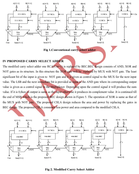
II CONVENTIONAL CARRY SELECT ADDER
Addition is basic operation used in many data path logic systems such as Adders, Multipliers etc. Carry select
adders are used for high speed operation by reducing the Carry propagation delay. The basic operation of Carry
Select Adder (CSLA) is Parallel Computation. The carry-select adder (CSLA) provides a compromise between
small area but longer delay ripple carry adder (RCA) and larger area with shorter delay carry look-ahead adder .
CSLA uses multiple pairs of ripple carry adder (RCA) to generate partial sum and carry by considering carry
input Cin=0 and Cin=1, then the final sum and carry are selected by multiplexers (MUX).The conventional
carry select adder is shown in fig 1.
III MODIFIEDCARRY SELECT ADDER
The modified carry select adder is to use BEC instead of the RCA with Cin = 1 in order to reduce the area and
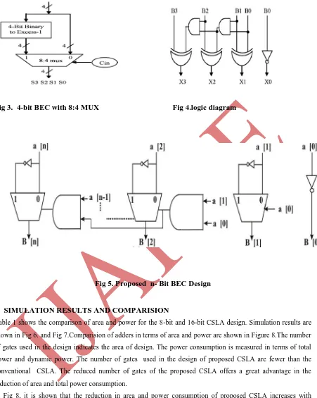
power consumption of the regular CSLA. To replace the n-bit RCA, an n+1-bit BEC is required. BEC together
with a multiplexer (MUX) is described in Fig 3,one input of the 8:4 MUX gets as it input (B3, B2, B1, and B0)
and another input of the MUX is the BEC output. This produces the two possible partial product results in
parallel and the muxes are used to select either BEC output or the direct inputs according to the control signal
Cin. The Boolean expressions of 4-bit BEC are listed below, (Note: functional symbols, ~ NOT, & AND, ^
XOR).The logic diagram of 4-bit BEC is shown in Fig 4.
X0 = ~ B0
X1 = B0 ^ B1
X2 = B2 ^ (B0 & B1)
X3 = B3 ^ (B0 & B1 & B2)
The modified carry select adder is shown in Figure 2.The least significant bits are added using conventional
block receives the two sets of input and selects the final sum based on the select input from the previous stage.
One input of the 8:4 multiplexer gets as its input B3, B2, B1, and B0 and another input of the multiplexer is the
BEC output. Use of BEC with multiplexer thus achieves fast incrementing action with reduced gate count. Thus,
the modified CSLA is better than the conventional CSLA circuit in terms of area and power.
Fig 1.Conventional carry select adder
IV PROPOSED CARRY SELECT ADDER
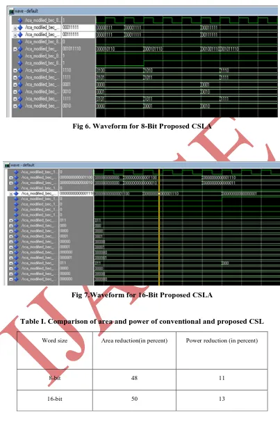
The modified carry select adder one RCA(Cin=1) is replaced by BEC.BEC design consists of AND, XOR and
NOT gates as its structure. In this structure the XOR gate will be replaced by MUX with NOT gate. The least
significant bit of the input is given to NOT gate and it is given as control signal to the MUX for the next input
value. The LSB and the next immediate bit is provided as input to the AND gate where its corresponding output
value is given as a control signal to the Multiplexer. Depending upon the control signal it will produce the sum
value. If it is 0,then its output is same as the input otherwise it produces its complement value .It is continued till
the end of MSB which is the proposed BEC design shown in Figure 5. The operation of XOR is same as that of
the MUX with NOT gate. The proposed CSLA design reduces the area and power by replacing the gates in
BEC design. The proposed CSLA consumes less power and area compared to the modified CSLA.
Fig 3. 4-bit BEC with 8:4 MUX Fig 4.logic diagram
Fig 5. Proposed n- Bit BEC Design
V SIMULATION RESULTS AND COMPARISION
Table 1 shows the comparison of area and power for the 8-bit and 16-bit CSLA design. Simulation results are
shown in Fig 6. and Fig 7.Comparision of adders in terms of area and power are shown in Figure 8.The number
of gates used in the design indicates the area of design. The power consumption is measured in terms of total
power and dynamic power. The number of gates used in the design of proposed CSLA are fewer than the
conventional CSLA. The reduced number of gates of the proposed CSLA offers a great advantage in the
reduction of area and total power consumption.
In Fig 8, it is shown that the reduction in area and power consumption of proposed CSLA increases with
increasing word size of adder. It is clear from above results that the area of 8-bit and16-bit proposed CSLA is
reduced by 48% and 50%. The total power consumed shows the similar pattern of increasing reduction in power
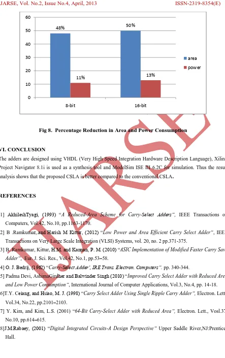
Fig 6. Waveform for 8-Bit Proposed CSLA
Fig 7.Waveform for 16-Bit Proposed CSLA
Table I. Comparison of area and power of conventional and proposed CSL
Word size Area reduction(in percent) Power reduction (in percent)
8-bit 48 11
Fig 8. Percentage Reduction in Area and Power Consumption
VI. CONCLUSION
The adders are designed using VHDL (Very High Speed Integration Hardware Description Language), Xilinx
Project Navigator 8.1i is used as a synthesis tool and ModelSim ISE III 6.2C for simulation. Thus the result
analysis shows that the proposed CSLA is better compared to the conventional CSLA
.
REFERENCES
[1] AkhileshTyagi, (1993) “A Reduced-Area Scheme for Carry-Select Adders”, IEEE Transactions on
Computers, Vol.42, No.10, pp.1163-1170.
[2] B .Ramkumar,.and Harish M Kittur, (2012) “Low Power and Area Efficient Carry Select Adder”, IEEE
Transactions on Very Large Scale Integration (VLSI) Systems, vol. 20, no. 2 pp.371-375.
[3] B. Ramkumar, Kittur, H.M. and Kannan, P. M. (2010) “ASIC Implementation of Modified Faster Carry Save
Adder”, Eur. J. Sci. Res., Vol.42, No.1, pp.53–58.
[4] O. J. Bedrij, (1962) “Carry-Select Adder’, IRE Trans. Electron. Computers”. pp. 340-344.
[5] Padma Devi, AshimaGirdher and Balwinder Singh (2010) “Improved Carry Select Adder with Reduced Area
and Low Power Consumption”, International Journal of Computer Applications, Vol.3, No.4, pp. 14-18.
[6]T.Y. Ceiang, and Hsiao, M. J. (1998) “Carry Select Adder Using Single Ripple Carry Adder”, Electron. Lett.,
Vol.34, No.22, pp.2101–2103.
[7] Y. Kim, and Kim, L.S. (2001) “64-Bit Carry-Select Adder with Reduced Area”, Electron. Lett., Vosl.37,
No.10, pp.614–615.
[8]J.M.Rabaey, (2001) “Digital Integrated Circuits-A Design Perspective” Upper Saddle
River,NJ:Prentice-Hall.
48% 50%
11% 13%
0 10 20 30 40 50 60
8-bit 16-bit
area