Structural, morphology and optical properties of Zn
(1−x)Cd
xO solid solution
grown on c-plane sapphire substrate
A. Fouzri1,a, M. A. Boukadhaba2, M. Oumezzine2, A. Bchetnia3 and V. Sallet4
1Laboratoire Physico-chimie des Matériaux, Unité de Service Commun de Recherche « High resolution X-ray diffractometer »,
Département de Physique, Université de Monastir, Faculté des Sciences de Monastir, Avenue de l’Environnement, 5019 Monastir, Tunisia.
2Laboratoire Physico-chimie des Matériaux, Département de Physique, Université de Monastir, Faculté des Sciences de Monastir,
Avenue de l’Environnement, 5019 Monastir, Tunisia.
3Unité de recherche hétéroepitaxie et ses applications, Département de Physique, Université de Monastir, Faculté des Sciences de
Monastir, Avenue de l’Environnement, 5019 Monastir, Tunisia.
4Groupe d’Etude de la Matière Condensée, Centre National de la Recherche Scientifique/Université de Versailles Saint Quentin en
Yvelines,UMR 8635, Paris France.
Abstract. Zn(1-x)CdxO solid solutions with a composition ranging from pure ZnO up to x=0.046 have been grown on c-plane sapphire substrates by using metal organic chemical vapor deposition (MO-CVD). The lattice deformation, morphology and optical properties of these films were examined in detail using high resolution X-ray diffraction, atomic force microscopy (AFM) and photoluminescence (PL) as Cd incorporation. Our study reveals significant microstructure modification of Zn(1-x)CdxO from x≥0.7% but single phase of wurtzite structure is maintained for all films. The Pl spectra
and the band gap of the Zn(1-x)CdxO film show red shift to visible light range which is interpreted in terms of band gap modulation due to Cd incorporation. Increase of Cd content leads to the emission broadening with growing lower energy peak (at 10K) and degraded crystallinity.
1 Introduction
ZnO is a II-VI wide band gap (3.3 eV) semiconductor material and has an ability to modulate the band to lower level by alloying with CdO [1]. ZnO has a wurtzite structure (a=3.25 Å, c=5.21 Å). CdO has rock salt (RS) structure (a=4.70 Å). The choice of CdO is
based on the fact that ionic radius of Cd2+ (0.95Å) is close to that of Zn2+ (0.74Å), that is, wurtzite phase alloy can be expected in
spite of RS structure of CdO. The thermodynamic solubility limit of CdO in ZnO has been reported to be less 2 mol% according to
the phase diagram of the ZnO-CdO-P2O5 ternery system [2]. Although good results have been reported for homoepitaxially grown
ZnO film [3], the high cost and limited availability of high-quality bulk ZnO substrates preclude their use in mass production environments. On the contrary, sapphire has been chosen as a substrate material due to its relatively low cost, availability in large area wafers. Many studies on the growth of ZnO films have used c-plane sapphire as substrate [4-11]. However, the heteroepitaxy of ZnO on sapphire presents several problems due to differences in their chemical nature, structure and lattices parameters [12]. Furthermore, it is known that the properties of thin solid film are closely related to its microstructure, morphology and surface roughness.
In our work, we are using optical transmission measurements to estimated cadmium incorporation, high-resolution X-ray diffraction (HRXRD), atomic force microscopy (AFM) and photoluminescence to analyses the structural, morphology and optical properties of Zn(1−x)CdxO solid solutions grown, by metal organic chemical vapor deposition (MO-CVD), on c-plane sapphire substrate as Cd
incorporation.
a
e-mail : [email protected]
DOI: 10.1051/ C
Owned by the authors, published by EDP Sciences, 2012 epjconf 20122/ 900019
2 Experiments
The layer is grown in horizontal MO-CVD reactor at atmospheric pressure under N Cadmium (DMCd) and tertiary butanol
(ter-of 380° C. The growth conditions are described elsewhere [13]. With similar growth directly deposited on c-plane sapphire substrates from Crystec.
rate of DMZn was maintained constant while th
series of five samples with different compositions are listed in table 1.
Table 1. MO-CVD growth parameters, energy band gap (E
Thickness of ZnCdO film deposited on c-plane sapphire substrate for the different flux ratios used respectively about 1 µm, 0.6 µm, 2.2 µm, 1.6 µm and 1.4 µm which are measured
clearly show the non-uniformity of layers thickness.
Fig. 1. Cross section SEM images of
These samples are characterized by optical transmission measurements at 300K, in the range spectrophotometer which can return either the absorption coefficient in arbitrary units or the trans
shows the square (αE) for the Zn(1−x)CdxO solid solution deposited on c
E. The absorption band-edge energy of these samples
Zn(1−x)CdxO films shows shrinkage in energy gap, which provides supportive evidence that Cd incorporates in ZnO. The cadmium
contents (table 1) in these layers deposited established by T. Makino et al. [14], where
reached is 4.6% which is over twice larger than the thermodynamic solubility limit.
Sample DEZn Pressure (Pa)
M1 13
M2 26
M3 26
M4 26
M5 26
CVD reactor at atmospheric pressure under N2 carrier gas. Diethyl
-butanol) are used as Zn, Cd and oxygen precursors, respectively at a growth temperature of 380° C. The growth conditions are described elsewhere [13]. With similar growth parameters, thin films of Zn
plane sapphire substrates from Crystec. In order to obtain different compositions of cadmium, the molar flow rate of DMZn was maintained constant while that of DECd was gradually increased from 1 to 10 cc.
series of five samples with different compositions are listed in table 1.
CVD growth parameters, energy band gap (Eg) and cadmium content at % of Zn(1-x)Cdx0 solid solutions deposited on c plane sapphire substrate.
plane sapphire substrate for the different flux ratios used
respectively about 1 µm, 0.6 µm, 2.2 µm, 1.6 µm and 1.4 µm which are measured from cross-section SEM images (F uniformity of layers thickness.
Cross section SEM images of Zn(1-x)CdxO deposited on c-plane sapphire substrates for
re characterized by optical transmission measurements at 300K, in the range spectrophotometer which can return either the absorption coefficient in arbitrary units or the trans
O solid solution deposited on c-plane sapphire substrate as a function of the photon energy edge energy of these samples is estimated by extrapolating linear part of (
shows shrinkage in energy gap, which provides supportive evidence that Cd incorporates in ZnO. The cadmium deposited on c-plane sapphire substrate are determined from energy band gap (E
where we have used Eg(x=0) deduced from reference sample
reached is 4.6% which is over twice larger than the thermodynamic solubility limit.
DEZn Pressure (Pa) DMCd Pressure (Pa) Eg(eV)
13 0 3.26
26 1.5 3.24
26 2.5 3.23
26 5 3.14
26 10 3.07
carrier gas. Diethyl-Zinc (DEZn), Dimethyl-butanol) are used as Zn, Cd and oxygen precursors, respectively at a growth temperature
parameters, thin films of Zn(1−x)CdxO are
In order to obtain different compositions of cadmium, the molar flow rom 1 to 10 cc. The growth parameters of a
0 solid solutions deposited on
c-plane sapphire substrate for the different flux ratios used (0, 1, 2.5, 5 and 10 cc) are section SEM images (Figure 1). They
plane sapphire substrates for the different flux ratios used.
re characterized by optical transmission measurements at 300K, in the range 310 – 690 nm using a DR/4000U spectrophotometer which can return either the absorption coefficient in arbitrary units or the transmittance in percentage. Figure 2 plane sapphire substrate as a function of the photon energy
estimated by extrapolating linear part of (αE)2 to zero. As seen here, the
shows shrinkage in energy gap, which provides supportive evidence that Cd incorporates in ZnO. The cadmium
are determined from energy band gap (Eg) equation
reference sample M1. The highest Cd content
(eV) x (%)
3.26 0
3.24 0.5
3.23 0.7
3.14 3
1.8 2.0 2.2 2.4 2.6 2.8 3.0 3.2 3.4 3.6 3.8 4.0 Eg=3,26eV E (eV) ( α α α α E ) 2(a .u )
ZnO/c-plane sapphire (0 cc)
1.8 2.0 2.2 2.4 2.6 2.8 3.0 3.2 3.4 3.6 3.8 4.0
Eg=3,24 eV E (eV) ( α α α α E ) 2(a .u )
ZnCdO/c-plane sapphire (1 cc)
1.8 2.0 2.2 2.4 2.6 2.8 3.0 3.2 3.4 3.6 3.8 4.0
Eg=3,23 eV E (eV) (α αα α E ) 2(a .u )
ZnCdO/c-plane sapphire (2.5 cc)
1.8 2.0 2.2 2.4 2.6 2.8 3.0 3.2 3.4 3.6 3.8 4.0
ZnCdO/c-plane sapphire (5 cc)
Eg=3,14 eV E (eV) ( α α α α E ) 2(a .u )
1.8 2.0 2.2 2.4 2.6 2.8 3.0 3.2 3.4 3.6 3.8 4.0
Eg=3,07 eV E (eV) ( α α α α E ) 2(a .u )
ZnCdO/c-plane sapphire (10 cc)
Fig. 2. Plots of the square (αE) as a function of photon energy (E) for the Zn(1-x)CdxO solid solution deposited on c-plane
sapphire substrate for the different flux ratios used.
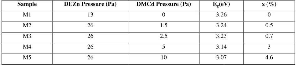
High-resolution X-ray diffraction (HRXRD) experiments were performed with D8 discover Bruker AXS diffractometer using CuKα1
radiation at 1.5406 Å. The 2θ-θ scan revealed that all the films had c-axis orientation and wurtzite phase. No indication of any
rocksalt phase related to segregate CdO within the layers could be detected. For illustration, XRD measurements of ZnO and Zn(1-x)CdxO (x=4.6%) grown on c-plane sapphire are represented in Figure 3. In addition to the ZnO (0002) reflexion and its
harmonic, we observe (0006) and (00012) reflexion corresponding to c-plane sapphire substrate.
30 40 50 60 70 80 90
I (a .u ) I (a .u )
ZnO/c-plane sapphire (x=0%)
2θ θ θ θ (°)
(0 0 0 2 ) Z n C d O (0 0 0 6 ) S a p p h ir e (0 0 0 4 ) Z n C d O (0 0 0 1 2 ) S a p p h ir e
Zn(1-x)CdxO/c-plane sapphire (x=4.6%)
(0 0 0 1 2 ) S a p p h ir e (0 0 0 4 ) Z n C d O (0 0 0 6 ) S a p p h ir e (0 0 0 2 ) Z n C d O
Fig. 3. 2θ-θ scan pattern of ZnO and Zn(1-x)CdxO (x=4.6%) grown on c-plane sapphire.
The mosaicity of the film can be characterized by measuring the corresponding ω-rocking curve of the ZnO (0002) diffraction peak.
The full widths at half maximum (FWHMs) of the layers peak are higher than 2° indicating a bad crystalline quality of layers. We have used high resolution X-ray diffraction on several symmetric (00.l) and several pairs of asymmetric (h0.l) reflections
determined and summarized in table 2. No layer lattice parameter was determined for sample M2 (x=0.5%) because of the small film thickness.
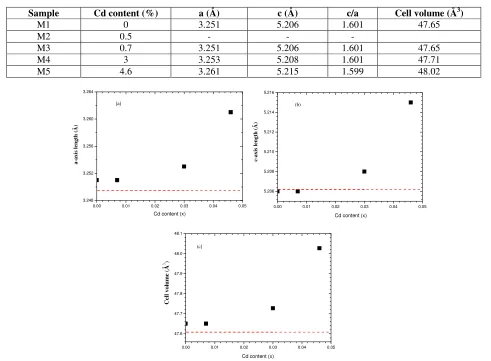
Table 2. Lattice parameters, c/a ratio and cell volume of Zn(1-x)Cdx0 solid solutions deposited on c-plane sapphire as function of cadmium content x.
Sample Cd content (%) a (Å) c (Å) c/a Cell volume (Å3)
M1 0 3.251 5.206 1.601 47.65
M2 0.5 - - -
M3 0.7 3.251 5.206 1.601 47.65
M4 3 3.253 5.208 1.601 47.71
M5 4.6 3.261 5.215 1.599 48.02
0.00 0.01 0.02 0.03 0.04 0.05 3.248
3.252 3.256 3.260 3.264
a-ax
is
le
ng
th
(Å
)
Cd content (x)
(a)
0.00 0.01 0.02 0.03 0.04 0.05 5.206
5.208 5.210 5.212 5.214 5.216
c-ax
is
le
ng
th
(Å
)
Cd content (x)
(b)
0.00 0.01 0.02 0.03 0.04 0.05 47.6
47.7 47.8 47.9 48.0 48.1
Cd content (x)
C
el
l v
ol
um
e
(
Å
3)
(c)
Fig. 4. Cadmium content x dependence of (a) a-axis lattice length, (b) c-axis lattice length and (c) the cell volume. In all cases the dashed line represents the corresponding parameters of bulk ZnO [15].
Compared to the bulk crystal values (a=3.2495 Å and c=5.2062 Å) [15], there is a slightlattice deformation, assuming that the layer
is partially relaxed. The a-, c-axis lengths determined by HRXRD and the cell volume are plotted as functions of Cd content in Figure 4 (a), (b) and (c) respectively. The experimental errors of lattice parameter for all layers are estimated to be 0.003Å. There is a significant change, compared to ZnO layer grown on c-plane sapphire, of a, c layers lattice parameters and the unit cell volume for
cadmium content higher than 0.7%. Since for Cd content below 0.7% the Zn(1-x)CdxO parameter layer mimics that of the ZnO layer.
By comparing a and c lattice parameters with those calculated by the evolution equation established by Makino et al. [14], we note that the in - of - plane lattice parameters are similar, however those out -of - plane are different.
At higher cadmium content, the cell volume varied 0.8% for the layer grown on sapphire substrate from that of bulk ZnO. For the film deposited on ZnO, this variation is half of the predicted value (1.6%) obtained by assuming that this difference is caused by the
difference in the cation radii of Cd2+ (0.95Å) and Zn2+ (0.74Å). The ratio (c/a) is between 1.601 and 1.599 for all layers deposited on
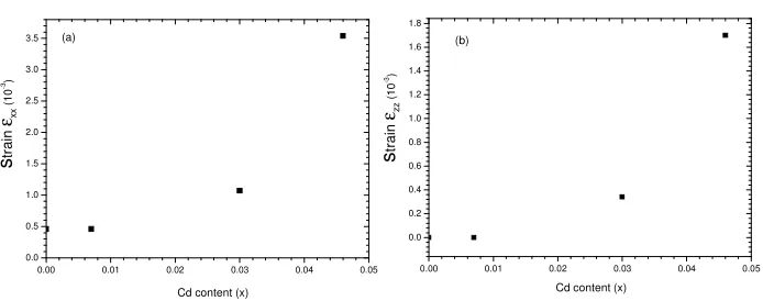
sapphire which differed very little from those of bulk ZnO (c/a=1.602). The in-plane (εxx) and out-plane (εzz) epitaxial strain is
0.00 0.01 0.02 0.03 0.04 0.05 0.0
0.5 1.0 1.5 2.0 2.5 3.0 3.5
Cd content (x)
s
tr
a
in
εxx
(
1
0
-3) (a)
0.00 0.01 0.02 0.03 0.04 0.05 0.0
0.2 0.4 0.6 0.8 1.0 1.2 1.4 1.6 1.8
(b)
Cd content (x)
s
tr
ain
εzz
(
1
0
-3)
Fig. 5. Epitaxial strain εxx (a) and εzz (b) of Zn(1-x)CdxO /c-plane sapphire as a function of cadmium content x.
The surface morphology of our film was observed by atomic force microscopy (AFM). All the AFM images were recorded with a
Nanoscape III a microscope from digital instruments Inc. in the tapping mode (25°C, in air). The film morphology of Zn(1-x)CdxO
grown on c-plane sapphire (scan area 5µm × 5µm ) are shown in Figure 6. The AFM images are shown in three and two dimensions
to see the difference in the morphology of layers as function of cadmium. The surface roughness of different samples was calculated from AFM images using the software “NanoRule” and the values obtained are presented in table 3.
ZnO/c-plane sapphire (x=0%)
Zn(1-x)CdxO/c-plane sapphire (x=0.7%)
Zn(1-x)CdxO/c-plane sapphire (x=3%)
Zn(1-x)CdxO/c-plane sapphire (x=4.6%)
Fig. 6. 3D (right) and 2D (left) AFM images of Zn(1-x)CdxO deposited on c-plane sapphire as function of Cd content.
Upon inspection of the images, ZnO deposited on c-plane sapphire the surface morphology consists of big and faceted grains with rms surface roughness of about 85nm. For solid solutions, the morphology surfaces appear rather rounded grain with a lower surface roughness. However, it is very difficult to correlate the change in surface roughness to that of cadmium content, especially since the film thicknesses are different. The change in grain shape is probably caused by the presence and relative orientations of the different areas of the charges resulted from the atomic arrangement but are disturbed by the incorporation of cadmium and the nature of the surface [16, 17].
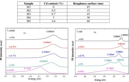
Sample Cd content (%) Roughness surface (nm)
M1 0 85
M2 0.5 15
M3 0.7 45
M4 3 30
M5 4.6 60
2.7 2.8 2.9 3.0 3.1 3.2 3.3 3.4
3.11eV
T=300K
Energy (eV)
P
l i
nte
ns
it
y
(a.
u)
x=0%
x=0.5%
x=0.7%
x=3%
x=4.6%
3.269eV
3.268eV
3.258eV
3.236eV
(a)
2.4 2.6 2.8 3.0 3.2 3.4
(b)
3.126eV 3.163eV
3.269eV3.356eV
Energy (eV)
P
l i
nt
en
si
ty
(
a.
u)
T=10K
x=0%
x=0.5%
x=0.7%
x=3%
x=4.6%
3.351eV
3.298eV
3.301eV
3.112eV
Fig. 7. Photoluminescence of different Zn(1-x)CdxO solid solutions grown on c-plane sapphire substrate (a) at 300K and (b) at 10K.
Photoluminescence (Pl) measurements were made for these different layers at room temperature using the 325 nm line of He-Cd
laser. Pl spectra at 10K and 300K of Zn(1-x)CdxO solid solutions grown on c-plane sapphire as function of cadmium content are
shown in Figure 7 (a) and (b). The observed Pl peak at room temperature of solid solutions shifts to lowers energies corresponding to the excitonic emission band when the cadmium content x increases. The full width at half maximum (FWHM) is about 130 meV for
x≤3% and about 150 meV for x=4.6%. The Pl spectra at low temperature show the disappearance of the typical fine structure of ZnO
[18-24] and the appearance of the shoulder at low energy which becomes more intense and wide as x increases. This is presumably due to larger compositional fluctuation and poorer crystallinity for larger x films. In fact, low temperature Pl spectroscopy is a suitable method to detect inhomogeneous potential fluctuation because the photo-excited carriers cannot travel long distance resulting in radiative recombination after relaxation into local potential minima. This same findings were reported by M. Kawasaki
[25] with Zn(1-x)CdxO films grown on sapphire (0001) substrates by pulsed laser deposition.
3 Conclusion
Zn(1-x)CdxO solid solutions have been grown on c-plane sapphire substrate by metal organic chemical vapor deposition with the
DMCd molar ratio range 0 to 10cc. The cadmium mole fraction was determined from energy band gap equation established by T. Makino [14]. Cd content has been seen to increase monotonically with the DMCd molar ratio until about x=4.6% which is significantly larger then thermodynamic solubility limit (2%). The XRD study revealed that all layers exhibit a wurtzite phase and
had a c-axis orientation. ω rocking curve measurement shows a poorer crystalline quality of layer. The microstructure of Zn(1-x)CdxO
layer grown on c-plane sapphire substrate compared to the reference sample M1, shows a significantmodification from x≥0.7%. The
Photoluminescence spectra show a gradual red shift indicating the narrowing of the band gap due to cadmium incorporation. Even
though, it is difficult to obtain high-crystalline quality Zn(1-x)CdxO films due to necessary low temperature growth, we can conclude
that this material is potential candidate for an active layer in blue LED based on ZnO.
Acknowledgements
References
1. A. Nakamura, J. Ishihara, S. Shigemori, K. Yamamoto, T. Aoki, H. Gotoh, J. Temmyo, Jpn. J. Appl. Phys. Part 2 44, L4 (2005)
2. J. J. Brown, F. A. Hummel, J. Electron. Soc. 111, 1056 (1964)
3. K. Agata, K. Maejima, Sz. Fujita, J. Cryst. Growth. 248, 25 (2003)
4. P. Fons, K. Iwata, S. Niki, A. Yamada, K. Matsubara, J. Cryst. Growth. 201/202, 627 (1999)
5. R. D. Vispute, V. Talyansky, Z. Trajanovic, S. Choopun, R. Downes, R. P. Sharma, T. Venkatesan, Appl. Phys. Lett. 70 (20),
2735 (1997)
6. E. S. Shim, H.S. Kang, J.S. Kang, J.H. Kim, S.Y. Lee, Appl. Surf. Sci. 186, 474 (2002)
7. V. Sallet, C. Thiandoume, J.F. Rommeluere, A. Lusson, A. Riviere, J.P. Riviere, O. Gorochov, R. Triboulet, V. Muñoz-Sanjosé,
Mater. Lett. 53, 126 (2002)
8. T. Gruber, C. Kirchner, K. Thonke, R. Sauer, A. Waag, Phys. Stat. Sol. A 192, 166 (2002)
9. S. H. Lim, D. Shindo, H.B. Kang, K. Nakamura, J. Cryst. Growth 225, 208 (2001)
10. A. Ohtomo, M. Kawasaki, Y. Sakurai, Y. Yoshida, H. Koinuma, P. Yu, Z.K. Tang, G.K.L. Wong, Y. Segawa, Mater. Sci. Eng.
B 54, 24 (1998)
11. F. Vigué, P. Vennéguès, S. Vézian, M. Laügt, J.P. Faurie, Appl. Phys. Lett. 79, 194 (2001)
12. D. F. Croxal, R. C. C. Ward, C. A. Wallace, R. C. Kell, J. Cryst Growth 22, 117 (1974)
13. J. Zûñiga-Pérez, V. Muñoz-Sanjosé, M. Loreng, G. Benndorf, S. Heitsch, D. Spemann, M. Grundmann, J. Appl. Phys. 99,
023514 (2006)
14. T. Makino, Y. Segawa, M. Kawasaki, A. Ohtomo, R. Shiroki, K. Tamura, T., Yasuda, H. Koinuma, Appl. Phys. Lett. 78, 1237
(2001)
15. F. Vigué, P. Vennéguès, C. Deparis, S. Vézian, M. Laügt, J. P. Faurié: J. Appl. Phys. 90, 5115 (2001)
16. J. Zûñiga-Pérez, V. Muñoz-Sanjosé, E. Palacio-Lidon, J. Colchero, Appl. Phys. Lett. 88, 261912 (2006)
17. J. Zûñiga-Pérez, E. Palacio-Lidon, V. Muñoz-Sanjosé, J. Colchero : Phys. Rev. Lett. 95, 226105 (2005)
18. D. C. Reynolds, C. W. Litton, T. C. Collins, Phys. Rev. 140, A1726 (1965).
19. Ü. Özgür, Ya. I. Alivov, C. Liu, A. Teke, M. A. Reshchikov, S. Doğan, V. Avrutin, S.-J. Cho, H. Morkoç, Appl. Phys. rev 98,
041301 (2005)
20. D. C. Reynolds, D. C. Look, B. Jogai, C. W. Litton, G. Cantwell, W. C. Harsch, Phys. Rev. B 60, 2340 (1999)
21. B. K. Meyer, H. Alves, D. M. Hofmann, W. Kriegseis, D. Forster, F. Bertram, J. Christen, A. Hoffmann, M. Strassburg, M.
Dworzak, U. Haboeck, A. V. Rodina, Phys. Stat. Sol. (b) 241, 231 (2004)
22. C. Gonzales, D. Block, R. T. Cox, A. Hervé, J. Cryst. Growth 59, 357 (1982)
23. A. Teke, Ü. Özgür, S. DOgan, X. Gu, H. Morkoç, B. Nemeth, J. Nause, H. O. Everitt, Phys. Rev. B 70, 195207 (2004)
24. B. K. Meyer, J. Sann, D. M. Hofmann, C. Neumann, A. Zeuner, Semicond. Sci. Technol. 20, S62 (2005)
25. M. Kawasaki, A. Ohtomo, R. Shiroki, I. Ohkubo, H. Kimura, G. Isoya, T. Yasuda, Y.Segawa, and H. Koinuma, Extended