Look-Up Tables on Reconfigurable Hardware
– Pitfalls of Memory Primitives –
Pascal Sasdrich1, Oliver Mischke1,2, Amir Moradi1, Tim G¨uneysu1
1 Horst G¨ortz Institute for IT-Security, Ruhr-Universit¨at Bochum, Germany
{pascal.sasdrich,oliver.mischke,amir.moradi,tim.gueneysu}@rub.de
2 Infineon Technologies AG, Chip Card & Security Division, Munich, Germany
Abstract. Block Memory Content Scrambling (BMS), presented at CHES 2011, enables an effective way of first-order side-channel protection for cryptographic primitives at the cost of a significant reconfiguration time for the mask update. In this work we analyze alternative ways to im-plement dynamic first-order masking of AES with randomized look-up tables that can reduce this mask look-update time. The memory prim-itives we consider in this work include three distributed RAM compo-nents (RAM32M, RAM64M, and RAM256X1S) and one BRAM primi-tive (RAMB8BWER). We provide a detailed study of the area and time overheads of each implementation technique with respect to the oper-ation (encryption) as well as reconfiguroper-ation (mask update) phase. We further compare the achieved security of each technique to prevent first-order side-channel leakages. Our evaluation is based on one of the most general forms of leakage assessment methodology known asnon-specific t-test. Practical SCA evaluations (using a Spartan-6 FPGA platform) demonstrate that solely the BRAM primitive but none of the distributed RAM elements can be used to realize an SCA-protected implementation.
1
Introduction
combinatorial masked circuits (for example see [8, 9]). Instead of masking com-binatorial circuits, critical elements such as S-boxes can be realized as look-up tables that are dynamically randomized in memory. A realization of such an approach on FPGAs which randomizes the content of block RAMs (BRAM) has been presented in [4] and is known as Block Memory Content Scrambling (BMS).
Contribution: In this work we analyze the suitability of different Xilinx FPGA memory primitives to prevent first-order side-channel leakage by masked look-up tables. Besides using larger dual-port BRAM primitives (as used in the original BMS publication [4]), it is also possible to use smaller single-port BRAMs as well as distributed RAM elements which are realized in SLICE-M LUTs of modern Xilinx FPGAs [12]. With the introduction of Xilinx’ Virtex-5 platform SLICE-M have become capable to hold 256 bits of memory that is a perfect fit for an 8×256-bit AES S-box. In particular RAM32M, RAM64M, and RAM256X1S are the primitives which can be used to build a randomly permuted (masked) S-box. Although reconfiguration time becomes notably shorter for smaller RAM module sizes, the total area requirements of each masked S-box increases.
For evaluation we apply the non-specifict-test as a general leakage assessment methodology [3] to analyze the SCA resistance of each scheme. We show that due to their intrinsic multi-LUT design, the distributed RAM elements still exhibit a first-order leakage so that they should not be used to implement masked designs. We conclude our work with presenting an efficient implementation of a small single-port BRAM-based design that achieves almost double the throughput of the original BMS scheme and still prevents first-order leakages.
Outline: This work is organized as follows: Section 2 introduces the underlying FPGA primitives, explains how they can be employed to realize randomized look-up tables and recalls the BMS scheme. In Section 3 our masked AES encryption designs are presented and their reconfiguration time, resource requirements, and throughput are compared. Practical evaluation of all implementation profiles is given in Section 4, before we conclude our work in Section 5.
2
Preliminaries
In this section we briefly describe memory primitives provided by Xilinx FPGAs and their application in order to build randomized look-up tables to protect cipher implementations against first-order DPA attacks. Afterwards, we restate the concept of Block Memory Content Scrambling (BMS) initially introduced in [4].
2.1 Memory Primitives
randomly permuted look-up tables. Distributed memories are enabled only at special Slices (SLICE-M) by using the configuration registers within the Look-Up Tables (LUTs) as general purpose memory cells. Since this memory is usually constrained by the configuration size (between 16 and 64 bits), up to 4 LUTs of a single SLICE-M can be combined in order to build larger RAMs. For de-signs requiring even larger amounts of memory, FPGAs provide general purpose block memory (BRAM) with memory sizes between 8 Kbits and 32 Kbits. In the following we describe these memory primitives and their modes of operation in detail, focusing on their application as a randomized look-up table (see [12] for more information).
RAM32M The RAM32M memory primitive is a multi-port random access memory with synchronous write but asynchronous read capability imple-mented in distributed memory using the configuration memory of all LUTs (and both outputs O6 and O5) of a single SLICE-M. It is organized as an 8-bit wide by 32 deep memory providing 4 individual read ports (each 2-bit wide) and a single write port (8-bit wide). If all read addresses are tied to the same value, this memory primitive becomes an 8×32 single port RAM. RAM64M In contrast to the RAM32M primitive, the RAM64M module is a multi-port random access memory with synchronous write and asynchronous read capability organized as 4-bit by 64 deep memory. This memory primitive also occupies 4 LUTs of a SLICE-M but only uses the outputs O6 of the LUTs. If all 6-bit wide address ports are tied to the same value, this memory becomes a 4×64 single port RAM.
RAM256X1S Another option for distributed memory is RAM256X1S. This primitive is a single-port random access memory with synchronous write and asynchronous read capability placed in a single SLICE-M using all LUTs (combined by subsequent MUXF7 and MUXF8 multiplexer instances). A RAM256X1S provides an 8-bit wide address port and a 1-bit wide read and write port and is organized as a 1×256 single port RAM.
RAMB8BWER The RAMB8BWER primitive is a true dual-port random ac-cess memory with synchronous read and write capability. Instead of using configuration memory of special LUTs as distributed memory, this RAM in-stance occupies a dedicated block memory primitive and offers 8 Kbits data storage in addition to a 1 Kbit parity memory. It is possible to define differ-ent options and widths for the read and write ports changing the memory configuration from 1×8 Kbits up to 9×1 Kbit. The embedded input register causes this primitive to always require a clock cycle to read from an address (synchronous). In addition, the output port can use an additional embedded register in order to buffer the memory output leading to two clock cycles latency for a read operation.
2.2 Randomized Look-Up Tables
S-boxes can efficiently be realized either using LUTs (as well as distributed memories) or block memories depending on their size as well as the available resources.
SCA attacks target an intermediate value of a cipher, e.g., a part of the non-linear layer. The predicted intermediate values, usually the input or output of a known S-box, in addition to a hypothetical power model contribute in a statistical analysis of e.g., power consumption traces in order to reveal the asso-ciated secret. In order to avoid side-channel leakages, hardware designers need to apply dedicated countermeasures e.g., masking. These countermeasures aim at randomizing intermediate values of a cipher implementation using uniformly-distributed random data (masks). In particular, the non-linear layer in terms of look-up tables such as S-boxes (or T-Tables) has to be adapted depending on the taken random mask. Usually this is done by scrambling the S-box content based on an input maskmand adding an output masknto the content (Boolean masking), so that the masked S-boxS0 is precomputed as:
S0(x⊕m) =S(x)⊕n
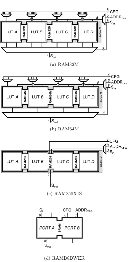
As mentioned before, look-up table based S-boxes can be implemented using distributed or block memories. Due to their reconfiguration feature, the above-presented memory primitives can be employed to implement randomized look-up tables as well. Figure 1 exemplarily shows a part of the structure of an AES S-box using RAM32M (Figure 1a), RAM64M (Figure 1b), RAM256X1S (Figure 1c) and RAMB8BWER (Figure 1d) memory primitives.
Each of the distributed memory designs presented in Figure 1 realizes one bit of the AES S-box. Each of them receives an 8-bit input Sin, and provides
one output bitSout. Depending on their read/write port width the configuration
to update the look-up table is defined. For example, the content of 8 bits of a RAM32M can be updated in one clock cycle (Figure 1a) while at most 4 bits of RAM64M and 1 bit of RAM256X1S can be simultaneously updated. This clearly affects the efficiency of the update (reconfiguration) process. Respectively, ex-tra components, i.e., the multiplexers in Figure 1, have to be placed out of the SLICE-M to build a 1×256 memory. With respect to this issue RAM256X1S is the most efficient one while the time required to update its content is consider-ably higher than the other distributed memory primitives.
2.3 Block Memory Content Scrambling
LUT A LUT B LUT C LUT D Sout RAM32 M RAM32 M RAM32 M ADDRCFG Sin CFG 8 5 8 3 5 1 SLICE-M (a) RAM32M SLICE-M
LUT A LUT B LUT C LUT D
Sout RAM64 M RAM64 M RAM64 M ADDRCFG Sin CFG 4 6 8 2 6 1 (b) RAM64M SLICE-M
LUT A LUT B LUT C LUT D
Sout RAM25 6 RAM25 6 RAM25 6 ADDRCFG Sin CFG 1 8 8 1 (c) RAM256X1S BRAM ADDRCFG CFG Sin Sout
PORT A PORT B
8
8 8 8
(d) RAMB8BWER
the encryption process while the active context becomes passive and is updated using a new (random) mask. This scrambling scheme exploits the true dual-port capability of BRAM in order to randomize look-up tables such as S-boxes or T-Tables without affecting the throughput of the encryption scheme. Despite many advantages, this scheme comes with
– area overhead, since it doubles the memory requirements because every look-up table has to be stored twice (active and passive), and
– additional latency for a mask update process, as the scrambling (updating) process needs 512 clock cycles. Hence it often happens that the consecutive encryptions share the masks since the scrambling process is not finished when the second plaintext is given.
3
Design
This section briefly explains the underlying masking scheme of our AES imple-mentation and its basic hardware architecture. Afterwards, different approaches using the distributed memory and the block memory primitives are compared.
3.1 Masking Architecture
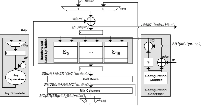
The architecture of our design of the AES-128 encryption function (for a Spartan-6 FPGA) is shown in Figure 2. We opted to implement an incremental and round-based architecture and derive the round keys on the fly. The data path has a width of 128 bits, and the SubBytes layer consists of 16 parallel reconfigurable S-boxes. ShiftRows and MixColumns (in parallel on all 4 columns) are applied jointly at one clock cycle.
In contrast to the originally proposed BMS scheme, our design follows an approach based on an update-prior-to-encryption fashion. Thus, before each en-cryption the randomized look-up tables are regenerated. During each enen-cryption the masks stay constant. In other words, the same masks are used for all cipher rounds during one encryption. The initial plaintext is masked with (m⊕m0) while all round keys are masked withm0 (m andm0 independent of each other and each 128-bit). Therefore, after the key addition the SubBytes input mask is
m(see Figure 2). The randomized look-up tables (masked SubBytes) are config-ured withmas the input mask andSR−1(M C−1(m⊕m0)) as the output mask.
Applying the ShiftRows and MixColumns operations transforms the mask again to (m+m0) as the mask of the round output. Hence, after each cipher round the input to the next round is masked with (m⊕m0) and no mask correction (see [2] and [10]) is required. For the last round, the MixColumns operation is omitted and the returned ciphertext is masked with M C−1(m⊕m0)⊕m0.
Randomized
Look-UpKTables
Configuration Generator
... S15
MixKColumns ShiftKRows p⊕m⊕m'
c⊕MC-1(m⊕m')⊕m'
Configuration Counter
addr cfg
S
SR-1(MC-1(m⊕m'))
m
S0
KeyKSchedule Key Expansion
0 1
m' Key
k⊕m'
0 1 SB(p⊕k)⊕SR-1(MC-1(m⊕m'))
SR(SB(p⊕k))⊕MC-1(m⊕m')
MC(SR(SB(p⊕k)))⊕(m⊕m') (p⊕k⊕m)
0 1
last first
first
Fig. 2: Round-based AES implementation with randomized look-up tables
(HD) model, is easily extractable. If x⊕mand y⊕mare consecutively stored in a register,
HD(x⊕m, y⊕m) =HW(x⊕y)
is independent of the mask. Hence, we avoid such an issue by surrounding each S-box with two register stages, one before and one after the SubBytes operation (see Figure 2). At power-up both registers are precharged with 0, and at only one clock cycle the input multiplexer passes the masked plaintext (p⊕m⊕m0). Since one of the register stages therefore holds some value depending on a random mask of a previous encryption, the correct encryption rounds are interleaved with random (dummy) operations.
Employing this technique leads to reduced throughput due to the prior look-up table look-update phase as well as the fact that each cipher round requires two clock cycles. However, compared to BMS [4] our design reduces the area overhead as well as the amount of required randomness to 256-bit per encryption (mand
m0). Further, this scheme is suitable for the distributed memory primitives as well as for the block memory which allows a fair comparison. In case the block memory is used, the registers (before and after the SubBytes) are removed. Instead, the input and output registers of the block memory are employed as the two-stage state registers.
3.2 Comparison of S-box designs
Table 1: Comparison of S-boxes for different memory primitives
Memory SubBytes Configuration
Primitive Logic Dist. Mem. Block Mem. Logic Memory
(LUT) (LUT) (BRAM16) (LUT) (FF)
BRAM (BMS) none none 16 1706* 1169*
RAMB8BWER none none 8 298 8
RAM256X1S 128 512 none 298 8
RAM64M 768 512 none 727 6
RAM32M 1920 512 none 1222 5
* These values are based on a Virtex-II Pro implementation and taken from [4]. For a Spartan-6 the resulting design would be slightly smaller.
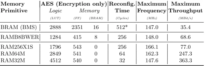
Table 2: Time and resource requirements of entire AES (encryption only)
Memory AES (Encryption only) Reconfig. Maximum Maximum
Primitive Logic Memory Time Frequency Throughput
(LUT) (FF) (BRAM) (Cycles) (MHz) (MBit/s)
BRAM (BMS) 2888 2351 16 512* 147.0 35.4
RAMB8BWER 1284 415 8 256 148.0 68.6
RAM256X1S 1796 543 0 256 166.1 77.0
RAM64M 2849 541 0 64 162.3 247.3
RAM32M 4512 540 0 32 147.6 363.3
* Reconfiguration can be done in parallel when reusing the mask for multiple encryptions without affecting the throughput. For a fair comparison we avoid the mask reuse in BMS as well.
and throughput. Compared to the originally proposed BMS scheme, our masked design based on the block memory (RAMB8BWER) halves the reconfiguration time, hence nearly doubling the maximum throughput. In case the distributed memory primitives are employed, the maximum frequency can even be increased except for the RAM32M due to its more complex reconfiguration circuit. Besides, the RAM32M leads to the highest throughput as its reconfiguration time is ex-tremely shorter than the others. Note that in the reported performance figures we omitted the area required for the generation of the random masks.
4
Evaluation
We employed a SAKURA-G platform [5], i.e., a Spartan-6 FPGA, for practical side-channel evaluations. The power consumption traces have been measured by means of a LeCroy WaveRunner HRO 66Zi oscilloscope with a 1 Ω resistor in the Vdd path capturing the embedded amplifier output of the SAKURA-G.
4.1 Non-Specific Statistical t-test
In order to examine the resistance of our designs we applied the leakage assess-ment methodology (t-test) of [3]. The most general form of such a test – known
as non-specific t-test – investigates the existence of a first-order leakage
inde-pendent of any power model as well as any intermediate value. In such a test a certain plaintext is selected, and during the measurements the chosen plaintext or a random one is given to the encryption module in a randomly-interleaved fashion. For all the measurements the key is kept constant. Therefore, this test is also calledfix vs. random t-test. As the next step the traces are categorized into two groupsG1 andG2based on their associated (fix or random) plaintext. By comparing the means of these groups, we can examine the dependency of the traces (leakages) to the processed values related to the given plaintexts. Such a comparison can be fairly performed by means of a Welch’s (two-tailed)t-test as
t= µq(T ∈G1)−µ(T ∈G2)
δ2(T∈G 1)
|G1| + δ2(T∈G
2)
|G2|
,
where µ andδ2 denote the sample mean and the sample variance respectively, and|.|the cardinality.
As the final step the obtainedtwith the correspondingdegree of freedom3is given to the cumulative Student’s tdistribution function to achieve a quantita-tive value as the probability of thenull hypothesisbeing valid. Such a hypothesis is the assumption that the samples in the groupsG1andG2were drawn from the same population, i.e., the two groups are not distinguishable. However, for sim-plicity a threshold for thet-test result as|t| > 4.5 is usually selected to reject the null hypothesis and conclude that the means of the groups are distinguishable, hence there exists a leakage.
It is noteworthy that the scenario explained above should be repeated at each sample point of the power traces independently, hence a first-order univariate evaluation. On one hand, when the result of a test is positive, the value of the
t statistic gives the level of confidence that there exist a first-order leakage, but it does not provide any information about the difficulty or easiness of an attack exploiting such a leakage. On the other hand, in case a non-specifict-test reports no leakage, such a conclusion is only correct with respect to the selected fix plaintext as well as the number of used traces. Changing the fix plaintext and increasing the number of traces can change the result of the test. The same evaluation scheme has also been applied in [1].
4.2 Results
In the following we present the results of the security evaluation concerning side-channel resistance of randomized look-up tables using the introduced memory primitives by applying the above-explained non-specifict-test. Since we identified
3
1 3 5 7 0
30
Time [µs]
Voltage [mV]
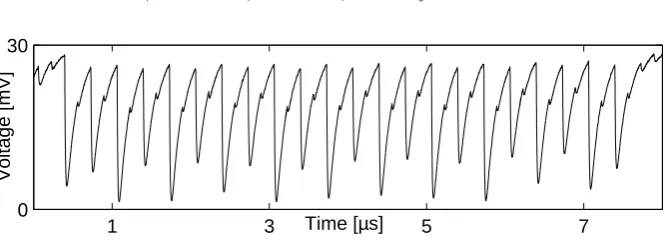
Fig. 3: Sample trace
four potential memory elements (see Section 2.1), the evaluations are grouped into four different profiles respectively.
A sample trace of the profile built from RAM64M modules is shown in Fig-ure 3. Note that all our measFig-urements cover only the time period related to the encryption, and we ignored to measure the power consumption when the reconfiguration of the look-up tables is in process (prior to each encryption). As explained in Section 3, we kept the design architecture of all profiles the same. Hence the power traces of other profiles look like the same, but for the design profile with RAM32M the traces show slightly higher peak-to-peak amplitude due to its more complex architecture regarding the extra multiplexers out of the RAM slices.
For each profile we collected at least 1 million traces for a non-specifict-test. During all the measurements fresh masks are randomly generated by means of an AES engine running in counter mode prior to each encryption, i.e., no mask is reused. The masked plaintext in addition to the corresponding masks are sent from the control FPGA to the target FPGA (SAKURA-G). After finishing the look-up table reconfiguration followed by the encryption process on the target FPGA, the masked ciphertext is sent back to the control FPGA, where it is unmasked for a consistency check.
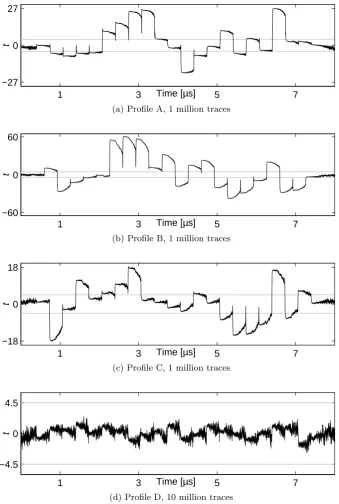
Profile A: Tiny RAM (RAM32M) By means of this profile we evaluate the leakage of the randomized look-up table realized by RAM32M memory primi-tives. Although this variant has the highest resource consumption, it offers the best throughput. Figure 4a shows the result of the corresponding non-specific
t-test using 1 million traces (i.e., about 500 000 traces of encrypting the fix plain-text and the rest for the random ones). Unexpectedly the test exhibits first-order leakages. Indeed, the tstatistics are much higher than the threshold, that con-fidently argue the vulnerability of the design.
1 3 5 7 −27
0 27
Time [µs]
t
(a) Profile A, 1 million traces
1 3 5 7
−60 0 60
Time [µs]
t
(b) Profile B, 1 million traces
1 3 5 7
−18 0 18
Time [µs]
t
(c) Profile C, 1 million traces
1 3 5 7
−4.5 0 4.5
Time [µs]
t
(d) Profile D, 10 million traces
unexpected first-order leakages. Interestingly, the amount of leakage is higher compared to that of Profile A, although its S-box design is more compact.
Profile C: Large RAM (RAM256X1S) The most compact and dense imple-mentation for a randomized look-up table using Distributed Memory (i.e., the RAM256X1S memory primitives) on a Spartan-6 FPGA, places the a complete single AES S-box and the subsequent registers into only 8 slices. However, the same as the two former design profiles a first-order leakage is still detectable which can be seen in Figure 4c.
Profile D: Block RAM (RAMB8BWER) As the last profile we evaluated the application of block RAMs instead of the Distributed Memory. Since each block RAM internally has a register stage for the input and an optional one for the output, by employing a RAMB8BWER instance for each S-box we used also both internal registers of the block RAM and avoided the external registers used in the other profiles (see Figure 2). Since we did not observe any first-order leakage using the same number of traces as used for the other profiles, we performed the evaluation using 10 million traces. The corresponding result is shown in Figure 4d indicating the ability of the design to prevent any first-order leakage.
In fact, the results we presented above infer the pitfall of using distributed memories (of FPGAs) to realize randomized (masked) look-up tables. While the internal architecture of such memory primitives is not completely clear to us, we are confident that the observed leakage is due to the internal multiplexers of such memory modules. We should highlight that the randomized look-up tables (in our designs) receive only the masked inputs and provide the masked outputs. Neither the input mask nor the output mask is given to the memory module. Further, the input masks and output masks are independent of each other. As a result – also confirmed by the evaluation result of Profile D – the exhibited leakage is purely related to the internal architecture of the distributed memory modules.
5
Conclusion
Our design solution using block memory (RAMB8BWER) achieves almost double the throughput compared to the original BMS mainly because of the reduced reconfiguration time of the masked S-boxes. It also requires less ran-domness. The BMS scheme is a T-table implementation which requires 16×32 random bits to mask the T-tables output while we only require 2×128 bits of randomness. The reason for this difference is that we are only implementing the 8×8 AES S-box as masked tables (compared to 8×32 T-tables) while the other parts (all linear) of the encryption are implemented by combinatorial logic.
References
1. B. Bilgin, B. Gierlichs, S. Nikova, V. Nikov, and V. Rijmen. Higher-Order Thresh-old Implementations. InASIACRYPT 2014, volume 8874 ofLNCS, pages 326–343. Springer, 2014.
2. J. Bringer, H. Chabanne, and T. Le. Protecting AES against side-channel analysis using wire-tap codes. J. Cryptographic Engineering, 2(2):129–141, 2012.
3. G. Goodwill, B. Jun, J. Jaffe, and P. Rohatgi. A testing methodology for side-channel resistance validation. In NIST Non-Invasive Attack Testing Workshop, Nara, 2011.
4. T. G¨uneysu and A. Moradi. Generic Side-Channel Countermeasures for Recon-figurable Devices. In B. Preneel and T. Takagi, editors, Cryptographic Hardware and Embedded Systems - CHES 2011, Nara, Japan, September 28 - October 1, 2011. Proceedings, volume 6917 ofLecture Notes in Computer Science, pages 33– 48. Springer, 2011.
5. H. Guntur, J. Ishii, and A. Satoh. Side-channel AttacK User Reference Architecture SAKURA-G. InGCCE 2014. IEEE Computer Society, 2014. Further information are available viahttp://satoh.cs.uec.ac.jp/SAKURA/index.html.
6. P. C. Kocher, J. Jaffe, and B. Jun. Differential Power Analysis. In M. J. Wiener, editor, Advances in Cryptology - CRYPTO ’99, Santa Barbara, California, USA, August 15-19, 1999, Proceedings, volume 1666 ofLecture Notes in Computer Sci-ence, pages 388–397. Springer, 1999.
7. S. Mangard, E. Oswald, and T. Popp.Power analysis attacks - revealing the secrets of smart cards. Springer, 2007.
8. S. Mangard, N. Pramstaller, and E. Oswald. Successfully Attacking Masked AES Hardware Implementations. In J. R. Rao and B. Sunar, editors, Cryptographic Hardware and Embedded Systems CHES 2005, Edinburgh, UK, August 29 -September 1, 2005, Proceedings, volume 3659 of Lecture Notes in Computer Sci-ence, pages 157–171. Springer, 2005.
9. A. Moradi, O. Mischke, and T. Eisenbarth. Correlation-Enhanced Power Analysis Collision Attack. In S. Mangard and F. Standaert, editors,Cryptographic Hardware and Embedded Systems, CHES 2010, Santa Barbara, CA, USA, August 17-20, 2010. Proceedings, volume 6225 ofLecture Notes in Computer Science, pages 125– 139. Springer, 2010.
10. M. Nassar, Y. Souissi, S. Guilley, and J. Danger. RSM: A small and fast coun-termeasure for AES, secure against 1st and 2nd-order zero-offset SCAs. InDATE 2012, pages 1173–1178. IEEE, 2012.
in Europe Conference and Exposition (DATE 2004), 16-20 February 2004, Paris, France, pages 246–251. IEEE Computer Society, 2004.