Abstract
Morgan, Andrew Stacy. Design Flow Based on Sensitivity Analysis For High-speed Digital Circuits. (Under the guidance of Dr. Paul D. Franzon)
Biography
Acknowledgements
I wish to express my appreciation to my advisor Dr. Paul Franzon for his continuous support, guidance, and inspiration through the course of this project and through the course of my graduate study as a whole. It has been an honor and pleasure to work with and learn from him.
I would also like to thank Dr. Griff Bilbro and Dr. W. Rhett Davis for serving on my committee and also providing guidance throughout my undergraduate and graduate studies. It has been a pleasure working with Dr. Bilbro as a teaching assistant to strengthen undergraduate analog electronics and inspire young circuit designers. I would also like to recognize the valuable experience I gained while working with Dr. Davis early in my Master’s program, and express my appreciation for his influence through my coursework and individual study.
Special thanks goes to my mother and father for their unconditional love and support throughout the duration of my college career. Thanks, particularly to my mother, for her gentle encouragement to pursue a graduate degree, even when my impatience began to get the better of me. Both of my parents contributed different, yet very valuable positive influence on my personality that helped to mold the man and engineer that I am proud to have become.
A very special thanks goes to my fiancé, Jayne, whose patience, understanding, and unconditional love and encouragement fueled the accomplishments of my graduate career at NCSU. My success would be hollow without her love and support.
Table of Contents
Page
List of Tables ...vii
List of Figures ...viii
1. Introduction...1
2. Background and Motivation ...1
3. General Design Flow ...3
3.1.Design Goals...3
3.2.Hand Analysis...3
3.3.Parametric Analysis ...3
3.4.Analysis of Parasitics...6
3.5.Software Utilization...8
3.6.Simulation Utilization...9
3.7.Interpreting Results...10
4. Source Follower Design Example ...11
4.1.Description...11
4.2.Common Applications ...12
4.3.Specific Application ...12
4.4.Advantages of Topology...13
4.5.Disadvantages of Topology ...13
4.6.Design Approach ...13
4.7.Analysis Setup and Approach...16
4.9.Key Considerations...22
5. Gate-Isolated Voltage Sense-Amplifier Design Example ...26
5.1.Description...26
5.2.Specific Application ...28
5.3.Advantages of Topology...28
5.4.Disadvantages of Topology ...29
5.5.Design Approach ...29
5.6.Analysis Setup and Approach...31
5.7.Sensitivity Analysis ...31
5.8.Key Considerations...43
6. Schmidt Trigger Design Example...47
6.1.Description...47
6.2.Specific Application ...48
6.3.Advantages of Topology...48
6.4.Disadvantages of Topology ...49
6.5.Design Approach ...49
6.6.Analysis Setup and Approach...53
6.7.Sensitivity Analysis ...53
6.8.Key Considerations...60
7. Dual-rail Domino Logic Design Example ...63
7.1.Description...63
7.2.Specific Application ...65
7.4.Disadvantages of Topology ...66
7.5.Design Approach ...66
7.6.Analysis Setup and Approach...68
7.7.Sensitivity Analysis ...69
7.8.Key Considerations...78
8. Conclusions and Future Work ...80
8.1.Insight into the Design Flow...80
8.2.Future Work ...80
9. References...82
10.Appendix A...83
• Id Curves for TSMC 0.18um Process Generated using Hspice...83
• Id Curves for TSMC 0.18um Process Generated using Matlab...86
• Matlab Script for Generating Id Curves...88
• Matlab Script for Calculating Wopt...90
List of Tables
Page
3.1 NMOS Parasitic Capacitance Calculations...7
3.2 PMOS Parasitic Capacitance Calculations ...8
4.1 Sensitivity Results for Scaling M0 ...19
4.2 Sensitivity Results for Scaling M1 ...21
4.3 Sensitivity Results for Scaling M0 & M1...22
5.1 Nominal Gate Widths for Sense-Amplifier ...31
5.2 Sensitivity Results for Scaling N6 ...32
5.3 Sensitivity Results for Scaling N1-N4...34
5.4 Sensitivity Results for Scaling N1-N4 & N6...37
5.5 Sensitivity Results for Scaling P1 & P4 ...37
5.6 Delay Sensitivity to Common-mode Input Voltage Shift...40
5.7 Delay Sensitivity to Allowed Aperture Time ...42
6.1 Nominal Gate Widths for Schmidt Trigger ...52
6.2 Sensitivity Results for Scaling NF & PF ...55
6.3 Sensitivity Results for Scaling N1 & P1...56
6.4 Sensitivity Results for Scaling NF, PF, N1, & P1 ...57
6.5 Sensitivity Results for Scaling N2 & P2...60
7.1 Nominal Gate Widths for Dual-rail Domino AND Gate ...67
7.2 Sensitivity Results for Scaling Mp1 & Mp2...71
7.3 Sensitivity Results for Scaling Mf1 & Mf2 ...72
7.4 Sensitivity Results for Scaling M0-M3 & Me ...74
7.5 Sensitivity Results for Altering Progressive Sizing...77
7.6 Sensitivity Results for Scaling Me...79
List of Figures
Page
3.1 Id Curves for NMOS with W/L=270nm/180nm in 0.18um (Deep) Process ...4
3.2 Parametric Analysis Test Circuit ...5
4.1 Source Follower Schematic w/ Nominal Sizes...11
4.2 Minimum Eye Width Sensitivity Comparison...17
4.3 Vout,CM Sensitivity Comparison ...18
4.4 Eye Diagram for W1 Scaled Down by 50% ...20
4.5 Eye Diagram for W1 Scaled Up by 100% ...20
4.6 Average Power Comparison ...23
4.7 Minimum Eye Height Sensitivity Comparison...25
5.1 Sense-Amplifier Schematic w/ Nominal Sizes ...27
5.2 Sensitivity Results for Scaling N6 ...33
5.3 Sensitivity Results for Scaling N1-N4...35
5.4 Sensitivity Results for Scaling N1-N4 & N6...38
5.5 Sensitivity Results for Scaling P1 & P4 ...39
5.6 Pre-charge Sensitivity Comparison...40
5.7 Delay Sensitivity to Common-mode Input Voltage Shift...41
5.7a Single-Ended Transient Response Plots Common-mode Shifting ...41
5.8 Delay Sensitivity to Allowed Aperture Time ...42
5.8a Single-Ended Transient Response Plots for Aperture Time Sweep ...43
5.9 Clock-to-Output Sensitivity Comparison ...44
5.10 Average Power Comparison ...44
5.11 Power-Delay Product Sensitivity Comparison ...45
6.1 Schmidt Trigger Schematic w/ Nominal Sizes ...47
6.2 Sensitivity of VIH and VIL to Scaling P1, PF, N1, and NF...54
6.3 Propagation Delay (TP) Sensitivity Comparison ...58
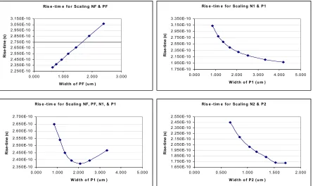
6.4 Rise Time Sensitivity Comparison ...59
6.5 Fall Time Sensitivity Comparison ...59
6.6 Average Power Comparison ...61
6.7 Propagation Delay High-to-Low (TPHL) Sensitivity Comparison...62
6.8 Propagation Delay Low-to-High (TPLH) Sensitivity Comparison...62
7.1 Dual-rail Domino AND Gate Schematic w/ Nominal Sizes...64
7.2 Pre-charge Rise-time on Node ‘c’ Sensitivity Comparison...70
7.3 Pre-charge Rise-time on Node ‘cbar’ Sensitivity Comparison...70
7.4 Worst-case Propagation Delay (for inputs AB=01) Sensitivity Comparison ...75
7.5 Power-Delay Product Sensitivity Comparison ...75
7.6 Pre-charge Propagation Delay on Node ‘c’ Sensitivity Comparison...76
A.1 Id Curves for NMOS with W/L=2.7um/180nm in 0.18um (Deep) Process ...83
A.2 Id Curves for NMOS with W/L=27um/180nm in 0.18um (Deep) Process ...84
A.3 Id Curves for NMOS with W/L=270um/180nm in 0.18um (Deep) Process ...85
A.4 Id Curves for NMOS with W/L=270nm/180nm Generated in Matlab...86
A.5 Id Curves for NMOS with W/L=2.7um/180nm Generated in Matlab...86
A.6 Id Curves for NMOS with W/L=27um/180nm Generated in Matlab...87
1. Introduction
The focus of this thesis is to develop a design flow for high-speed digital circuits that share common design characteristics. The design flow will include an analysis of the sensitivity of overall performance to changes in various circuit parameters and identify design “pressure points”. The ultimate goal is to produce a collection of design examples that can be used as an instructional tool for students taking ECE733 – Digital Electronics at NC State University. The examples should document the thought process for circuit optimization and provide a finished product that can be used as a reference point for similar designs. The intent is that students can derive a better understanding of how the circuit works and hopefully develop a general approach to design that can be applied to other problems. The approach to be presented will utilize analysis and design techniques presented in lecture and textbooks, as well as convenient simulation techniques that take advantage of the power of SPICE. The performance data collected during the analysis is presented in both tabular and graphic form to best illustrate the circuits’ sensitivity due to scaling the values of select variables.
2. Background and Motivation
decreases. To reduce the complexity of the math, approximations and assumptions must be made to eliminate variables, further reducing the accuracy of the results from hand analysis.
Because these techniques demonstrate the concepts that govern circuit operation, circuits must be taught using hand analysis. One can understand how a circuit works and get a sense of what parameters are significant by examining the generic topology and governing equations. The approximations, assumptions, and “ignoring for now” reductions must be made to understand the “big picture.” However, the neat and clean results that hand analysis yields describing circuit behavior can give the designer a false sense of the expected performance of his circuit. This is not to imply that hand analysis and design should not be practiced, but suggest that the presentation of such analyses be supplemented by practical application.
3. General Design Flow
Given the preceding discussion, a combination of hand and simulation analyses seems
to provide the most thorough presentation of circuit design. Therefore I propose to
structure the design flow as follows:
3.1.Design Goals: When first approaching a design problem, the goals for circuit
performance must be clearly understood before it can be optimized. Once the most
important and/or challenging design specifications are identified, a topology that
most nearly meets the desired performance may be analyzed and chosen. Without a
clear design goal, the tradeoffs among performance parameters may appear endless.
3.2.Hand Analysis: After a topology has been chosen, every design must still begin with
some sort of hand analysis to approximate the values for independent variables that
the designer can control, such as device dimensions, passive component values, bias
voltages or currents, etc. This initial analysis of the circuit will characterize its
general operation and identify which parameters are most significant. The equations
derived for the circuit will allow the designer to develop “rules of thumb” for
adjusting variables within the circuit to move towards the desired output.
3.3.Parametric Analysis: Once the designer has an intuitive understanding of how the
circuit is supposed to work, he must analyze the accuracy of his equations versus
models that will be used in simulation. For example, this comparison requires
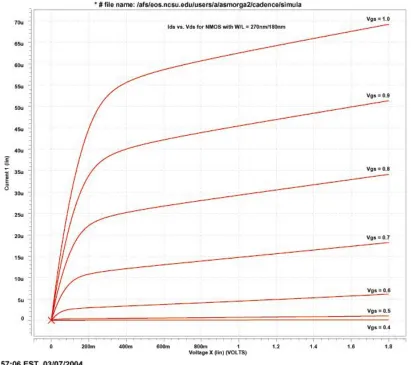
parametric analysis for the transistors in the process the designer plans to use. The
designer should produce his own Id curves over ranges of Vds and Vgs to create a
reference during design, as was done in Figure 3.1. This analysis will give the
Figure 3.1 - Id Curves for NMOS with W/L=270nm/180nm in 0.18um (Deep) Process
he designs on paper and what he sees in simulation. Realizing these differences is
very important when considering current drive capability, output impedance,
threshold voltage, and biasing conditions. The curves in Figure 3.1 were produced
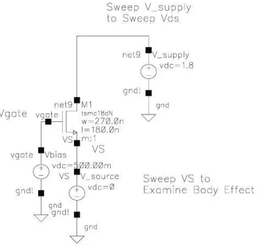
using the circuit in Figure 3.2 and simulated using Hspice. Similar plots, shown in
Figures A.1-A.3 of Appendix A, were created using scaled transistor widths of
2.7um, 27um, and 270um to examine how closely the drain current scales with width.
Figure 3.2 - Parametric Analysis Test Circuit
were compared to Matlab simulation results. Using the unified model equations for
drain current and beginning with process parameters1 taken from the TSMC 0.18um
(Deep) model file, the parameters were adjusted until the Matlab Id vs. Vds curves
closely matched those of the Hspice results.2 This adjusted set of process parameters
was used for the examples presented in the later sections. In those examples, the
transistors are assumed saturated and the drain current is modeled using the first order
approximation in Eqn. 3.1, where V V
V uA
Cox ton
n =100 2, =0.43
µ . 3
1 “process parameters” refers to the process transconductance parameter (µC
ox), the threshold voltage (Vth), and
the saturation drain voltage (Vdsat).
(
)
2 21 n ox gs t
d V V
L W C
I = µ − Eqn. 3.1
Keeping modeling error in mind, the designer can estimate the rough sizes of
transistors and begin the design in the right ballpark. General biasing conditions can
also be determined from hand analysis. Then, using Hspice DC analysis, one can
determine a more exact DC operating range and the preferred bias condition for the
application. Analyzing the voltages, currents, and capacitances at critical nodes for
extreme values of the transient range and during transients will reveal effects that
were not included in the hand calculations and must be accounted for.
3.4.Analysis of Parasitics: The parasitic capacitors within devices will add internal loads
that must be accounted for during optimization. For the purposes of hand analysis,
first order approximations for gate and bulk capacitances give reasonable results for
the expected impact on load capacitance due to transistor scaling. After analyzing
the values for Cgs, Cgd, Cdb, and Csb over a range of gate widths, an average value for
effective shunt capacitance at a node can be derived in terms of gate width, W.
Tables 3.1 and 3.2 demonstrate how the average value of capacitance can be
obtained and presented in the units of fF/λ, where λ is the minimum feature size.
The tables include all parameters required to calculate and normalize all parasitic
capacitors. Using this approximation, the total load capacitance at a node can be
quickly calculated within reasonable accuracy by simply multiplying the average
value of capacitance by the total λ of gate width connected to the node.4 The
approximation for average capacitance should be calculated separately for large
variances in transistor sizes. For example the capacitance per λ of gate width for a
270nm transistor would be different than that of a 27um transistor, though the
differences may be slight. Keep in mind that this rough approximation is intended to
provide a quick starting point for design and not a precise value.
Table 3.1 - NMOS Parasitic Capacitance Calculations
NOMS Transistor Parameters
(Model tsmc18dn)
lamda= 9.00E-08 9.00E-08 9.00E-08
scaleW)= 3.00E+00 3.00E+01 3.00E+02
scaleL = 2 2 2
W=(gate width) 2.70E-07 2.70E-06 2.70E-05
L= (gate length) 1.80E-07 1.80E-07 1.80E-07
Leff= 1.80E-07 1.80E-07 1.80E-07
Wd/Ws= 2.70E-07 2.70E-06 2.70E-05
Ld/Ls= 9.00E-07 9.00E-07 9.00E-07
Ad/As= 2.43E-13 2.43E-12 2.43E-11
Pd/Ps= 2.07E-06 4.50E-06 2.88E-05
un= ( 2.63E-02 2.63E-02 2.63E-02
Er= 3.90E+00 3.90E+00 3.90E+00
tox= (m) 4.00E-09 4.00E-09 4.00E-09
Cox= (F/m^2) 0.00862875 0.00862875 0.00862875
Cj= (F/m^2) 9.73E-04 9.73E-04 9.73E-04
Cjsw= (F/m) 2.61E-10 2.61E-10 2.61E-10
CGDO= 7.16E-10 7.16E-10 7.16E-10
CGSO= 7.16E-10 Norm. Cap 7.16E-10 Norm. Cap 7.16E-10 Norm. Cap.
Csb= 8.23E-16 2.74E-16 4.01E-15 1.34E-16 3.59E-14 1.20E-16
Cdb= 7.76E-16 2.59E-16 3.54E-15 1.18E-16 3.11E-14 1.04E-16
Cgs= 4.73E-16 1.58E-16 4.73E-15 1.58E-16 4.73E-14 1.58E-16
Cgd= 1.93E-16 6.44E-17 1.93E-15 6.44E-17 1.93E-14 6.44E-17
Table 3.2 - PMOS Parasitic Capacitance Calculations
PMOS Transistor Parameters
(Model tsmc18dp)
lamda= 9.00E-08 9.00E-08 9.00E-08
scaleW)= 3.00E+00 3.00E+01 3.00E+02
scaleL = 2 2 2
W=(gate width) 2.70E-07 2.70E-06 2.70E-05
L= (gate length) 1.80E-07 1.80E-07 1.80E-07
Leff= 1.80E-07 1.80E-07 1.80E-07
Wd/Ws= 2.70E-07 2.70E-06 2.70E-05
Ld/Ls= 9.00E-07 9.00E-07 9.00E-07
Ad/As= 2.43E-13 2.43E-12 2.43E-11
Pd/Ps= 2.07E-06 4.50E-06 2.88E-05
up= ( 1.18E-02 1.18E-02 1.18E-02
Er= 3.90E+00 3.90E+00 3.90E+00
tox= (m) 4.00E-09 4.00E-09 4.00E-09
Cox= (F/m^2) 0.00862875 0.00862875 0.00862875
Cj= (F/m^2) 1.18E-03 1.18E-03 1.18E-03
Cjsw= (F/m) 2.14E-10 2.14E-10 2.14E-10
CGDO= 6.79E-10 6.79E-10 6.79E-10
CGSO= 6.79E-10 Norm. Cap. 6.79E-10 Norm. Cap. 6.79E-10 Norm. Cap.
Csb= 7.85E-16 2.62E-16 4.39E-15 1.46E-16 4.04E-14 1.35E-16
Cdb= 7.28E-16 2.43E-16 3.82E-15 1.27E-16 3.47E-14 1.16E-16
Cgs= 4.63E-16 1.54E-16 4.63E-15 1.54E-16 4.63E-14 1.54E-16
Cgd= 1.83E-16 6.11E-17 1.83E-15 6.11E-17 1.83E-14 6.11E-17
Avg. Norm. Cap (F).= 1.1938E-16
3.5.Software Utilization: Hand analysis is, of course, not restricted to performing all
calculations by hand with paper and a scientific calculator. Programs such as
Matlab, Mathcad, Maple, and Excel are excellent tools that reduce design time and
streamline repetitive calculations. Matlab and Excel were primarily used for the
examples presented in this project. Table 3.1 and 3.2 in section 3.4, generated using
Excel spreadsheets, can be instantly altered to reflect the average capacitance values
example was done using a Matlab script that is found in Appendix A. The Schmidt
trigger analysis was also streamlined with an Excel spreadsheet that generates the
estimated VIH and VIL and is listed in Appendix A. The point is that the extra time
involved for setting up software automation results in countless timesavings during
design changes, verification and testing, and future designs. The data collected from
the automated analysis also provides an efficient method of double-checking that
Hspice simulation results are valid.
3.6.Simulation Utilization: Design tools such as Cadence, Hspice, or Awaves may be
frustrating and somewhat intimidating when first approached, but are extremely
useful for gathering data when used efficiently. Knowing the existence of simple
functions built into the design tools is the first step in understanding how to utilize
the tool. Therefore, several of the methods used to streamline the analysis of the
examples presented in sections 4-7 are presented here5.
3.6.1. The most valuable Hspice statement that can be added to a netlist to quickly
gather data is the “.measure” command. Using variations of the measure
statement, data such as propagation delay, rise-times, average values for voltage,
current, or power, and derivatives or integrals of signals can be accurately
extracted from a simulation. Recording data in this manner is efficient,
repeatable, and precise such that it was the main tool used to accomplish the
later analyses.
3.6.2. Another valuable Hspice command is the “.alter” statement, which is ideal for
iterative analyses. The inclusion of an alter statement allows the designer to
5 These very simple examples of tool use are meant to highlight functions that reduce design time and are not
change a portion of the netlist and automatically re-run the simulation with the
new code as many times as needed with a single execution of the netlist. The
data for multiple runs is saved in separate output files so that no outputs are
overwritten.
3.6.3. A handy feature in Cadence Virtuoso’s Analog Artist is the ability to create
variables that can be used within the instance properties of a device. Editing
variables within the Analog Artist window proves to be much more efficient
than editing individual device instances. However, variables should not be
numerically manipulated within the device properties definition (i.e.
width=2*A). Errors will not be generated, but not all processes in Cadence will
recognize the notation and the netlist generation will be inaccurate. The most
notable erroneous calculation is that of the area and perimeter of transistor
junctions when generating the netlist.
3.7.Interpreting Results: As mentioned earlier, simulations will not always provide
accurate results. Simulation results are only as good as the models used to create
them. In many cases, real circuit phenomena, such as the “soft region” of operation
in a MOSFET when it transitions from operating in the linear mode to the saturated
mode, are not modeled precisely. Therefore the circuit’s behavior should be double
checked against hand analysis results to ensure that the simulator has not mistreated
a circuit element and/or that the designer has not erroneously set up the circuit
simulation.
The following design examples encompass the design flow discussed in sections 3.1-3.7
4. Source Follower Design Example
4.1.Description: The core of this circuit is composed of a single transistor amplifier
measuring the output voltage at the source node and supplying the input to the gate
node. The schematic for this circuit, which also includes a Thevinin input source
and external load capacitance, is shown in Figure 4.1. The name “source follower”
is derived from the fact that for a given bias current, the source will “follow” the gate
as the input in modulated in order to maintain a constant drain
current.
4.2.Common Applications
4.2.1. Level shifter – The Vgs drop from input to output can be utilized to level-shift
the common mode of a signal. The magnitude of the shift is controlled by
process parameters, device geometry, and the bias current.
4.2.2. Impedance buffer – The high input impedance with low input capacitance,
coupled with the moderate output impedance and ability to drive large
capacitive loads provides a mechanism to buffer a small swing signal being
driven by a high output impedance.
4.3.Specific Application: For this example, we will design a source follower to be used
as a buffer to take a small swing signal off-chip through a probe pad for the purpose
of measurement. The following specifications will dictate design parameters:
• Input signal has 300mV peak-to-peak swing, with rise-time (Tr) equal to 200ps,
and common mode voltage of 1.0V.
• Operating frequency of 500MHz.
• Output resistance of preceding stage 1kΩ with 10fF input capacitance.
• Required Gain is as close to unity as possible, probably in the range of 0.8.
• NMOS current source load used to establish bias current.
• External capacitive load of 50fF.
• The bias current chosen will determine power dissipation.
4.4.Advantages of Topology
• This topology was chosen for this application because of the circuit’s low input
capacitance and moderate output impedance, which allows it to drive fairly large
capacitive loads.
4.5.Disadvantages of Topology
• Because the source node is not grounded, the common-drain transistor suffers
from the body effect. The dependence of the threshold voltage on signal level
introduces a less than unity non-linear gain. However, this non-linearity is mostly
only a concern when using this circuit to buffer analog signals, rather than a
digital pulse.
• The positive and negative slew rates are unequal due to the circuit’s ability to
charge and discharge the load capacitance. When the input is rising, Id0, the
current through M0, minus Id1, the current through M1, charges the load
capacitance. Id0 is initially large because M0 sees a large overdrive voltage as the
input rises, and the output tries to follow. Therefore, the load capacitance is
charged quickly. However, on the falling edge of the input, the load capacitance
is discharged by Id1 alone, which is fixed by the bias voltage and relatively small.
This causes the output to be discharged more slowly than it is charged. [5]
4.6.Design Approach
4.6.1. The primary concern in this application is the ability to drive the large load
capacitance and maintain signal integrity. The rise-time of the input signal must
method for approximating voltage rise, is a good starting point for estimating the
current needed to drive the load at the necessary speed.
d out r
I C V
T = ∆ Eqn. 4.1
The estimated gain is 0.85, therefore ∆Vout = 0.85*∆Vin. Substituting 300mV
for ∆Vin, CL= 50fF for C, and 200ps for Tr, a rough approximation for the
required Id is found to be 63.75uA
4.6.2. The value just found for Id is used to determine which Id curves from the
parametric analysis should be used. (Note that value of the parameters in the
drain current equation, restated here in Eqn. 4.2, may vary slightly according to
the range of gate width being used, which is discussed in section 3.3.)
Working backwards from the estimated value of current and the Id equation1,
the initial gate width for M1 can be determined. But first, the internal
capacitance of M1 must be added to the analysis to more accurately estimate the
needed gate width.
(
)
22
1 n ox gs t
d V V
L W C
I = µ − Eqn. 4.2
Note2: V V
V uA
Cox ton
n =100 2, =0.43
µ
4.6.3. Though CL is the estimated external capacitance, the parasitic capacitance of
M1 and M0 will also be added to the output node and must be considered when
scaling these transistors. This is particularly important to note when scaling
large transistors, where the internal capacitance could begin to dominate the load
and further scaling for current drive becomes counterproductive. To include the
parasitics, we will utilize the 0.11fF per λ of gate width approximation for
parasitic capacitance3 to add Cint to the capacitance in Eqn. 4.1. The resulting
equations are shown in Eqn. 4.3. and Eqn. 4.4, where Cint represents internal
parasitic capacitance of M0 and M1 and W1 represents gate width.
(
)
d INT L out r I C C VT = ∆ + Eqn. 4.3
= λ 1 11 .
0 fF W
CINT Eqn. 4.4
Id can now be represented as a function of only W1 if the process parameters
determined in section 4.6.2, minimum gate length (L), Vgs = Vbias, and Vt=Vto
are substituted into Eqn. 4.2. The resulting equation for Id is shown in Eqn. 4.5.
1 * 023 . 8 ~ W
Id Eqn. 4.5
Combining equations 4.3, 4.4, and 4.5 into a single equation for Tr, and
substituting 90nm for λ:4
(
)
1 1 9 * 028 . 8 * 22 . 1 W W C VTr out L E
− + ∆
= Eqn. 4.6
The rise time of the output node (Tr) can now be estimated for a given W1 and
vice versa. In this case, W1 was solved for a Tr of 200ps and found to be
approximately 13um. This will be the starting point for the gate widths of M1
and M0.
3 This is a rough approximation for NMOS and PMOS transistors having gate widths in the expected size range.
The values are derived from Table 3.1.
4.6.4. W1=W0=13um will be picked as the nominal gate widths of M0 and M1.
These sizes are sufficient to meet the current specification. However, W0 can be
scaled to adjust the common-mode shift, and W1 can be scaled to change the
output edge-rate. The sensitivity of the performance to scaling W0 and W1 is
discussed in section 4.8.
4.7.Analysis Setup and Approach: Both transistors were scaled separately and
simultaneously to investigate the sensitivity of the noise margin to these changes.
The dimensions of the eye diagram for an arbitrary pseudo-random bit stream are
taken as the primary figure of merit reflecting the noise margin. The sensitivity of
the output common-mode shift was also analyzed for possible level-shifting
applications. The tests that involved scaling only one transistor at a time proved
most interesting. Scaling M0 and M1 together resulted in minor performance
differences other than changes in power dissipation, and were therefore not explored
as heavily.
4.8.Sensitivity Analysis
4.8.1. Scaling M0 has a significant effect on the common-mode shift of the output
with respect to the input, but very little effect on the width of the eye diagram.
The top plot of Figure 4.2 shows that the eye width changes very little for M0
gate widths, except for the most extreme scaling cases. The top plot of Figure
4.3 reveals that Vout,CM is most sensitive to scaling M0, showing a change of
~100mV over the scale range. The percentage changes in Table 4.1 show that
Figure 4.2 - Minimum Eye Width Sensitivity Comparison M in im u m Ey e W id t h f o r S c a lin g M 0
4 .1 0 E- 1 0 4 .6 0 E- 1 0 5 .1 0 E- 1 0 5 .6 0 E- 1 0 6 .1 0 E- 1 0 6 .6 0 E- 1 0 7 .1 0 E- 1 0
0 5 1 0 1 5 2 0 2 5 3 0
W id t h o f M 0 ( u m )
Eye Width (s)
M in im u m Ey e W id t h f o r S c a lin g M 1
4 .1 0 0 E- 1 0 4 .6 0 0 E- 1 0 5 .1 0 0 E- 1 0 5 .6 0 0 E- 1 0 6 .1 0 0 E- 1 0 6 .6 0 0 E- 1 0 7 .1 0 0 E- 1 0 7 .6 0 0 E- 1 0
0 .0 0 0 5 .0 0 0 1 0 .0 0 0 1 5 .0 0 0 2 0 .0 0 0 2 5 .0 0 0 3 0 .0 0 0
W id t h o f M 1 ( u m )
Eye Width (s)
M in im u m Ey e W id t h f o r S c a lin g M 0 & M 1 T o g e t h e r
4 .1 0 0 E- 1 0 4 .6 0 0 E- 1 0 5 .1 0 0 E- 1 0 5 .6 0 0 E- 1 0 6 .1 0 0 E- 1 0 6 .6 0 0 E- 1 0 7 .1 0 0 E- 1 0
0 .0 0 0 5 .0 0 0 1 0 .0 0 0 1 5 .0 0 0 2 0 .0 0 0
W id t h o f M 1 ( u m )
Figure 4.3 - Vout,CM Sensitivity Comparison V o u t ,C M f o r S c a lin g M 0
0 . 2 7 0 . 2 9 0 . 3 1 0 . 3 3 0 . 3 5 0 . 3 7 0 . 3 9 0 . 4 1
0 5 10 15 2 0 2 5 3 0
W i d t h o f M 0 ( u m )
Vout,C
M (V)
V o u t ,C M f o r S c a lin g M 1
0 . 2 7 0 0 . 2 9 0 0 . 3 10 0 . 3 3 0 0 . 3 5 0 0 . 3 7 0 0 . 3 9 0 0 . 4 10
0 . 0 0 0 5 . 0 0 0 10 . 0 0 0 15 . 0 0 0 2 0 . 0 0 0 2 5 . 0 0 0 3 0 . 0 0 0 W i d t h o f M 1 ( u m )
Vout,C
M (V)
V o u t ,C M f o r S c a lin g M 0 & M 1
0 . 2 7 0 0 . 2 8 0 0 . 2 9 0 0 . 3 0 0 0 . 3 10 0 . 3 2 0 0 . 3 3 0 0 . 3 4 0 0 . 3 5 0 0 . 3 6 0 0 . 3 7 0
0 . 0 0 0 2 . 0 0 0 4 . 0 0 0 6 . 0 0 0 8 . 0 0 0 10 . 0 0 0 12 . 0 0 0 14 . 0 0 0 16 . 0 0 0 18 . 0 0 0 W i d t h o f M 1 ( u m )
Vout,C
Table 4.1 - Sensitivity Results for Scaling M0
M0 Scaled Alone
Scaled: 25% 50% 80%Nominal 120% 150% 200%
Gate Width M0 (um) 3.24 6.48 10.395 13.005 15.615 19.458 26.010
Gate Width M1 (um) 13.005 13.005 13.005 13.005 13.005 13.005 13.005
Min. Eye Width 6.04E-10 6.49E-10 6.580E-106.510E-10 6.520E-10 6.530E-10 6.270E-10
Improv. from Nom. -4.700E-11-2.000E-12 7.000E-12 1.000E-12 2.000E-12-2.400E-11
% Change -7.220% -0.307% 1.075% 0.154% 0.307% -3.687%
Min. Eye Height 0.227 0.232 0.234 0.235 0.235 0.236 0.238
Improv. from Nom. -8.000E-03-3.000E-03 -0.001 0.000 1.000E-03 3.000E-03
% Change -3.404% -1.277% -0.426% 0.000% 0.426% 1.277%
Rise-time 2.44E-10 2.33E-10 2.550E-102.540E-10 2.540E-10 2.620E-10 2.700E-10
Improv. from Nom. -1.000E-11-2.100E-11-1.000E-12 0.000E+00 8.000E-12 1.600E-11
% Change -3.937% -8.268% -0.394% 0.000% 3.150% 6.299%
Fall-time 3.11E-10 2.88E-10 3.130E-103.110E-10 3.110E-10 3.120E-10 3.280E-10
Improv. from Nom. 0.000E+00-2.300E-11-2.000E-12 0.000E+00 1.000E-12 1.700E-11
% Change 0.000% -7.395% -0.643% 0.000% 0.322% 5.466%
Vcm 0.2847 0.3276 0.352 0.362 0.370 0.379 0.391
Change from Nom. -7.720E-02-3.430E-02 -0.010 0.008 1.750E-02 2.930E-02
% Change -21.332% -9.478% -2.874% 2.238% 4.836% 8.096%
Avg. Power 1.88E-04 1.93E-04 1.959E-041.971E-04 1.980E-04 1.993E-04 2.004E-04
Improv. from Nom. 9.500E-06 4.100E-06 1.200E-06 -9.000E-07-2.200E-06-3.300E-06
% Change 4.820% 2.080% 0.609% -0.457% -1.116% -1.674%
4.8.2. Scaling M1 dominates the rise and fall times of the output, and therefore the
width of the eye diagram. With a fixed bias voltage, the width of M1 alone
controls the bias current available to charge and discharge the load capacitance.
The 200ps change in eye width over the scale range for M1 shown in Figure 4.2
demonstrates the noise margin’s dependence on M1. The most heavily affected
noise margin parameter is the fall-time, which is recorded in Table 4.2. The
fall-time is more dependent than the rise-time on the size of M1 since the
discharge path does not benefit from the current drive of M0, as the charge path
does. Figures 4.4 and 4.5 illustrate the eye diagram variance from scaling 50%
Figure 4.4 - Eye Diagram for W1 Scaled Down by 50%
Table 4.2 - Sensitivity Results for Scaling M1
M1 Scaled Alone
Scaled: 50% 80%Nominal 120% 150% 200%
Gate Width M0 (um) 13.005 13.005 13.005 13.005 13.005 13.005
Gate Width M1 (um) 6.480 10.395 13.005 15.615 19.485 26.010
Min. Eye Width 5.190E-10 6.200E-10 6.510E-10 6.800E-10 6.910E-10 7.050E-10
Improvement from Nom. -1.320E-10 -3.100E-11 2.900E-11 4.000E-11 5.400E-11
% Change -20.276% -4.762% 4.455% 6.144% 8.295%
Min. Eye Height 0.236 0.236 0.235 0.234 0.233 0.232
Improvement from Nom. 1.000E-03 0.001 -0.001 -2.000E-03 -3.000E-03
% Change 0.426% 0.426% -0.426% -0.851% -1.277%
Rise-time 2.490E-10 2.570E-10 2.540E-10 2.480E-10 2.350E-10 2.390E-10
Improvement from Nom. -5.000E-12 -3.000E-12 6.000E-12 -1.900E-11 -1.500E-11
% Change -1.969% -1.181% 2.362% -7.480% -5.906%
Fall-time 4.120E-10 3.380E-10 3.110E-10 2.930E-10 2.630E-10 2.530E-10
Improvement from Nom. -1.010E-10 -2.700E-11 1.800E-11 -4.800E-11 -5.800E-11
% Change -32.476% -8.682% 5.788% -15.434% -18.650%
Vcm 0.393 0.372 0.362 0.353 0.342 0.326
Change from Nom. 3.140E-02 0.011 -0.009 -1.990E-02 -3.570E-02
% Change 8.676% 2.901% -2.404% -5.499% -9.865%
Avg. Power 1.024E-04 1.595E-04 1.971E-04 2.345E-04 2.894E-04 3.810E-04
Improvement from Nom. 9.470E-05 3.760E-05 -3.740E-05 -9.230E-05 -1.839E-04
% Change 48.047% 19.077% -18.975% -46.829% -93.303%
4.8.3. Scaling M0 and M1 simultaneously produces the same noise margin results as
scaling M1 alone. The only benefit to scaling M0 with M1 is the ability to
maintain a constant level-shift as M1 is scaled. The increased size of M0
compensates for the increased current drawn by M1 and maintains a constant
Table 4.3 - Sensitivity Results for Scaling M0 & M1
M0 & M1 Scaled Together
Scaled: 80%Nominal 120%
Gate Width M0 (um) 10.395 13.005 15.615
Gate Width M1 (um) 10.395 13.005 15.615
Min. Eye Width 6.200E-10 6.510E-10 6.800E-10
Improvement from Nom. -3.100E-11 2.900E-11
% Change -4.762% 4.455%
Min. Eye Height 0.237 0.235 0.234
Improvement from Nom. 0.002 -0.001
% Change 0.851% -0.426%
Rise-time 2.570E-10 2.540E-10 2.480E-10
Improvement from Nom. -3.000E-12 6.000E-12
% Change -1.181% 2.362%
Fall-time 3.380E-10 3.110E-10 2.930E-10
Improvement from Nom. -2.700E-11 1.800E-11
% Change -8.682% 5.788%
Vcm 0.363 0.362 0.362
Change from Nom. 0.001 0.000
% Change 0.193% -0.083%
Avg. Power 1.583E-04 1.971E-04 2.358E-04
Improvement from Nom. 3.880E-05 -3.870E-05
% Change 19.685% -19.635%
4.9.Key Considerations
4.9.1. Though increasing the gate width of M1 improves the width of the eye
diagram, the resulting costs in power dissipation are huge. Figure 4.6 shows that
average power dissipation changes linearly with the gate width of M1.
Comparing the results for percentage change in eye width versus percentage
change in average power dissipation in Table 4.2, one can see that diminishing
returns are quickly reached when increasing the width of M1.
4.9.2. W0 is not the only variable that will affect the common-mode output level. As
the middle plot of Figure 4.3 shows, scaling M1 alone will also change Vout,CM
scaled proportionally. When designing for a specific level-shift, both transistors
must be considered together.
Figure 4.6 - Average Power Comparison
A v e r a g e P o w e r f o r S c a l i n g M 0
1 . 8 6 E - 0 4 1 . 8 8 E - 0 4 1 . 9 0 E - 0 4 1 . 9 2 E - 0 4 1 . 9 4 E - 0 4 1 . 9 6 E - 0 4 1 . 9 8 E - 0 4 2 . 0 0 E - 0 4 2 . 0 2 E - 0 4
0 5 1 0 1 5 2 0 2 5 3 0
W i d t h o f M 0 ( u m )
Power
(W)
A v e r a g e P o w e r f o r S c a l i n g M 0 & M 1
0 . 0 0 0 E + 0 0 5 . 0 0 0 E - 0 5 1 . 0 0 0 E - 0 4 1 . 5 0 0 E - 0 4 2 . 0 0 0 E - 0 4 2 . 5 0 0 E - 0 4
0 . 0 0 0 5 . 0 0 0 1 0 . 0 0 0 1 5 . 0 0 0 2 0 . 0 0 0
W i d t h o f M 1 ( u m )
Power
(W)
A v e r a g e P o w e r f o r S c a l i n g M 1
0 . 0 0 0 E + 0 0 5 . 0 0 0 E - 0 5 1 . 0 0 0 E - 0 4 1 . 5 0 0 E - 0 4 2 . 0 0 0 E - 0 4 2 . 5 0 0 E - 0 4 3 . 0 0 0 E - 0 4 3 . 5 0 0 E - 0 4 4 . 0 0 0 E - 0 4 4 . 5 0 0 E - 0 4
0 . 0 0 0 5 . 0 0 0 1 0 . 0 0 0 1 5 . 0 0 0 2 0 . 0 0 0 2 5 . 0 0 0 3 0 . 0 0 0
W i d t h o f M 1 ( u m )
Power
4.9.3. Though M1 dominates the eye width, the height of the eye diagram will be
dictated by the amount of common-mode shift. Figure 4.7 shows that scaling
either transistor will affect the height of the eye diagram. This is mainly due to
Vout,CM for the given data point. Comparing figures 4.3 and 4.7, one will see that
the eye height tracks the trend for Vout,CM. Vout,CM decreases for larger values of
bias current or smaller values of W0. Either condition requires a larger Vgs0
regardless of the signal input. Therefore, the output swing will be limited under
Figure 4.7 - Minimum Eye Height Sensitivity Comparison M in im u m Ey e H e ig h t f o r S c a lin g M 0
0 .2 2 6 0 .2 2 8 0 .2 3 0 .2 3 2 0 .2 3 4 0 .2 3 6 0 .2 3 8 0 .2 4
0 5 1 0 1 5 2 0 2 5 3 0
W id t h o f M 0 ( u m )
Eye H
e
ight (V)
M in im u m Ey e H e ig h t f o r S c a lin g M 0 & M 1
0 .2 3 0 0 .2 3 1 0 .2 3 2 0 .2 3 3 0 .2 3 4 0 .2 3 5 0 .2 3 6 0 .2 3 7 0 .2 3 8
0 .0 0 0 5 .0 0 0 1 0 .0 0 0 1 5 .0 0 0 2 0 .0 0 0
W id t h o f M 1 ( u m )
Eye H
e
ight (V)
M in im u m Ey e H e ig h t f o r S c a lin g M 1
0 .2 2 6 0 .2 2 8 0 .2 3 0 0 .2 3 2 0 .2 3 4 0 .2 3 6 0 .2 3 8
0 .0 0 0 5 .0 0 0 1 0 .0 0 0 1 5 .0 0 0 2 0 .0 0 0 2 5 .0 0 0 3 0 .0 0 0
W id t h o f M 1 ( u m )
Eye H
e
5. Gate-Isolated Voltage Sense-Amplifier Design Example
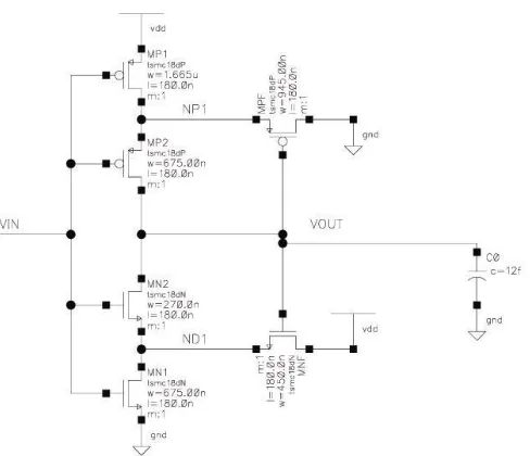
5.1.Description: This circuit is composed of 10 transistors, 6 NMOS and 4 PMOS. A
schematic with nominal transistor sizing is shown in Figure 5.1. The circuit is
controlled by clocking the gate voltages of N6, P1 and P4. During the low phase of
the clock, all internal nodes are pre-charged high through P1 and P4. The rising edge
of the clock begins the evaluation phase, as N6 is turned on and provides a tail
current. During the evaluate phase, the sense-amp detects the polarity of the input
signal and latches the complement to the output. The input pair, N1 and N2,
transforms a differential input voltage into a differential current. The difference in
current between the two sides of the load and the resultant charge imbalance at the
source nodes of N3 and N4 (which are considered the “sense nodes”) causes one of
the output nodes to fall faster than the other. P2, N3, P3, and N4 act as
cross-coupled inverters and provide positive feedback to the output. Once the output
nodes drift far enough apart, the regenerative action of the positive feedback pulls
the high output to VDD and the low output to ground. Just before the regenerative
action begins, N5 begins to conduct, shorting the source nodes of N3 and N4
together. This effectively isolates the regenerative nodes from the input signal. On
the falling edge of the clock, all internal nodes of the amplifier are again pre-charged
high. The regenerative action of this circuit allows it to exponentially amplify very
small signals that have very high bandwidth. The required aperture time is mainly
determined by the capacitance at the output nodes and the conduction of the
5.2.Specific Application: For this example, the sense-amp is used to receive a small
differential pulsed signal from a lossy transmission line. The sense-amp is the
front-end of a sense-amplifier-based flip-flop, therefore the amplifier’s load is the input to
a differential slave latch. Only the approximate input capacitance of the slave latch
is known. The operating specifications are to be as follows:
• Minimum differential input voltage is 200mV peak-to-peak (100mV single-ended
pulse).
• Clock frequency of 1.5GHz. (Assume clock rise time of ~60ps)
• Single-ended external capacitive load of 5fF.
• Common-mode input voltage of 0.9V.
• Average Power Dissipation < 90uW
• Maximum clock-to-output delay of 140ps.
• Nominal aperture time of 200ps
5.3.Advantages of Topology
• The input isolation provided by N5 protects against unwanted changes on the
input data affecting the sense nodes once regeneration begins. [2]
• The gate-isolated topology suffers from less charge injection than other
conventional clocked amplifiers since the input signal is not gated directly to the
sense nodes. When the clock falls, only the tail current is turned off and charge
5.4.Disadvantages of Topology
• This amplifier has a limited common-mode range due to the source-coupled pair.
The input common-mode voltage must be high enough to saturate N1, N2, and N6
for speedy evaluation. In addition, N1 and N2 must be over-driven enough to
completely discharge the output to ground before the end of the evaluation phase.
Low common-mode input will drastically reduce the maximum clock speed. [1]
5.5.Design Approach:
5.5.1. The primary design goal is speed. Therefore the conductance of the
evaluation path should be maximized, while the capacitance is minimized.
However, the sizing must be balanced such that the evaluation path can be
quickly turned off and the output pulled high during the pre-charge phase.
Unlike the source follower design, the complexity of this circuit does not lend
itself to hand analysis using explicit equations for individual transistors.
Instead, an analysis of the function of each transistor and the load each sees and
presents to the circuit is a better tool for finding approximate sizes. The
“fanout-of-4” (FO-4) and 0.11fF per λ of gate width1 approximations are
suitable for the initial analysis. Since each output node drives 5fF of external
load capacitance, the FO-4 approximation shows that the internal capacitance on
the output node should be about 1.25fF. Using the second approximation,
1.25fF equates to approximately 11.4 λ of gate width. This rule of thumb can
now be used as a guide for initial transistor scaling.
5.5.2. Initial Transistor Sizing:
5.5.2.1. P1 and P4 are responsible for pre-charging the internal nodes to a
voltage near VDD in a half clock cycle. Therefore, P1 and P4 must be
large enough to pull the output high before the rising edge of the clock, but
small enough as to not add too much capacitance. Depending on the clock
period, minimum width or 2x minimum width is a good starting point.
5.5.2.2. P2, P3, N3, and N4 make up cross-coupled inverters. N3 and N4 lie in
the evaluation path; therefore their resistance should be as low as possible.
Since P2 and P3 are not in the evaluation path, they mainly add capacitance
to the output. The previous two points show that N3 and N4 should be
large in comparison to P2 and P3. Given the preceding argument, P2 and
P3 can be left minimum sized, and N3 and N4 should be 2x or 3x
minimum sizing to provide strong pull-down.
5.5.2.3. N1, being in series with N3, can be initially sized equal to N3. The
same is true for the N2, N4 pair. Therefore to maintain matching, N1-N4
can be sized and scaled alike.
5.5.2.4. N5 should remain minimum sized to reduce capacitance. Increasing the
width of N5 would negligibly improve its ability to short the sense nodes.
5.5.2.5. N6 should be relatively large to improve current drive and increase
speed. 3x or 4x minimum size is a reasonable starting point.
5.5.2.6. The circuit must remain exactly symmetric to maintain proper operation.
voltage during amplification. The nominal values for gate width are listed
below in Table 5.1.
Table 5.1 - Nominal Gate Widths for Sense-Amplifier
Ref. Designator: N1 N2 N3 N4 N5 N6 P1 P2 P3 P4
Nominal Sizes (um)0.810 0.810 0.810 0.810 0.270 1.080 0.540 0.270 0.270 0.540
5.6.Analysis Setup and Approach: Since the primary goal is speed, only certain
transistors in the circuit were analyzed for performance sensitivity in the following
tests:
5.6.1. The tail transistor, N6, was scaled alone to analyze the effect of changing the
bias current.
5.6.2. N1, N2, N3, and N4 were scaled to analyze the effect of changing the
transconductance of the evaluation path.
5.6.3. N1-N4 and N6 were also scaled together to see the combined effects of the
first two tests.
5.6.4. Finally, P1 and P4 were scaled to analyze the trade-offs between pre-charge
rise-time and added regeneration delay due to increased PMOS loading.
5.7.Sensitivity Analysis
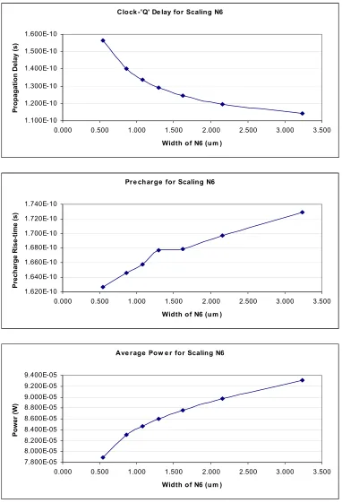
5.7.1. N6 – The tail transistor has a moderate effect on the delay when scaled alone.
Table 5.2 shows that a small improvement in delay can be realized by increasing
the gate width of N6 up to ~180% of its nominal value, with a moderate increase
in power consumption and pre-charge rise-time compared to that seen when
scaling N1-N4 alone. These results show that tweaking the size of N6 with
indicates that scaling N6 beyond 180-200% continues to decrease delay, but
with diminishing returns.
Table 5.2 - Sensitivity Results for Scaling N6
N6
Scaled: 50% 80% Nominal 120% 150% 200% 300%
Gate Width (um) 0.540 0.864 1.080 1.296 1.620 2.160 3.240
Delay 1.564E-10 1.401E-10 1.338E-101.293E-10 1.246E-10 1.195E-10 1.141E-10
Improv. from Nom. -2.260E-11-6.300E-12 4.500E-12 9.200E-12 1.430E-11 1.970E-11
% Change -16.891% -4.709% 3.363% 6.876% 10.688% 14.723%
Prchg. Risetime 1.627E-10 1.646E-10 1.658E-101.677E-10 1.679E-10 1.697E-10 1.729E-10
Improv. from Nom. 3.100E-12 1.200E-12 -1.900E-12-2.100E-12-3.900E-12-7.100E-12
% Change 1.870% 0.724% -1.146% -1.267% -2.352% -4.282%
Avg. Power 7.891E-05 8.304E-05 8.468E-058.598E-05 8.758E-05 8.975E-05 9.314E-05
Improv. from Nom. 5.770E-06 1.640E-06 -1.300E-06-2.900E-06-5.070E-06-8.460E-06
% Change 6.814% 1.937% -1.535% -3.425% -5.987% -9.991%
Figure 5.2 - Sensitivity Results for Scaling N6 Clock -'Q' De lay for Scaling N6
1.100E-10 1.200E-10 1.300E-10 1.400E-10 1.500E-10 1.600E-10
0.000 0.500 1.000 1.500 2.000 2.500 3.000 3.500
Width of N6 (um )
Propagation Delay (s)
Ave r age Pow e r for Scaling N6
7.800E-05 8.000E-05 8.200E-05 8.400E-05 8.600E-05 8.800E-05 9.000E-05 9.200E-05 9.400E-05
0.000 0.500 1.000 1.500 2.000 2.500 3.000 3.500
Width of N6 (um )
Power (W
)
Pr e charge for Scaling N6
1.620E-10 1.640E-10 1.660E-10 1.680E-10 1.700E-10 1.720E-10 1.740E-10
0.000 0.500 1.000 1.500 2.000 2.500 3.000 3.500
Width of N6 (um )
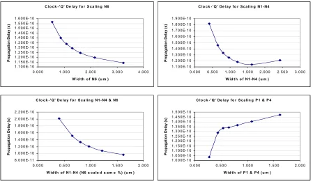
5.7.2. N1-N4 – Since these transistors make up the majority of the evaluation path,
N1-N4 have a greater effect on the delay than does N6 alone, but at a greater
cost in power and particularly pre-charge time due to their direct influence on
the load capacitance. Table 5.3 shows that the decrease in delay when scaling
N1-N4 is almost twice that when scaling N6, but the increase in power and
pre-charge rise-time is approximately 3 and 4 times greater respectively. Figure 5.3
also shows that increasing N1-N4 beyond 200% of their nominal values actually
produces a negative effect on the delay. These numbers show that scaling
N1-N4 alone produces few outstanding positive results.
Table 5.3 - Sensitivity Results for Scaling N1-N4
N1-N4
Scaled: 50% 80% Nominal 120% 150% 200% 300%
Gate Width (um) 0.405 0.648 0.810 0.972 1.215 1.620 2.430
Delay 1.819E-10 1.456E-10 1.334E-101.256E-10 1.185E-10 1.138E-10 1.211E-10
Improv. from Nom. -4.850E-11-1.220E-11 7.800E-12 1.490E-11 1.960E-11 1.230E-11
% Change -36.357% -9.145% 5.847% 11.169% 14.693% 9.220%
Prchg. Risetime 1.471E-10 1.576E-10 1.654E-101.734E-10 1.854E-10 2.056E-10 2.422E-10
Improv. from Nom. 1.830E-11 7.800E-12 -8.000E-12-2.000E-11-4.020E-11-7.680E-11
% Change 11.064% 4.716% -4.837% -12.092% -24.305% -46.433%
Avg. Power 7.380E-05 8.110E-05 8.474E-058.817E-05 9.310E-05 1.014E-04 1.165E-04
Improv. from Nom. 1.094E-05 3.640E-06 -3.430E-06-8.360E-06-1.666E-05-3.176E-05
% Change 12.910% 4.295% -4.048% -9.865% -19.660% -37.479%
Figure 5.3 - Sensitivity Results for Scaling N1-N4 Clock -'Q' De lay for Scaling N1-N4
1.100E-10 1.200E-10 1.300E-10 1.400E-10 1.500E-10 1.600E-10 1.700E-10 1.800E-10 1.900E-10
0.000 0.500 1.000 1.500 2.000 2.500 3.000
Width of N1-N4 (um )
Propagation Delay (s)
Ave rage Pow e r for Scaling N1-N4
7.000E-05 7.500E-05 8.000E-05 8.500E-05 9.000E-05 9.500E-05 1.000E-04 1.050E-04 1.100E-04 1.150E-04 1.200E-04
0.000 0.500 1.000 1.500 2.000 2.500 3.000
Width of N1-N4 (um )
Power (W)
Pre charge for Scaling N1-N4
1.250E-10 1.450E-10 1.650E-10 1.850E-10 2.050E-10 2.250E-10 2.450E-10 2.650E-10
0.000 0.500 1.000 1.500 2.000 2.500 3.000
Width of N1-N4 (um )
5.7.3. N1-N4 & N6 – The results from sections 5.7.1 and 5.7.2 indicate that scaling
N6 or N1-N4 individually produces mediocre results. However, Table 5.4
shows that scaling these five transistors together decreased the delay by the
greatest percentage for a moderate power cost if speed is the primary concern.
Though the pre-charge rise-time still suffers, P1 and P4 can be scaled to balance
the charge and discharge phases and account for the added capacitance of N3
and N4. Figure 5.4 shows that the lowest delay can be achieved in this case,
compared to the cases discussed in the previous two sections.
5.7.4. P1 & P4 – The pre-charge rise-time is very sensitive to scaling P1 and P4,
decreasing by ~14% and 28% for a 20% and 50% increase in gate width
respectively (shown in Table 5.5). However, Figure 5.5 shows that increasing
the width of P1 and P4 beyond 200% of the nominal value produces diminishing
returns and begins to significantly increase the delay due to the added
capacitance. The pre-charge rise-times are compared for all 4 scaling cases in
Figure 5.6.
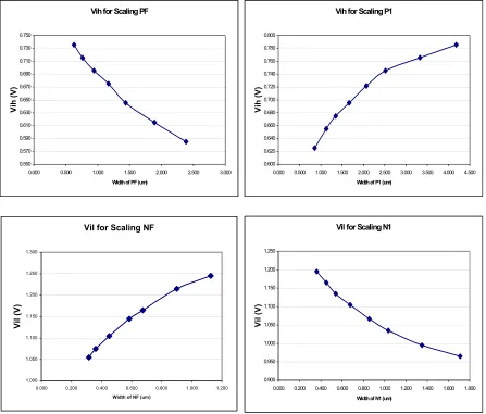
5.7.5. Common-mode (CM) input shift – Though the CM input level is specified at
0.9V, it is important to understand the effects of a change in the CM input
voltage. Below 0.7V, the input transistors are not supplied sufficient over-drive
voltage and the sense-amplifier failed to regenerate the output during the
evaluation phase. If the CM level drifts as low as 0.7V with nominal sizing,
Table 5.6 shows that the delay almost doubles and Figure 5.7a shows that the
increasing the CM level beyond 0.9V continues to decrease the delay, but with
diminishing returns.
Table 5.4 - Sensitivity Results for Scaling N1-N4 & N6
N1-N4 & N6
Scaled: 50% 80% Nominal 120% 150% 200% 300%
Gate Width N1-N4(um)0.405 0.648 0.810 0.972 1.215 1.620 2.430
Gate Width N6 (um) 0.540 0.864 1.080 1.296 1.620 2.160 3.240
Delay 2.016E-10 1.513E-10 1.330E-101.204E-10 1.077E-10 9.600E-11 failed
Improv. from Nom. -6.860E-11-1.830E-11 1.260E-11 2.530E-11 3.700E-11 #VALUE!
% Change -51.579% -13.759% 9.474% 19.023% 27.820% #VALUE!
Prchg. Risetime failed 1.566E-10 1.653E-101.741E-10 1.872E-10 2.088E-10 failed
Improv. from Nom. #VALUE! 8.700E-12 -8.800E-12-2.190E-11-4.350E-11#VALUE!
% Change #VALUE! 5.263% -5.324% -13.249% -26.316% #VALUE!
Avg. Power 6.608E-05 7.941E-05 8.475E-058.953E-05 9.650E-05 1.078E-04 failed
Improv. from Nom. 1.867E-05 5.340E-06 -4.780E-06-1.175E-05-2.305E-05#VALUE!
% Change 22.029% 6.301% -5.640% -13.864% -27.198% #VALUE!
PDP (J) 1.332E-14 1.201E-14 1.127E-141.078E-14 1.039E-14 1.035E-14
Table 5.5 - Sensitivity Results for Scaling P1 & P4
P1 & P4
Scaled: 50% 80% Nominal 120% 150% 200% 300%
Gate Width (um) 0.270 0.432 0.540 0.648 0.810 1.080 1.620
Delay 1.035E-10 1.287E-10 1.336E-101.341E-10 1.366E-10 1.405E-10 1.474E-10
Improv. from Nom. 3.010E-11 4.900E-12 -5.000E-13-3.000E-12-6.900E-12-1.380E-11
% Change 22.530% 3.668% -0.374% -2.246% -5.165% -10.329%
Prchg. Risetime 4.118E-10 1.982E-10 1.671E-101.442E-10 1.200E-10 9.471E-11 6.860E-11
Improv. from Nom. -2.447E-10-3.110E-11 2.290E-11 4.710E-11 7.239E-11 9.850E-11
% Change -146.439% -18.612% 13.704% 28.187% 43.321% 58.947%
Avg. Power 7.887E-05 8.320E-05 8.471E-058.566E-05 8.673E-05 8.831E-05 9.132E-05
Improv. from Nom. 5.840E-06 1.510E-06 -9.500E-07-2.020E-06-3.600E-06-6.610E-06
Figure 5.4 - Sensitivity Results for Scaling N1-N4 & N6 Clock -'Q' De lay for Scaling N1-N4 & N6
8.000E-11 1.000E-10 1.200E-10 1.400E-10 1.600E-10 1.800E-10 2.000E-10 2.200E-10
0.000 0.200 0.400 0.600 0.800 1.000 1.200 1.400 1.600 1.800
Width of N1-N4 (N6 s cale d s am e %) (um )
Propagation Delay (s)
Ave rage Pow e r for Scaling N1-N4 & N6
6.000E-05 7.000E-05 8.000E-05 9.000E-05 1.000E-04 1.100E-04 1.200E-04
0.000 0.200 0.400 0.600 0.800 1.000 1.200 1.400 1.600 1.800
Width of N1-N4 (N6 is s cale d s am e %) (um )
Pow
er (W)
Pre charge for Scaling N1-N4 & N6
1.500E-10 1.600E-10 1.700E-10 1.800E-10 1.900E-10 2.000E-10 2.100E-10 2.200E-10
0.000 0.200 0.400 0.600 0.800 1.000 1.200 1.400 1.600 1.800
Width of N1-N4 (N6 s cale d s am e %) (um )
Figure 5.5 - Sensitivity Results for Scaling P1 & P4 Clock -'Q' De lay for Scaling P1 & P4
1.000E-10 1.100E-10 1.200E-10 1.300E-10 1.400E-10 1.500E-10
0.000 0.200 0.400 0.600 0.800 1.000 1.200 1.400 1.600 1.800
Width of P1 & P4 (um )
Propagation Delay (s)
Ave rage Pow e r for Scaling P1 & P4
7.800E-05 8.000E-05 8.200E-05 8.400E-05 8.600E-05 8.800E-05 9.000E-05 9.200E-05
0.000 0.200 0.400 0.600 0.800 1.000 1.200 1.400 1.600 1.800
Width of P1 & P4 (um )
Power (W)
Pre charge for Scaling P1 & P4
5.000E-11 1.000E-10 1.500E-10 2.000E-10 2.500E-10 3.000E-10 3.500E-10 4.000E-10 4.500E-10
0.000 0.200 0.400 0.600 0.800 1.000 1.200 1.400 1.600 1.800
Width of P1 & P4 (um )
Figure 5.6 - Pre-charge Sensitivity Comparison
Table 5.6 - Delay Sensitivity to Common-mode Input Voltage Shift
Input CM Voltage (V): 0.700 0.800 0.900 1.000 1.100
Delay 2.644E-10 1.74E-10 1.369E-10 1.17E-10 1.049E-10
Improvement from Nom. -1.275E-10 -3.720E-11 2.000E-11 3.200E-11
% Change -93.134% -27.173% Nominal 14.609% 23.375%
Input CM Voltage (V): 1.200 1.300 1.400 1.500 1.600
Delay 9.782E-11 9.393E-11 9.174E-11 9.079E-11 9.077E-11
Improvement from Nom. 3.908E-11 4.297E-11 4.516E-11 4.611E-11 4.613E-11
% Change 28.546% 31.388% 32.988% 33.682% 33.696%
Precharge for Scaling P1 & P4
5.000E-11 1.000E-10 1.500E-10 2.000E-10 2.500E-10 3.000E-10 3.500E-10 4.000E-10 4.500E-10
0.000 0.500 1.000 1.500 2.000
Width of P1 & P4 (um)
Precharge Rise-time (s)
Precharge for Scaling N1-N4
1.250E-10 1.450E-10 1.650E-10 1.850E-10 2.050E-10 2.250E-10 2.450E-10 2.650E-10
0.000 0.500 1.000 1.500 2.000 2.500 3.000
Width of N1-N4 (um)
Precharge Rise-time (s)
Precharge for Scaling N6
1.620E-10 1.640E-10 1.660E-10 1.680E-10 1.700E-10 1.720E-10 1.740E-10
0.000 1.000 2.000 3.000 4.000
Width of N6 (um)
Precharge Rise-time (s)
Precharge for Scaling N1-N4 & N6
1.500E-10 1.600E-10 1.700E-10 1.800E-10 1.900E-10 2.000E-10 2.100E-10 2.200E-10
0.000 0.500 1.000 1.500 2.000
Width of N1-N4 (N6 scaled same%) (um)
Delay vs. Input Common-mode Voltage
0.000E+00 5.000E-11 1.000E-10 1.500E-10 2.000E-10 2.500E-10 3.000E-10
0.600 0.700 0.800 0.900 1.000 1.100 1.200 Vin,CM (V)
Del
ay (s)
Figure 5.7 - Delay Sensitivity to Common-mode Input Voltage Shift
5.7.6. Aperture Time – The nominal aperture time specification of 200ps is
sufficient to swing the sense nodes into regeneration, but a decrease in the time
that the data is stable at the inputs begins to increase the delay as shown in Table
5.7 and Figure 5.8. Aperture times of less than 50ps are not sufficient to
regenerate the output, which can be seen in Figure 5.8a.
Table 5.7 - Delay Sensitivity to Allowed Aperture Time
Aperture Time 5.000E-11 7.500E-11 1.000E-10 1.500E-10 5.000E-10
Delay 1.714E-10 1.494E-10 1.418E-10 1.373E-10 1.369E-10
Improvement from Nom. -3.450E-11 -1.250E-11 -4.900E-12 -4.000E-13
% Change -25.20% -9.13% -3.58% -0.29% Nominal
(measured from 50% point of CLK to 50% point of Data)
Delay vs. Aperture Time
1.300E-10 1.350E-10 1.400E-10 1.450E-10 1.500E-10 1.550E-10 1.600E-10 1.650E-10 1.700E-10 1.750E-10
0.000E+00 1.000E-10 2.000E-10 3.000E-10 4.000E-10 5.000E-10 6.000E-10
Delay (s)
Aperture Time (s)
Figure 5.8a - Single-Ended Transient Response Plots for Aperture Time Sweep
5.8.Key Considerations
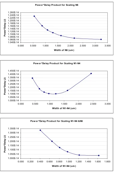
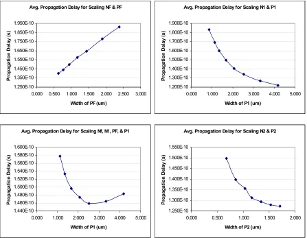
5.8.1. Power-Delay Product (PDP) – As with most digital circuits, there is a
significant trade-off between power and delay. The delay results for all four of
scaling cases are presented together for comparison in Figure 5.9. Likewise, the
power results are presented together in Figure 5.10. However, Figure 5.11,
which shows the power-delay product for scaling N1-N4 and & N6 together and
separately, best illustrates the power-delay trade-off. The three graphs show that
N6 is the key to minimizing PDP, but that scaling beyond 200% of the nominal
Figure 5.9 - Clock-to-Output Sensitivity Comparison
Figure 5.10 - Average Power Comparison C lo c k - 'Q ' De lay f o r S ca lin g N6
1 .1 0 0E- 1 0 1 .1 5 0E- 1 0 1 .2 0 0E- 1 0 1 .2 5 0E- 1 0 1 .3 0 0E- 1 0 1 .3 5 0E- 1 0 1 .4 0 0E- 1 0 1 .4 5 0E- 1 0 1 .5 0 0E- 1 0 1 .5 5 0E- 1 0 1 .6 0 0E- 1 0
0.00 0 1 .0 0 0 2 .0 00 3.00 0 4.00 0
W id t h o f N6 ( u m )
P ropagat ion D e la y ( s )
C lo c k - 'Q ' De lay f o r S ca lin g N1 - N4
1 .1 0 0E- 1 0 1 .2 0 0E- 1 0 1 .3 0 0E- 1 0 1 .4 0 0E- 1 0 1 .5 0 0E- 1 0 1 .6 0 0E- 1 0 1 .7 0 0E- 1 0 1 .8 0 0E- 1 0 1 .9 0 0E- 1 0
0.00 0 0 .5 00 1.00 0 1 .5 00 2.00 0 2 .5 00 3.00 0
W id t h o f N1 - N4 ( u m )
P ropagat ion D e la y ( s )
C lo c k - 'Q ' De lay f o r S ca lin g N1 - N4 & N6
8 .0 0 0E- 1 1 1 .0 0 0E- 1 0 1 .2 0 0E- 1 0 1 .4 0 0E- 1 0 1 .6 0 0E- 1 0 1 .8 0 0E- 1 0 2 .0 0 0E- 1 0 2 .2 0 0E- 1 0
0.00 0 0 .5 0 0 1 .0 00 1.50 0 2.00 0
W id t h o f N1 - N4 ( N6 s c a le d s am e % ) ( u m )
P ropagat ion D e la y ( s )
C lo c k - 'Q ' De lay f o r S ca lin g P1 & P4
1 .0 0 0E- 1 0 1 .0 5 0E- 1 0 1 .1 0 0E- 1 0 1 .1 5 0E- 1 0 1 .2 0 0E- 1 0 1 .2 5 0E- 1 0 1 .3 0 0E- 1 0 1 .3 5 0E- 1 0 1 .4 0 0E- 1 0 1 .4 5 0E- 1 0 1 .5 0 0E- 1 0
0.00 0 0 .5 0 0 1 .0 00 1.50 0 2.00 0
W id t h o f P1 & P4 ( u m )
P ropagat ion D e la y ( s )
A ve r ag e Po w e r fo r Scalin g N6
7.800E-05 8.000E-05 8.200E-05 8.400E-05 8.600E-05 8.800E-05 9.000E-05 9.200E-05 9.400E-05
0.000 1.000 2.000 3.000 4.000 W id th o f N6 (u m )
Pow
er (W
)
A ve r ag e Po w e r fo r Scalin g N1-N4
7.000E-05 7.500E-05 8.000E-05 8.500E-05 9.000E-05 9.500E-05 1.000E-04 1.050E-04 1.100E-04 1.150E-04 1.200E-04
0.000 0.500 1.000 1.500 2.000 2.500 3.000 W id th o f N1-N4 (u m )
Pow
er (W
)
A ve r ag e Po w e r fo r Scalin g N1-N4 & N6
6.000E-05 7.000E-05 8.000E-05 9.000E-05 1.000E-04 1.100E-04 1.200E-04
0.000 0.500 1.000 1.500 2.000 W id th o f N1-N4 (N6 is s cale d s am e %) (u m )
Pow
er (W
)
A ve r ag e Po w e r fo r Scalin g P1 & P4
7.800E-05 8.000E-05 8.200E-05 8.400E-05 8.600E-05 8.800E-05 9.000E-05 9.200E-05
0.000 0.500 1.000 1.500 2.000 W id th o f P1 & P4 (u m )
Pow
er (W
Figure 5.11 – Power-Delay Product Sensitivity Comparison Pow e r*De lay Product for Scaling N1-N4 &N6
1.000E-14 1.050E-14 1.100E-14 1.150E-14 1.200E-14 1.250E-14 1.300E-14 1.350E-14
0.000 0.200 0.400 0.600 0.800 1.000 1.200 1.400 1.600 1.800
Width of N1-N4 (um )
Power*Delay (J)
Pow e r*De lay Product for Scaling N1-N4
1.000E-14 1.050E-14 1.100E-14 1.150E-14 1.200E-14 1.250E-14 1.300E-14 1.350E-14 1.400E-14 1.450E-14
0.000 0.500 1.000 1.500 2.000 2.500 3.000
Width of N1-N4 (um )
Power*Delay (J)
Pow e r*De lay Product for Scaling N6
1.040E-14 1.060E-14 1.080E-14 1.100E-14 1.120E-14 1.140E-14 1.160E-14 1.180E-14 1.200E-14 1.220E-14 1.240E-14 1.260E-14
0.000 0.500 1.000 1.500 2.000 2.500 3.000 3.500
Width of N6 (um )
Power*Del
ay (
5.8.2. Elmore Delay – Though not explored in this analysis, transistors N3 and N4
could be scaled separately from N1 and N2 to examine benefits from optimizing
the Elmore delay in the evaluation path. Adjusting the ratio of N3 to N1
(likewise for N4 to N2) to keep the same low series resistance, but lower the
capacitance closest to the output nodes, would likely further reduce the delay.
5.8.3. Phase Balancing – Though delay minimization is key, the sizing of the
pull-down transistor with respect to the pre-charge transistors is important to ensure
that all internal nodes are completely pre-charged and avoid offset on the sense
nodes. If the sense nodes do not pre-charge to the same voltage, the
regeneration of the differential input voltage is corrupted due to the imbalanced
6. Schmidt Trigger Design Example
6.1.Description: This circuit is essentially an inverter with differing positive and
negative switching thresholds, though it requires 3 times the number of transistors as
a simple inverter. A Schmidt trigger employs positive feedback to increase the
threshold at which the output switches for rising inputs and decrease the threshold at
which the output switches for falling inputs. The difference between the threshold
for a low-to-high transition (VIL) and the threshold for a high-to-low transition (VIH)
is called the hysteresis voltage (VHYS = VIL - VIH). A major advantage of separating
the positive and negative thresholds is the ability to reduce unwanted switching due
to a noisy input signal wandering at mid-level1. There are several Schmidt trigger
topologies, but this example focuses on the circuit in Figure 6.1. Transistors NF and
PF provide the positive feedback that ultimately controls the values for VHYS .
Figure 6.1 - Schmidt Trigger Schematic w/ Nominal Sizes
6.2.Specific Application: For this example, a Schmidt trigger will be used to clean up a
noisy digital signal before it is to be driven off chip. These signals have become
ridden with glitches and lost edge-rate due to having traveled a considerable distance
across chip. The waveform must be cleaned up before it is buffered off-chip. The
estimated external capacitive load is 12fF, which is the approximate input
capacitance of a 2.5x sized inverter. The operating specifications are to be as
follows:
• Clock frequency of 1.5GHz. (Assume clock rise time of ~60ps)
• Full-swing (0-1.8V) digital input signal
• Single-ended external capacitive load of 12fF.
• VHYS = 400mV, with VIH = 700mV and VIL =1.1V
• Average Power Dissipation < 300uW
• Maximum Propagation Delay2,Tp = 0.5*[TPHL + TPLH]= 150ps
6.3.Advantages of Topology
• The hysteresis added by moving both the positive and the negative thresholds
increases the noise margin of both the high and the low states. This is superior to
hysteresis added in an inverter, where only one state’s noise margin can be
increased at the expense of the opposite state. Specific benefits include:
• Protecting against high signals glitching low, and low signals glitching
high.
• Removing ringing in steady-state