LTC4353
1
4353fTypical applicaTion
FeaTures
DescripTion
Dual Low Voltage
Ideal Diode Controller
The LTC®4353 controls external N-channel MOSFETs to
implement an ideal diode function. It replaces two high power Schottky diodes and their associated heat sinks, saving power and board area. The ideal diode function permits low loss power supply ORing and supply holdup applications.
The LTC4353 regulates the forward-voltage drop across the MOSFET to ensure smooth current transfer in diode-OR applications. A fast turn-on reduces the load voltage droop during supply switchover. If the input supply fails or is shorted, a fast turn-off minimizes reverse-current transients.
The controller operates with supplies from 2.9V to 18V. If both supplies are below 2.9V, an external supply is needed at the VCC pin. Enable inputs can be used to turn off the MOSFET and put the controller in a low current state. Status outputs indicate whether the MOSFETs are on or off.
2.9V to 18V, 10A Ideal Diode-OR Output Maintained with Failing Input Supply
applicaTions
n Low Loss Replacement for Power Diodes n Controls N-Channel MOSFETs
n 0V to 18V Supply ORing or Holdup n 1µs Gate Turn-On and Turn-Off Time n Enable Inputs
n MOSFET On-Status Outputs
n 16-Lead MSOP and DFN (4mm × 3mm) Packages
n Redundant Power Supplies n Supply Holdup
n High Availability Systems and Servers n Telecom and Network Infrastructure
L, LT, LTC, LTM, Linear Technology and the Linear logo are registered trademarks and
Hot Swap, PowerPath and ThinSOT are trademarks of Linear Technology Corporation. All other trademarks are the property of their respective owners. Protected by U.S. Patents, including 7920013 and 8022679. Si4126DY Si4126DY GATE1 CPO1 CPO2 GND EN1 EN2 4353 TA01a 2.9V TO 18V 2.9V TO 18V
*OPTIONAL FOR FAST TURN-ON
0.1µF V10AOUT 56nF* 56nF* VIN1 VCC ONST1 ONST2 OUT1 OUT2 MOSFET ON-STATUS OUTPUTS GATE2 VIN2 LTC4353 5µs/DIV VOL TAGE 2V /DIV 4353 TA01b VIN1 = 5.2V VIN2 = 5V IL = 8A CL = 100µF VIN1 VIN2 VOUT
LTC4353
2
4353fabsoluTe MaxiMuM raTings
VIN1, VIN2, OUT1, OUT2 Voltages ...−2V to 24V VCC Voltage ... −0.3V to 6.5V GATE1, GATE2 Voltages (Note 3) ... −0.3V to 34V CPO1, CPO2 Voltages (Note 3) ... −0.3V to 34V EN1, EN2, ONST1, ONST2 Voltages ...−0.3V to 24V CPO1, CPO2 Average Current ...10mA ONST1, ONST2 Currents ...5mA
(Notes 1, 2)
orDer inForMaTion
LEAD FREE FINISH TAPE AND REEL PART MARKING* PACKAGE DESCRIPTION TEMPERATURE RANGE
LTC4353CDE#PBF LTC4353CDE#TRPBF 4353 16-Pin (4mm × 3mm) Plastic DFN 0°C to 70°C
LTC4353IDE#PBF LTC4353IDE#TRPBF 4353 16-Pin (4mm × 3mm) Plastic DFN –40°C to 85°C
LTC4353CMS#PBF LTC4353CMS#TRPBF 4353 16-Pin Plastic MSOP 0°C to 70°C
LTC4353IMS#PBF LTC4353IMS#TRPBF 4353 16-Pin Plastic MSOP –40°C to 85°C
Consult LTC Marketing for parts specified with wider operating temperature ranges. *The temperature grade is identified by a label on the shipping container. For more information on lead free part marking, go to: http://www.linear.com/leadfree/
For more information on tape and reel specifications, go to: http://www.linear.com/tapeandreel/ 16 15 14 13 12 11 10 9 17 1 2 3 4 5 6 7 8 EN1 GND VCC VIN1 GATE1 CPO1 OUT1 ONST1 EN2 NC NC VIN2 GATE2 CPO2 OUT2 ONST2 TOP VIEW DE PACKAGE 16-LEAD (4mm × 3mm) PLASTIC DFN TJMAX = 125°C, θJA = 43°C/W
EXPOSED PAD (PIN 17) PCB GND CONNECTION OPTIONAL
1 2 3 4 5 6 7 8 EN2 NC NC VIN2 GATE2 CPO2 OUT2 ONST2 16 15 14 13 12 11 10 9 EN1 GND VCC VIN1 GATE1 CPO1 OUT1 ONST1 TOP VIEW MS PACKAGE 16-LEAD PLASTIC MSOP TJMAX = 125°C, θJA = 125°C/W
pin conFiguraTion
Operating Ambient Temperature Range
LTC4353C ... 0°C to 70°C LTC4353I ...−40°C to 85°C Storage Temperature Range ... −65°C to 150°C Lead Temperature (Soldering, 10 sec)
LTC4353
3
4353felecTrical characTerisTics
Note 1: Stresses beyond those listed under Absolute Maximum Ratings may cause permanent damage to the device. Exposure to any Absolute Maximum Rating condition for extended periods may affect device reliability and lifetime.
Note 2: All currents into device pins are positive; all currents out of device pins are negative. All voltages are referenced to GND unless otherwise specified.
SYMBOL PARAMETER CONDITIONS MIN TYP MAX UNITS
Supplies
VIN VIN1, VIN2 Operating Range
With External VCC Supply
l l 2.9 0 V18 CC V V
VCC(EXT) VCC External Supply Operating Range VIN1, VIN2 ≤ VCC l 2.9 6 V
VCC(REG) VCC Regulated Voltage l 4.5 5 5.5 V
IIN VIN1, VIN2 Current
Enabled, Higher Supply Enabled, Lower Supply Pull-Up Disabled Other VIN = 11.7V, Both EN = 0V Other VIN = 12.3V, Both EN = 0V Both VIN = 0V, VCC = 5V, Both EN = 0V Both EN = 1V l l l l 1.5 200 –45 75 2.5 300 –80 160 mA µA µA µA ICC VCC Current Enabled
Disabled VVCCCC = 5V, Both V = 5V, Both VININ = 1.2V, Both = 1.2V, Both ENEN = 0V = 1V l l
1.5
88 1902.2 mA µA
VCC(UVLO) VCC Undervoltage Lockout Threshold VCC Rising l 2.3 2.55 2.7 V
ΔVCC(HYST) VCC Undervoltage Lockout Hysteresis l 40 120 300 mV
Ideal Diode Control
VFR Forward Regulation Voltage (VIN − OUT) VIN = 1.2V, VCC = 5V
VIN = 12V
l l
2
2 12 25 25 50 mV mV
ΔVGATE MOSFET Gate Drive (GATE – VIN) VFWD = 0.2V; I = 0, −1μA; Highest VIN =12V
VFWD = 0.2V; I = 0, −1μA; Highest VIN =2.9V l l
10
4.5 12 7 14 9 V V
tON(GATE) GATE1, GATE2 Turn-On Propagation Delay VFWD (= VIN – OUT) Step: −0.3V to 0.3V l 0.4 1 µs
tOFF(GATE) GATE1, GATE2 Turn-Off Propagation Delay VFWD Step: 0.3V to −0.3V l 0.3 1 µs
IGATE GATE1, GATE2 Fast Pull-Up Current
GATE1, GATE2 Fast Pull-Down Current GATE1, GATE2 Off Pull-Down Current
VFWD = 0.4V, ΔVGATE = 0V, CPO = 17V VFWD = −0.8V, ΔVGATE = 5V Corresponding EN = 1V, ΔVGATE = 2.5V l l l –0.9 0.9 65 –1.4 1.4 110 –1.9 1.9 160 A A µA Input/Output Pins
VEN(TH) EN1, EN2 Threshold Voltage EN Falling l 580 600 620 mV
ΔVEN(TH) EN1, EN2 Threshold Hysteresis l 2 8 20 mV
IEN EN1, EN2 Current At 0.6V l 0 ±1 µA
IOUT OUT1, OUT2 Current
Enabled
Disabled OUTn = 0V, 12V; Both Both EN = 1V EN = 0V
l l
–4
8 160 16 µA µA
ICPO(UP) CPO1, CPO2 Pull-Up Current CPO = VIN l –40 –70 –115 µA
VOL ONST1, ONST2 Output Low Voltage I = 1mA
I = 3mA
l l
0.14
0.42 0.4 1.2 V V VOH ONST1, ONST2 Output High Voltage I = −1μA l VCC – 1.4 VCC – 0.9 VCC – 0.5 V
IONST ONST1, ONST2 Leakage Current At 12V l 0 ±1 µA
ΔVGATE(ON) MOSFET On-Detect Threshold (GATE – VIN) ONST Pulls Low l 0.28 0.7 1.1 V
The l denotes those specifications which apply over the full operating
temperature range, otherwise specifications are at TA = 25°C. VIN1 = VIN2 = 12V, OUT = VIN, VCC Open, unless otherwise noted.
Note 3: Internal clamps limit the GATE and CPO pins to a minimum of 10V above, and a diode below the corresponding VIN pin. Driving these pins to
LTC4353
4
4353fTA = 25°C, VIN1 = VIN2 = 12V, OUT = VIN, VCC open,
unless otherwise noted.
Typical perForMance characTerisTics
OUT Current vs Voltage Forward Regulation Voltage vs VIN Voltage with External VCC �VGATE Voltage vs Current
�VGATE and VCC Voltages
vs VIN Voltage
ONST Output Low Voltage
vs Current ONSTvs Current Output High Voltage VIN Current vs Voltage
VIN Current vs Voltage with
External VCC VCC Current vs Voltage
VIN (V) 0 –0.5 0 1.5 3 6 9 12 15 0.5 2.0 1.0 2.5 18 4353 G01 IIN (mA) OTHER VIN = 0V OTHER VIN = 12V VIN (V) 4353 G02 IIN (µA) 0 0 150 250 1 2 3 4 5 50 –50 100 200 6 VCC = 6V OTHER VIN = 0V 0 0.25 1.00 1.75 0.50 1.25 0.75 1.50 4353 G03 VCC (V) 0 1 2 3 4 5 6 ICC (mA) BOTH VIN = 0V 4 14 0 6 2 10 12 8 VIN (V) 0 3 6 9 12 15 18 4353 G07 VCC VGA TE – V IN , VCC (V) ∆VGATE VIN (V) 0 0 15 30 1 2 3 4 5 20 10 25 5 4353 G05 VCC = 5V VFR (mV) VCC = 3.3V VOUT (V) 4353 G04 IOUT (µA) 0 0 150 250 3 6 9 12 15 50 –50 100 200 18 IGATE (µA) 0 –20 –40 –60 –80 –100 –120 4353 G06 VGA TE – V IN (V) VIN = 18V –2 0 2 8 14 4 10 6 12 OUT = VIN – 0.1V VIN = 2.9V IONST (mA) 0 0 600 1 2 3 4 800 200 400 5 4353 G08 VOL (mV) IONST (µA) 0 0 3 –2 –4 –6 –8 5 1 4 2 –10 4353 G09 VOH (V)
LTC4353
5
4353fTA = 25°C, VIN1 = VIN2 = 12V, OUT = VIN, VCC open,
unless otherwise noted.
Typical perForMance characTerisTics
Start-Up Waveform on VIN1
Power-Up Fast Gate Switchover From Failing Supply
pin FuncTions
CPO1, CPO2: Charge Pump Output. Connect a capacitor
from this pin to the corresponding VIN pin. The value of this capacitor should be approximately 10× the gate ca-pacitance (CISS) of the MOSFET switch. The charge stored on this capacitor is used to pull-up the gate during a fast turn-on. Leave this pin open if fast turn-on is not needed.
EN1, EN2: Enable Input. Keep this pin below 0.6V to
en-able diode control on the corresponding supply. Driving this pin high shuts off the MOSFET gate (current can still flow through its body diode). The comparator has a built-in hysteresis of 8mV. Having both EN pins high lowers the current consumption of the controller.
Exposed Pad (DE Package Only): This pin may be left
open or connected to device ground.
GATE1, GATE2: MOSFET Gate Drive Output. Connect this
pin to the gate of the external N-channel MOSFET switch. An internal clamp limits the gate voltage to 12V above, and a diode below the input supply. During fast turn-on, a 1.4A pull-up current charges GATE from CPO. During fast turn-off, a 1.4A pull-down current discharges GATE to VIN.
GND: Device Ground.
ONST1, ONST2: MOSFET Status Output. This pin is pulled
low by an internal switch when GATE is more than 0.7V above VIN to indicate an on MOSFET. An internal 500k resistor pulls this pin up to a diode below VCC. It may be pulled above VCC using an external pull-up. Tie to GND or leave open if unused.
OUT1, OUT2: Output Voltage Sense Input. Connect this
pin to the load side of the MOSFET. The voltage sensed at this pin is used to control the MOSFET gate.
VCC: Low Voltage Supply. Connect a 0.1μF capacitor from
this pin to ground. For VIN ≥ 2.9V, this pin provides decou-pling for an internal regulator that generates a 5V supply. For applications where both VIN < 2.9V, also connect an external supply voltage in the 2.9V to 6V range to this pin.
VIN1, VIN2: Voltage Sense and Supply Input. Connect
this pin to the supply side of the MOSFET. The low volt-age supply VCC is generated from the higher of VIN1 and VIN2. The voltage sensed at this pin is used to control the MOSFET gate. 5ms/DIV VOL TAGE 5V /DIV 4353 G10 VIN1 VCC OUT CPO1 CPO2 GATE1 5µs/DIV 4353 G11 ∆VGATE2 10V/DIV ∆VGATE1 5V/DIV VIN2 2V/DIV VIN1 2V/DIV VIN1 = 5.2V VIN2 = 5V CL = 100µF IL = 8A
LTC4353
6
4353fFuncTional DiagraM
4353 BD CHARGE PUMP1 f = 3MHz LDO CHARGE PUMP2 f = 3MHz*DE PACKAGE ONLY
GATE1 OFF GATE2 OFF – + SA1 – + – + – + – + 11 CPO1 12 GATE1 13 VIN1 VFR1 VFR2 VCC VCC LOW GATE1 VIN2 VIN1 10 9 8 OUT1 ONST1 500k CP4 CP2 CP1 CP3 0.7V 0.6V 0.6V 2.55V VIN1 CPO2 GATE2 17 EXPOSED PAD* GND VIN2 OUT2 – + – + VCC GATE2 ONST2 500k CP5 0.7V VIN2 DISABLE1 DISABLE2 1 EN2 14VCC 16EN1 Z 6 5 15 4 7 +– + – + – + – SA2
LTC4353
7
4353foperaTion
The LTC4353 controls N-channel MOSFETs to emulate two ideal diodes. When enabled, each servo amplifier (SA1, SA2) controls the gate of the external MOSFET to servo its forward voltage drop (VFWD = VIN – OUT) to VFR. The gate voltage rises to enhance the MOSFET if the load current causes the drop to exceed VFR. For large output currents, the MOSFET gate is driven fully on and the volt-age drop is equal to IFET • RDS(ON).
In the case of an input supply short-circuit, when the MOSFET is conducting, a large reverse current starts flowing from the load towards the input. SA detects this failure condition as soon as it appears, and turns off the MOSFET by rapidly pulling down its gate.
SA quickly pulls up the gate whenever it senses a large for-ward voltage drop. An external capacitor between the CPO and VIN pins is needed for fast gate pull-up. This capacitor
is charged up, at device power-up, by the internal charge pump. The stored charge is used for the fast gate pull-up. The GATE pin sources current from the CPO pin and sinks current to the VIN and GND pins. Clamps limit the GATE and CPO voltages to 12V above and a diode below VIN. Internal switches pull the ONST pins low when the GATE to VIN voltage exceeds 0.7V to indicate that power is passing through the MOSFET.
LDO is a low dropout regulator that generates a 5V supply at the VCC pin from the highest VIN input. When both VIN are below 2.9V, an external supply in the 2.9V to 6V range is required at the VCC pin.
VCC and EN pin comparators, CP1 to CP3, control power passage. The MOSFET is held off whenever the EN pin is above 0.6V, or the VCC pin is below 2.55V. A high on both EN pins lowers the current consumption of the device.
LTC4353
8
4353fHigh availability systems often employ parallel connected power supplies or battery feeds to achieve redundancy and enhance system reliability. ORing diodes have been a popular means of connecting these supplies at the point of load. Diodes followed by storage capacitors also hold up supply voltages when an input voltage sags or has a brownout. The disadvantage of these approaches is the diode’s significant forward-voltage drop and the result-ing power loss. The LTC4353 solves these problems by using an external N-channel MOSFET as the pass element (see Figure 1). The MOSFET is turned on when power is being passed, allowing for a low voltage drop from the supply to the load. When the input source voltage drops below the output common supply voltage it turns off the MOSFET, thereby matching the function and performance of an ideal diode.
applicaTions inForMaTion
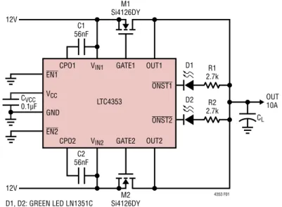
Figure 1. 12V Ideal Diode-OR with Status Lights
Figure 2. Power Supply Configurations
Power Supply Configuration
The LTC4353 can operate with input supplies down to 0V. This requires powering the VCC pin with an early external supply in the 2.9V to 6V range. In this range of operation VIN should be lower than VCC. If VCC powers up after VIN and backfeeding of VCC by the internal 5V LDO is a concern, then a series resistor (few 100Ω) or Schottky diode limits device power dissipation and backfeeding of a low VCC supply when any VIN is high. A 0.1µF bypass capacitor should also be connected between the VCC and GND pins, close to the device. Figure 2 illustrates this. If either VIN operates above 2.9V, the external supply at VCC is not needed. The 0.1µF capacitor is still required for bypassing. GATE1 4353 F02 0V TO VCC 0V TOVCC VIN1 VCC GATE2 VIN2 LTC4353 2.9V TO 6V GATE1 M1 M2 M1 M2 2.9V TO 18V (0V TO 18V) 0V TO 18V (2.9V TO 18V) VIN1 VCC GATE2 VIN2 LTC4353 CVCC 0.1µF CVCC 0.1µF OPTIONAL OR HERE M1 Si4126DY M2 Si4126DY GATE1 CPO1 CPO2 GND EN1 EN2 4353 F01 12V 12V D1, D2: GREEN LED LN1351C CVCC 0.1µF OUT10A C1 56nF R1 2.7k C2 56nF VIN1 VCC ONST1 ONST2 OUT1 OUT2 D1 D2 GATE2 VIN2 LTC4353 R2 2.7k CL
LTC4353
9
4353fMOSFET Selection
The LTC4353 drives N-channel MOSFETs to conduct the load current. The important features of the MOSFET are its maximum drain-source voltage BVDSS, maximum gate-source voltage VGS(MAX), and the on-resistance RDS(ON). If an input is connected to ground, the full supply voltage can appear across the MOSFET. To survive this, the BVDSS must be higher than the supply voltages. The VGS(MAX) rating of the MOSFET should exceed 14V since that is the upper limit of the internal GATE to VIN clamp. The RDS(ON) of the MOSFET dictates the maximum voltage drop (IL • RDS(ON)) and the power dissipated (IL2 • RDS(ON)) in the MOSFET. Note that the minimum MOSFET voltage drop is controlled by the servo amplifier regulation volt-age, hence, picking a very low RDS(ON) (below VFR/IL) may not be beneficial.
CPO Capacitor Selection
The recommended value of the capacitor between the CPO and VIN pins is approximately 10× the input capacitance CISS of the MOSFET. A larger capacitor takes a cor-respondingly longer time to be charged by the internal charge pump. A smaller capacitor suffers more voltage drop during a fast gate turn-on event as it shares charge with the MOSFET gate capacitance.
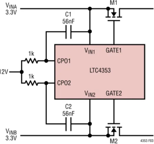
External CPO Supply
The internal charge pump takes milliseconds to charge up the CPO capacitor especially during device power-up. This time can be shortened by connecting an external supply to the CPO pin. A series resistor is needed to limit the current into the internal clamp between CPO and VIN pins. The CPO supply should also be higher than the main input supply to meet the gate drive requirements of the MOSFET. Figure 3 shows such a 3.3V ideal diode application, where a 12V supply is connected to the CPO pins through a 1k resistor. The 1k limits the current into the CPO pin, when the VIN pin is grounded. For the 8.7V gate drive (12V – 3.3V), logic-level MOSFETs would be an appropriate choice for M1 and M2.
Input Transient Protection
When the capacitances at the input and output are very small, rapid changes in current can cause transients that exceed the 24V absolute maximum rating of the VIN and OUT pins. In ORing applications, one surge suppressor connected from OUT to ground clamps all the inputs. In the absence of a surge suppressor, an output capacitance of 10μF is sufficient in most applications to prevent the transient from exceeding 24V.
Figure 3. 3.3V Ideal Diode with External 12V Supply Powering CPO for Faster Start-Up and Refresh
M1 M2 GATE1 4353 F03 VINA 3.3V VINB 3.3V VIN1 GATE2 VIN2 LTC4353 CPO1 CPO2 12V 1k 1k C1 56nF C2 56nF
applicaTions inForMaTion
LTC4353
10
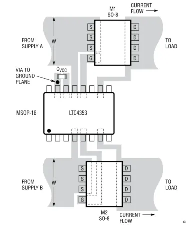
4353fFigure 4. Recommended PCB Layout for M1, M2, CVCC
applicaTions inForMaTion
Design Example
The following design example demonstrates the calcula-tions involved for selecting components in a 12V system with 10A maximum load current (see Figure 1).
First, calculate the RDS(ON) of the MOSFET to achieve the desired forward drop at full load. Assuming a VDROP of 30mV:
RDS(ON)≤ VDROP
ILOAD = 30mV
10A = 3mΩ
The Si4126DY offers a good solution in a SO-8 sized package with a 2.8mΩ maximum RDS(ON), 30V BVDSS, and 20V VGS(MAX). The maximum power dissipation in the MOSFET is:
P = I2LOAD • RDS(ON) = (10A)2 • 2.8mΩ = 0.3W With a maximum steady-state thermal resistance θJA
of 35°C/W, 0.3W causes a modest 11°C rise in junction temperature of the Si4126DY above the ambient.
The input capacitance, CISS, of the Si4126DY is about 5500pF. Following the 10× recommendation, a 56nF capacitor is selected for C1 and C2.
LEDs, D1 and D2, require around 3mA for good luminous intensity. Accounting for a 2V diode drop and 0.6V VOL, R1 and R2 are set to 2.7k.
PCB Layout Considerations
Connect the VIN and OUT pin traces as close as possible to the MOSFET’s terminals. Keep the traces to the MOS-FET wide and short to minimize resistive losses. The PCB traces associated with the power path through the MOSFET should have low resistance (see Figure 4).
It is also important to put CVCC, the bypass capacitor for the VCC pin, as close as possible between VCC and GND. Place C1 and C2 near the CPO and VIN pins. Surge sup-pressors, when used, should be mounted close to the LTC4353 using short lead lengths.
4353 F04 MSOP-16 W CURRENT FLOW VIA TO GROUND PLANE S S S G D D D D M2 SO-8 TO LOAD FROM SUPPLY B W CURRENT FLOW S S S G D D D D M1 SO-8 TO LOAD FROM SUPPLY A CVCC TRACK WIDTH W: 0.03 PER AMPERE ON 1oz Cu FOIL
DRAWING IS NOT TO SCALE!
LTC4353
11
4353fTypical applicaTions
12V Supply with Capacitive Reservoir for Data Backup on Power Fail for Disk Drive and Solid-State Drive Applications
3.3V Main and Auxiliary Supply Diode-OR (Auxiliary Ideal Diode Disabled if Main Above 2.95V)
M1 Si4126DY M2 Si4126DY GATE1 CPO1 CPO2 GND EN1 EN2 4353 TA02 12V CVCC 0.1µF STORAGEDEVICE C1 56nF C2 56nF VIN1 VCC ONST1 ONST2 OUT1 OUT2 GATE2 VIN2 LTC4353 RCHRG 1k BUCK REG. CRESV 3F
CRESV: 3 PARALLEL STRINGS, EACH WITH 3 SERIES PM-5R0V305-R
M1 Si4126DY M2 Si4126DY GATE1 CPO1 CPO2 GND EN1 EN2 4353 TA03 3.3V MAIN 3.3V AUX CVCC 0.1µF OUT C1 56nF C2 56nF VIN1 VCC ONST1 ONST2 OUT1 OUT2 GATE2 VIN2 LTC4353 R3 39.2k R4 10k
LTC4353
12
4353fPlug-in Card Supply Holdup Using Ideal Diode at 12V and 3.3V Inputs
PLUG-IN CARD CONNECTORS BACKPLANE 4353 TA04 12V 3.3V M1 Si4126DY M2 Si4126DY GATE1 CPO1 CPO2 C2 56nF NC VIN1 OUT1 OUT2 GATE2 VIN2 LTC4353 CHOLDUP1 3.3VOUT 12VOUT + CHOLDUP2 +
Typical applicaTions
LTC4353
13
4353fTypical applicaTions
Redundant Power Supply System with ORing on Backplane, as in MicroTCA
LOAD CARD 2
POWER SUPPLY MODULE 1
4353 TA05 LOAD CARD 1 12V Si4126DY Si4126DY GATE1 CPO1 CPO2 GND EN1 EN2 NC NC 0.1µF VIN1 VCC ONST1 ONST2 OUT1 OUT2 GATE2 VIN2 LTC4353
POWER SUPPLY MODULE 2
12V Si4126DY Si4126DY GATE1 CPO1 CPO2 GND EN1 EN2 NC NC 0.1µF VIN1 VCC ONST1 ONST2 OUT1 OUT2 GATE2 VIN2 LTC4353
LTC4353
14
4353fpackage DescripTion
Please refer to http://www.linear.com/designtools/packaging/ for the most recent package drawings.
3.00 ±0.10 (2 SIDES) 4.00 ±0.10
(2 SIDES)
NOTE:
1. DRAWING PROPOSED TO BE MADE VARIATION OF VERSION (WGED-3) IN JEDEC PACKAGE OUTLINE MO-229
2. DRAWING NOT TO SCALE
3. ALL DIMENSIONS ARE IN MILLIMETERS
4. DIMENSIONS OF EXPOSED PAD ON BOTTOM OF PACKAGE DO NOT INCLUDE MOLD FLASH. MOLD FLASH, IF PRESENT, SHALL NOT EXCEED 0.15mm ON ANY SIDE 5. EXPOSED PAD SHALL BE SOLDER PLATED
6. SHADED AREA IS ONLY A REFERENCE FOR PIN 1 LOCATION ON THE TOP AND BOTTOM OF PACKAGE
0.40 ± 0.10
BOTTOM VIEW—EXPOSED PAD 1.70 ± 0.10 0.75 ±0.05 R = 0.115 TYP R = 0.05 TYP 3.15 REF 1.70 ± 0.05 1 8 16 9 PIN 1 TOP MARK (SEE NOTE 6) 0.200 REF 0.00 – 0.05 (DE16) DFN 0806 REV Ø PIN 1 NOTCH R = 0.20 OR 0.35 × 45° CHAMFER 3.15 REF
RECOMMENDED SOLDER PAD PITCH AND DIMENSIONS APPLY SOLDER MASK TO AREAS THAT ARE NOT SOLDERED 2.20 ±0.05 0.70 ±0.05 3.60 ±0.05 PACKAGE OUTLINE 0.25 ± 0.05 3.30 ±0.05 3.30 ±0.10 0.45 BSC 0.23 ± 0.05 0.45 BSC DE Package 16-Lead Plastic DFN (4mm × 3mm) (Reference LTC DWG # 05-08-1732 Rev Ø)
LTC4353
15
4353fInformation furnished by Linear Technology Corporation is believed to be accurate and reliable. However, no responsibility is assumed for its use. Linear Technology Corporation makes no representa-tion that the interconnecrepresenta-tion of its circuits as described herein will not infringe on existing patent rights.
package DescripTion
Please refer to http://www.linear.com/designtools/packaging/ for the most recent package drawings.
MSOP (MS16) 1107 REV Ø 0.53 ± 0.152 (.021 ± .006) SEATING PLANE 0.18 (.007) 1.10 (.043) MAX 0.17 – 0.27 (.007 – .011) TYP 0.86 (.034) REF 0.50 (.0197) BSC 16151413121110 1 2 3 4 5 6 7 8 9 NOTE: 1. DIMENSIONS IN MILLIMETER/(INCH) 2. DRAWING NOT TO SCALE
3. DIMENSION DOES NOT INCLUDE MOLD FLASH, PROTRUSIONS OR GATE BURRS.
MOLD FLASH, PROTRUSIONS OR GATE BURRS SHALL NOT EXCEED 0.152mm (.006") PER SIDE 4. DIMENSION DOES NOT INCLUDE INTERLEAD FLASH OR PROTRUSIONS.
INTERLEAD FLASH OR PROTRUSIONS SHALL NOT EXCEED 0.152mm (.006") PER SIDE 5. LEAD COPLANARITY (BOTTOM OF LEADS AFTER FORMING) SHALL BE 0.102mm (.004") MAX
0.254 (.010) 0° – 6° TYP DETAIL “A” DETAIL “A” GAUGE PLANE 5.23 (.206) MIN 3.20 – 3.45 (.126 – .136) 0.889 ± 0.127 (.035 ± .005)
RECOMMENDED SOLDER PAD LAYOUT 0.305 ± 0.038 (.0120 ± .0015) TYP 0.50 (.0197) BSC 4.039 ± 0.102 (.159 ± .004) (NOTE 3) 0.1016 ± 0.0508 (.004 ± .002) 3.00 ± 0.102 (.118 ± .004) (NOTE 4) 0.280 ± 0.076 (.011 ± .003) REF 4.90 ± 0.152 (.193 ± .006) MS Package 16-Lead Plastic MSOP (Reference LTC DWG # 05-08-1669 Rev Ø)
LTC4353
16
Linear Technology Corporation
4353f1630 McCarthy Blvd., Milpitas, CA 95035-7417
(408) 432-1900 ●FAX: (408) 434-0507 ● www.linear.com LINEAR TECHNOLOGY CORPORATION 2012
LT 0512 • PRINTED IN USA
relaTeD parTs
Typical applicaTion
PART NUMBER DESCRIPTION COMMENTS
LTC1473/LTC1473L Dual PowerPath™ Switch Driver N-Channel, 4.75V to 30V/3.3V to 10V, SSOP-16 Package LTC1479 PowerPath Controller for Dual Battery Systems Three N-Channel Drivers, 6V to 28V, SSOP-36 Package LTC4352 Low Voltage Ideal Diode Controller with Monitoring N-Channel, 0V to 18V, UV, OV, MSOP-12 and DFN-12 Packages LTC4354 Negative Voltage Diode-OR Controller and Monitor Dual N-Channel, −4.5V to −80V, SO-8 and DFN-8 Packages LTC4355 Positive High Voltage Ideal Diode-OR with Supply and
Fuse Monitors Dual N-Channel, 9V to 80V, SO-16 and DFN-14 Packages
LTC4357 Positive High Voltage Ideal Diode Controller N-Channel, 9V to 80V, MSOP-8 and DFN-6 Packages
LTC4358 5A Ideal Diode Internal N-Channel, 9V to 26.5V, TSSOP-16 and DFN-14 Packages
LTC4370 Two-Supply Diode-OR Current Sharing Controller Dual N-Channel, 0V to 18V, MSOP-16 and DFN-16 Packages LTC4411 2.6A Low Loss Ideal Diode in ThinSOT™ Internal P-Channel, 2.6V to 5.5V, 40μA IQ, SOT-23 Package
LTC4412/LTC4412HV Low Loss PowerPath Controller in ThinSOT P-Channel, 2.5V to 28V/36V, 11μA IQ, SOT-23 Package
LTC4413/LTC4413-1 Dual 2.6A, 2.5V to 5.5V, Ideal Diodes in DFN-10 Dual Internal P-Channel, 2.5V to 5.5V, DFN-10 Package LTC4414 36V Low Loss PowerPath Controller for Large
P-Channel MOSFETs P-Channel, 3V to 36V, 30μA IQ, MSOP-8 Package
LTC4415 Dual 4A Ideal Diodes with Adjustable Current Limit Dual P-Channel 50mΩ Ideal Diodes, 1.7V to 5.5V, 15mV Forward Drop, MSOP-16 and DFN-16 Packages
LTC4416/LTC4416-1 36V Low Loss Dual PowerPath Controller for Large
P-Channel MOSFETs Dual P-Channel, 3.6V to 36V, 70μA IQ, MSOP-10 Package
1.2V Ideal Diode-OR Si4126DY Si4126DY GATE1 CPO1 CPO2 GND EN1 EN2 4353 TA06 0.1µF 5V TO LOAD 56nF 56nF VIN1 VCC ONST1 ONST2 OUT1 OUT2 GATE2 VIN2 LTC4353 VINA 1.2V VINB 1.2V