1.
General description
The LPC2290 microcontroller is based on a 16/32-bit ARM7TDMI-S CPU with real-time emulation and embedded trace support. For critical code size applications, the alternative 16-bit Thumb mode reduces code by more than 30 % with minimal performance penalty. With its 144-pin package, low power consumption, various 32-bit timers, 8-channel 10-bit ADC, two advanced CAN channels, PWM channels and up to nine external interrupt pins this microcontroller is particularly suitable for automotive and industrial control
applications as well as medical systems and fault-tolerant maintenance buses. The LPC2290 provides up to 76 GPIOs depending on bus configuration. With a wide range of additional serial communications interfaces, it is also suited for communication gateways and protocol converters as well as many other general-purpose applications.
Remark: Throughout the data sheet, the term ‘LPC2290’ will apply to devices with and without the /01 suffix. New devices will use the /01 suffix to differentiate from the original devices only when necessary.
2.
Features
2.1 Enhancements introduced with LPC2290/01 device
n CPU clock up to 72 MHz and 64 kB of on-chip static RAM.n Fast GPIO ports enable port pin toggling up to 3.5 times faster than the original LPC2290. A port pin can be read at any time regardless of its function.
n Dedicated result registers for ADC reduce interrupt overhead.
n UART0/1 include fractional baud rate generator, auto-bauding capabilities and handshake flow-control fully implemented in hardware.
n SSP serial controller supporting SPI, 4-wire SSI, and Microwire buses.
2.2 Key features common for LPC2290 and LPC2290/01
n 16/32-bit ARM7TDMI-S microcontroller in a LQFP144 package. n 16/64 kB on-chip static RAM.n Serial bootloader using UART0 provides in-system download and programming capabilities.
n EmbeddedICE-RT and Embedded Trace interfaces offer real-time debugging with the on-chip RealMonitor software as well as high-speed real-time tracing of instruction execution.
n Two interconnected CAN interfaces with advanced acceptance filters. Additional serial interfaces include two UARTs (16C550), Fast I2C-bus (400 kbit/s) and two SPIs.
external memory interface
n Eight channel 10-bit ADC with conversion time as low as 2.44µs.
n Two 32-bit timers (with four capture and four compare channels), PWM unit (six outputs), Real-Time Clock (RTC) and watchdog.
n Vectored Interrupt Controller (VIC) with configurable priorities and vector addresses. n Configurable external memory interface with up to four banks, each up to 16 MB and
8/16/32-bit data width.
n Up to 76 general purpose I/O pins (5 V tolerant). Up to nine edge/level sensitive external interrupt pins available.
n 60/72 MHz maximum CPU clock available from programmable on-chip PLL with settling time of 100µs.
n On-chip crystal oscillator with an operating range of 1 MHz to 30 MHz. n Power saving modes include Idle and Power-down.
n Processor wake-up from Power-down mode via external interrupt. n Individual enable/disable of peripheral functions for power optimization. n Dual power supply:
uCPU operating voltage range of 1.65 V to 1.95 V (1.8 V±0.15 V).
uI/O power supply range of 3.0 V to 3.6 V (3.3 V±10 %) with 5 V tolerant I/O pads.
3.
Ordering information
3.1 Ordering options
Table 1. Ordering information
Type number Package
Name Description Version
LPC2290FBD144 LQFP144 plastic low profile quad flat package; 144 leads; body 20×20×1.4 mm
SOT486-1 LPC2290FBD144/01 LQFP144 plastic low profile quad flat package;
144 leads; body 20×20×1.4 mm
SOT486-1
Table 2. Ordering options
Type number RAM CAN Enhancements Temperature range
LPC2290FBD144 16 kB 2 channels None −40°C to +85°C LPC2290FBD144/01 64 kB 2 channels Higher CPU clock, more
on-chip SRAM, Fast I/Os, improved UARTs, added SSP, upgraded ADC
4.
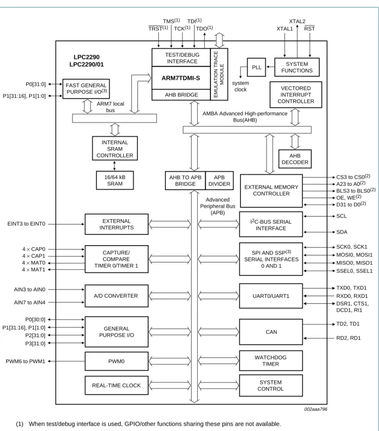
Block diagram
(1) When test/debug interface is used, GPIO/other functions sharing these pins are not available. (2) Pins shared with GPIO.
(3) Available in LPC2290/01 only. Fig 1. Block diagram
002aaa796 system clock SCL P0[30:0] P2[31:0] P1[31:16], P1[1:0] P3[31:0] SDA CS3 to CS0(2) A23 to A0(2) BLS3 to BLS0(2) OE, WE(2) D31 to D0(2) TRST(1) TMS(1) TCK(1) TDI(1) TDO(1) XTAL2 XTAL1 SCK0, SCK1 MOSI0, MOSI1 MISO0, MISO1 EINT3 to EINT0 4 × CAP0 4 × CAP1 4 × MAT1 4 × MAT0 AIN3 to AIN0 AIN7 to AIN4 PWM6 to PWM1 SSEL0, SSEL1 TD2, TD1 RD2, RD1 TXD0, TXD1 RXD0, RXD1 DSR1, CTS1, DCD1, RI1 AMBA Advanced High-performance
Bus(AHB) AHB BRIDGE EMULATION TRACE
MODULE TEST/DEBUG INTERFACE AHB DECODER AHB TO APB BRIDGE APB DIVIDER VECTORED INTERRUPT CONTROLLER SYSTEM FUNCTIONS PLL SPI AND SSP(3) SERIAL INTERFACES 0 AND 1 I2C-BUS SERIAL INTERFACE UART0/UART1 CAN WATCHDOG TIMER SYSTEM CONTROL EXTERNAL INTERRUPTS GENERAL PURPOSE I/O PWM0 CAPTURE/ COMPARE TIMER 0/TIMER 1 A/D CONVERTER ARM7TDMI-S LPC2290 LPC2290/01 INTERNAL SRAM CONTROLLER 16/64 kB SRAM ARM7 local bus Advanced Peripheral Bus (APB) REAL-TIME CLOCK RST EXTERNAL MEMORY CONTROLLER P0[31:0] P1[31:16], P1[1:0] FAST GENERAL PURPOSE I/O(3)
5.
Pinning information
5.1 Pinning
Fig 2. LQFP144 pinning LPC2290 108 37 72 14 4 10 9 73 1 36 002aaa7975.2 Pin description
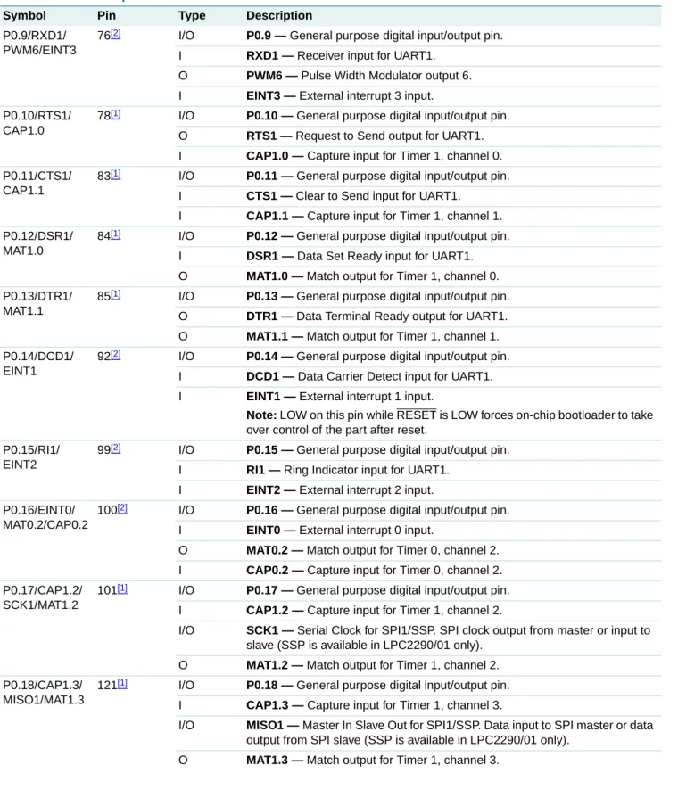
Table 3. Pin description
Symbol Pin Type Description
P0.0 to P0.31 I/O Port 0: Port 0 is a 32-bit bidirectional I/O port with individual direction controls
for each bit. The operation of port 0 pins depends upon the pin function selected via the Pin Connect Block.
Pins 26 and 31 of port 0 are not available. P0.0/TXD0/
PWM1
42[1] I/O P0.0 — General purpose digital input/output pin.
O TXD0 — Transmitter output for UART0.
O PWM1 — Pulse Width Modulator output 1.
P0.1/RXD0/ PWM3/EINT0
49[2] I/O P0.1 — General purpose digital input/output pin.
I RXD0 — Receiver input for UART0.
O PWM3 — Pulse Width Modulator output 3.
I EINT0 — External interrupt 0 input
P0.2/SCL/ CAP0.0
50[3] I/O P0.2 — General purpose digital input/output pin.
I/O SCL — I2C-bus clock input/output. Open-drain output (for I2C-bus
compliance).
I CAP0.0 — Capture input for Timer 0, channel 0.
P0.3/SDA/ MAT0.0/EINT1
58[3] I/O P0.3 — General purpose digital input/output pin.
I/O SDA — I2C-bus data input/output. Open-drain output (for I2C-bus
compliance).
O MAT0.0 — Match output for Timer 0, channel 0.
I EINT1 — External interrupt 1 input.
P0.4/SCK0/ CAP0.1
59[1] I/O P0.4 — General purpose digital input/output pin.
I/O SCK0 — Serial clock for SPI0. SPI clock output from master or input to slave.
I CAP0.1 — Capture input for Timer 0, channel 1.
P0.5/MISO0/ MAT0.1
61[1] I/O P0.5 — General purpose digital input/output pin.
I/O MISO0 — Master In Slave OUT for SPI0. Data input to SPI master or data
output from SPI slave.
O MAT0.1 — Match output for Timer 0, channel 1.
P0.6/MOSI0/ CAP0.2
68[1] I/O P0.6 — General purpose digital input/output pin.
I/O MOSI0 — Master Out Slave In for SPI0. Data output from SPI master or data
input to SPI slave.
I CAP0.2 — Capture input for Timer 0, channel 2.
P0.7/SSEL0/ PWM2/EINT2
69[2] I/O P0.7 — General purpose digital input/output pin.
I SSEL0 — Slave Select for SPI0. Selects the SPI interface as a slave.
O PWM2 — Pulse Width Modulator output 2.
I EINT2 — External interrupt 2 input.
P0.8/TXD1/ PWM4
75[1] I/O P0.8 — General purpose digital input/output pin.
O TXD1 — Transmitter output for UART1.
P0.9/RXD1/ PWM6/EINT3
76[2] I/O P0.9 — General purpose digital input/output pin.
I RXD1 — Receiver input for UART1.
O PWM6 — Pulse Width Modulator output 6.
I EINT3 — External interrupt 3 input.
P0.10/RTS1/ CAP1.0
78[1] I/O P0.10 — General purpose digital input/output pin.
O RTS1 — Request to Send output for UART1.
I CAP1.0 — Capture input for Timer 1, channel 0.
P0.11/CTS1/ CAP1.1
83[1] I/O P0.11 — General purpose digital input/output pin.
I CTS1 — Clear to Send input for UART1.
I CAP1.1 — Capture input for Timer 1, channel 1.
P0.12/DSR1/ MAT1.0
84[1] I/O P0.12 — General purpose digital input/output pin.
I DSR1 — Data Set Ready input for UART1.
O MAT1.0 — Match output for Timer 1, channel 0.
P0.13/DTR1/ MAT1.1
85[1] I/O P0.13 — General purpose digital input/output pin.
O DTR1 — Data Terminal Ready output for UART1.
O MAT1.1 — Match output for Timer 1, channel 1.
P0.14/DCD1/ EINT1
92[2] I/O P0.14 — General purpose digital input/output pin.
I DCD1 — Data Carrier Detect input for UART1.
I EINT1 — External interrupt 1 input.
Note: LOW on this pin while RESET is LOW forces on-chip bootloader to take
over control of the part after reset. P0.15/RI1/
EINT2
99[2] I/O P0.15 — General purpose digital input/output pin.
I RI1 — Ring Indicator input for UART1.
I EINT2 — External interrupt 2 input.
P0.16/EINT0/ MAT0.2/CAP0.2
100[2] I/O P0.16 — General purpose digital input/output pin.
I EINT0 — External interrupt 0 input.
O MAT0.2 — Match output for Timer 0, channel 2.
I CAP0.2 — Capture input for Timer 0, channel 2.
P0.17/CAP1.2/ SCK1/MAT1.2
101[1] I/O P0.17 — General purpose digital input/output pin.
I CAP1.2 — Capture input for Timer 1, channel 2.
I/O SCK1 — Serial Clock for SPI1/SSP. SPI clock output from master or input to
slave (SSP is available in LPC2290/01 only). O MAT1.2 — Match output for Timer 1, channel 2.
P0.18/CAP1.3/ MISO1/MAT1.3
121[1] I/O P0.18 — General purpose digital input/output pin.
I CAP1.3 — Capture input for Timer 1, channel 3.
I/O MISO1 — Master In Slave Out for SPI1/SSP. Data input to SPI master or data
output from SPI slave (SSP is available in LPC2290/01 only). O MAT1.3 — Match output for Timer 1, channel 3.
Table 3. Pin description …continued
P0.19/MAT1.2/ MOSI1/CAP1.2
122[1] I/O P0.19 — General purpose digital input/output pin.
O MAT1.2 — Match output for Timer 1, channel 2.
I/O MOSI1 — Master Out Slave In for SPI1/SSP. Data output from SPI master or
data input to SPI slave (SSP is available in LPC2290/01 only). I CAP1.2 — Capture input for Timer 1, channel 2.
P0.20/MAT1.3/ SSEL1/EINT3
123[2] I/O P0.20 — General purpose digital input/output pin.
O MAT1.3 — Match output for Timer 1, channel 3.
I SSEL1 — Slave Select for SPI1/SSP. Selects the SPI interface as a slave
(SSP is available in LPC2290/01 only). I EINT3 — External interrupt 3 input.
P0.21/PWM5/ CAP1.3
4[1] I/O P0.21 — General purpose digital input/output pin.
O PWM5 — Pulse Width Modulator output 5.
I CAP1.3 — Capture input for Timer 1, channel 3.
P0.22/CAP0.0/ MAT0.0
5[1] I/O P0.22 — General purpose digital input/output pin.
I CAP0.0 — Capture input for Timer 0, channel 0.
O MAT0.0 — Match output for Timer 0, channel 0.
P0.23/RD2 6[1] I/O P0.23 — General purpose digital input/output pin.
I RD2 — CAN2 receiver input.
P0.24/TD2 8[1] I/O P0.24 — General purpose digital input/output pin.
O TD2 — CAN2 transmitter output.
P0.25 21[1] I/O P0.25 — General purpose digital input/output pin.
I RD1 — CAN1 receiver input.
P0.27/AIN0/ CAP0.1/MAT0.1
23[4] I/O P0.27 — General purpose digital input/output pin.
I AIN0 — ADC, input 0. This analog input is always connected to its pin.
I CAP0.1 — Capture input for Timer 0, channel 1.
O MAT0.1 — Match output for Timer 0, channel 1.
P0.28/AIN1/ CAP0.2/MAT0.2
25[4] I/O P0.28 — General purpose digital input/output pin.
I AIN1 — ADC, input 1. This analog input is always connected to its pin.
I CAP0.2 — Capture input for Timer 0, channel 2.
O MAT0.2 — Match output for Timer 0, channel 2.
P0.29/AIN2/ CAP0.3/MAT0.3
32[4] I/O P0.29 — General purpose digital input/output pin.
I AIN2 — ADC, input 2. This analog input is always connected to its pin.
I CAP0.3 — Capture input for Timer 0, Channel 3.
O MAT0.3 — Match output for Timer 0, channel 3.
P0.30/AIN3/ EINT3/CAP0.0
33[4] I/O P0.30 — General purpose digital input/output pin.
I AIN3 — ADC, input 3. This analog input is always connected to its pin.
I EINT3 — External interrupt 3 input.
I CAP0.0 — Capture input for Timer 0, channel 0.
P1.0 to P1.31 I/O Port 1: Port 1 is a 32-bit bidirectional I/O port with individual direction controls
for each bit. The operation of port 1 pins depends upon the pin function selected via the Pin Connect Block.
Pins 2 through 15 of port 1 are not available.
Table 3. Pin description …continued
P1.0/CS0 91[5] I/O P1.0 — General purpose digital input/output pin.
O CS0 — LOW-active Chip Select 0 signal.
(Bank 0 addresses range 0x8000 0000 to 0x80FF FFFF) P1.1/OE 90[5] I/O P1.1 — General purpose digital input/output pin.
O OE — LOW-active Output Enable signal.
P1.16/ TRACEPKT0
34[5] I/O P1.16 — General purpose digital input/output pin.
O TRACEPKT0 — Trace Packet, bit 0. Standard I/O port with internal pull-up.
P1.17/ TRACEPKT1
24[5] I/O P1.17 — General purpose digital input/output pin.
O TRACEPKT1 — Trace Packet, bit 1. Standard I/O port with internal pull-up.
P1.18/ TRACEPKT2
15[5] I/O P1.18 — General purpose digital input/output pin.
O TRACEPKT2 — Trace Packet, bit 2. Standard I/O port with internal pull-up.
P1.19/ TRACEPKT3
7[5] I/O P1.19 — General purpose digital input/output pin.
O TRACEPKT3 — Trace Packet, bit 3. Standard I/O port with internal pull-up.
P1.20/ TRACESYNC
102[5] I/O P1.20 — General purpose digital input/output pin.
O TRACESYNC — Trace Synchronization. Standard I/O port with internal
pull-up.
Note: LOW on this pin while RESET is LOW, enables pins P1[25:16] to
operate as Trace port after reset. P1.21/
PIPESTAT0
95[5] I/O P1.21 — General purpose digital input/output pin.
O PIPESTAT0 — Pipeline Status, bit 0. Standard I/O port with internal pull-up.
P1.22/ PIPESTAT1
86[5] I/O P1.22 — General purpose digital input/output pin.
O PIPESTAT1 — Pipeline Status, bit 1. Standard I/O port with internal pull-up.
P1.23/ PIPESTAT2
82[5] I/O P1.23 — General purpose digital input/output pin.
O PIPESTAT2 — Pipeline Status, bit 2. Standard I/O port with internal pull-up.
P1.24/ TRACECLK
70[5] I/O P1.24 — General purpose digital input/output pin.
O TRACECLK — Trace Clock. Standard I/O port with internal pull-up.
P1.25/EXTIN0 60[5] I/O P1.25 — General purpose digital input/output pin.
I EXTIN0 — External Trigger Input. Standard I/O with internal pull-up.
P1.26/RTCK 52[5] I/O P1.26 — General purpose digital input/output pin.
I/O RTCK — Returned Test Clock output. Extra signal added to the JTAG port.
Assists debugger synchronization when processor frequency varies. Bidirectional pin with internal pull-up.
Note: LOW on this pin while RESET is LOW, enables pins P1[31:26] to
operate as Debug port after reset.
P1.27/TDO 144[5] I/O P1.27 — General purpose digital input/output pin.
O TDO — Test Data out for JTAG interface.
P1.28/TDI 140[5] I/O P1.28 — General purpose digital input/output pin.
I TDI — Test Data in for JTAG interface.
P1.29/TCK 126[5] I/O P1.29 — General purpose digital input/output pin.
I TCK — Test Clock for JTAG interface.
P1.30/TMS 113[5] I/O P1.30 — General purpose digital input/output pin.
I TMS — Test Mode Select for JTAG interface.
Table 3. Pin description …continued
P1.31/TRST 43[5] I/O P1.31 — General purpose digital input/output pin.
I TRST — Test Reset for JTAG interface.
P2.0 to P2.31 I/O Port 2 — Port 2 is a 32-bit bidirectional I/O port with individual direction
controls for each bit. The operation of port 2 pins depends upon the pin function selected via the Pin Connect Block.
P2.0/D0 98[5] I/O P2.0 — General purpose digital input/output pin.
I/O D0 — External memory data line 0.
P2.1/D1 105[5] I/O P2.1 — General purpose digital input/output pin.
I/O D1 — External memory data line 1.
P2.2/D2 106[5] I/O P2.2 — General purpose digital input/output pin.
I/O D2 — External memory data line 2.
P2.3/D3 108[5] I/O P2.3 — General purpose digital input/output pin.
I/O D3 — External memory data line 3.
P2.4/D4 109[5] I/O P2.4 — General purpose digital input/output pin.
I/O D4 — External memory data line 4.
P2.5/D5 114[5] I/O P2.5 — General purpose digital input/output pin.
I/O D5 — External memory data line 5.
P2.6/D6 115[5] I/O P2.6 — General purpose digital input/output pin.
I/O D6 — External memory data line 6.
P2.7/D7 116[5] I/O P2.7 — General purpose digital input/output pin.
I/O D7 — External memory data line 7.
P2.8/D8 117[5] I/O P2.8 — General purpose digital input/output pin.
I/O D8 — External memory data line 8.
P2.9/D9 118[5] I/O P2.9 — General purpose digital input/output pin.
I/O D9 — External memory data line 9.
P2.10/D10 120[5] I/O P2.10 — General purpose digital input/output pin.
I/O D10 — External memory data line 10.
P2.11/D11 124[5] I/O P2.11 — General purpose digital input/output pin.
I/O D11 — External memory data line 11.
P2.12/D12 125[5] I/O P2.12 — General purpose digital input/output pin.
I/O D12 — External memory data line 12.
P2.13/D13 127[5] I/O P2.13 — General purpose digital input/output pin.
I/O D13 — External memory data line 13.
P2.14/D14 129[5] I/O P2.14 — General purpose digital input/output pin.
I/O D14 — External memory data line 14.
P2.15/D15 130[5] I/O P2.15 — General purpose digital input/output pin.
I/O D15 — External memory data line 15.
P2.16/D16 131[5] I/O P2.16 — General purpose digital input/output pin.
I/O D16 — External memory data line 16.
P2.17/D17 132[5] I/O P2.17 — General purpose digital input/output pin.
I/O D17 — External memory data line 17.
Table 3. Pin description …continued
P2.18/D18 133[5] I/O P2.18 — General purpose digital input/output pin.
I/O D18 — External memory data line 18.
P2.19/D19 134[5] I/O P2.19 — General purpose digital input/output pin.
I/O D19 — External memory data line 19.
P2.20/D20 136[5] I/O P2.20 — General purpose digital input/output pin.
I/O D20 — External memory data line 20.
P2.21/D21 137[5] I/O P2.21 — General purpose digital input/output pin.
I/O D21 — External memory data line 21.
P2.22/D22 1[5] I/O P2.22 — General purpose digital input/output pin.
I/O D22 — External memory data line 22.
P2.23/D23 10[5] I/O P2.23 — General purpose digital input/output pin.
I/O D23 — External memory data line 23.
P2.24/D24 11[5] I/O P2.24 — General purpose digital input/output pin.
I/O D24 — External memory data line 24.
P2.25/D25 12[5] I/O P2.25 — General purpose digital input/output pin.
I/O D25 — External memory data line 25.
P2.26/D26/ BOOT0
13[5] I/O P2.26 — General purpose digital input/output pin.
I/O D26 — External memory data line 26.
I BOOT0 — While RESET is low, together with BOOT1 controls booting and
internal operation. Internal pull-up ensures high state if pin is left unconnected.
P2.27/D27/ BOOT1
16[5] I/O P2.27 — General purpose digital input/output pin.
I/O D27 — External memory data line 27.
I BOOT1 — While RESET is low, together with BOOT0 controls booting and
internal operation. Internal pull-up ensures high state if pin is left unconnected.
BOOT1:0 = 00 selects 8-bit memory on CS0 for boot. BOOT1:0 = 01 selects 16-bit memory on CS0 for boot. BOOT1:0 = 10 selects 32-bit memory on CS0 for boot. BOOT1:0 = 11 selects internal flash memory.
P2.28/D28 17[5] I/O P2.28 — General purpose digital input/output pin.
I/O D28 — External memory data line 28.
P2.29/D29 18[5] I/O P2.29 — General purpose digital input/output pin.
I/O D29 — External memory data line 29.
P2.30/D30/ AIN4
19[2] I/O P2.30 — General purpose digital input/output pin.
I/O D30 — External memory data line 30.
I AIN4 — ADC, input 4. This analog input is always connected to its pin.
P2.31/D31/ AIN5
20[2] I/O P2.31 — General purpose digital input/output pin.
I/O D31 — External memory data line 31.
I AIN5 — ADC, input 5. This analog input is always connected to its pin.
P3.0 to P3.31 I/O Port 3 — Port 3 is a 32-bit bidirectional I/O port with individual direction
controls for each bit. The operation of port 3 pins depends upon the pin function selected via the Pin Connect Block.
Table 3. Pin description …continued
P3.0/A0 89[5] I/O P3.0 — General purpose digital input/output pin.
O A0 — External memory address line 0.
P3.1/A1 88[5] I/O P3.1 — General purpose digital input/output pin.
O A1 — External memory address line 1.
P3.2/A2 87[5] I/O P3.2 — General purpose digital input/output pin.
O A2 — External memory address line 2.
P3.3/A3 81[5] I/O P3.3 — General purpose digital input/output pin.
O A3 — External memory address line 3.
P3.4/A4 80[5] I/O P3.4 — General purpose digital input/output pin.
O A4 — External memory address line 4.
P3.5/A5 74[5] I/O P3.5 — General purpose digital input/output pin.
O A5 — External memory address line 5.
P3.6/A6 73[5] I/O P3.6 — General purpose digital input/output pin.
O A6 — External memory address line 6.
P3.7/A7 72[5] I/O P3.7 — General purpose digital input/output pin.
O A7 — External memory address line 7.
P3.8/A8 71[5] I/O P3.8 — General purpose digital input/output pin.
O A8 — External memory address line 8.
P3.9/A9 66[5] I/O P3.9 — General purpose digital input/output pin.
O A9 — External memory address line 9.
P3.10/A10 65[5] I/O P3.10 — General purpose digital input/output pin.
O A10 — External memory address line 10.
P3.11/A11 64[5] I/O P3.11 — General purpose digital input/output pin.
O A11 — External memory address line 11.
P3.12/A12 63[5] I/O P3.12 — General purpose digital input/output pin.
O A12 — External memory address line 12.
P3.13/A13 62[5] I/O P3.13 — General purpose digital input/output pin.
O A13 — External memory address line 13.
P3.14/A14 56[5] I/O P3.14 — General purpose digital input/output pin.
O A14 — External memory address line 14.
P3.15/A15 55[5] I/O P3.15 — General purpose digital input/output pin.
O A15 — External memory address line 15.
P3.16/A16 53[5] I/O P3.16 — General purpose digital input/output pin.
O A16 — External memory address line 16.
P3.17/A17 48[5] I/O P3.17 — General purpose digital input/output pin.
O A17 — External memory address line 17.
P3.18/A18 47[5] I/O P3.18 — General purpose digital input/output pin.
O A18 — External memory address line 18.
P3.19/A19 46[5] I/O P3.19 — General purpose digital input/output pin.
O A19 — External memory address line 19.
Table 3. Pin description …continued
P3.20/A20 45[5] I/O P3.20 — General purpose digital input/output pin.
O A20 — External memory address line 20.
P3.21/A21 44[5] I/O P3.21 — General purpose digital input/output pin.
O A21 — External memory address line 21.
P3.22/A22 41[5] I/O P3.22 — General purpose digital input/output pin.
O A22 — External memory address line 22.
P3.23/A23/ XCLK
40[5] I/O P3.23 — General purpose digital input/output pin.
I/O A23 — External memory address line 23.
O XCLK — Clock output.
P3.24/CS3 36[5] I/O P3.24 — General purpose digital input/output pin.
O CS3 — LOW-active Chip Select 3 signal.
(Bank 3 addresses range 0x8300 0000 to 0x83FF FFFF) P3.25/CS2 35[5] I/O P3.25 — General purpose digital input/output pin.
O CS2 — LOW-active Chip Select 2 signal.
(Bank 2 addresses range 0x8200 0000 to 0x82FF FFFF) P3.26/CS1 30[5] I/O P3.26 — General purpose digital input/output pin.
O CS1 — LOW-active Chip Select 1 signal.
(Bank 1 addresses range 0x8100 0000 to 0x81FF FFFF) P3.27/WE 29[5] I/O P3.27 — General purpose digital input/output pin.
O WE — LOW-active Write enable signal.
P3.28/BLS3/ AIN7
28[2] I/O P3.28 — General purpose digital input/output pin.
O BLS3 — LOW-active Byte Lane Select signal (Bank 3).
I AIN7 — ADC, input 7. This analog input is always connected to its pin.
P3.29/BLS2/ AIN6
27[4] I/O P3.29 — General purpose digital input/output pin.
O BLS2 — LOW-active Byte Lane Select signal (Bank 2).
I AIN6 — ADC, input 6. This analog input is always connected to its pin.
P3.30/BLS1 97[4] I/O P3.30 — General purpose digital input/output pin.
O BLS1 — LOW-active Byte Lane Select signal (Bank 1).
P3.31/BLS0 96[4] I/O P3.31 — General purpose digital input/output pin.
O BLS0 — LOW-active Byte Lane Select signal (Bank 0).
TD1 22[5] O TD1: CAN1 transmitter output.
RESET 135[6] I External Reset input: A LOW on this pin resets the device, causing I/O ports
and peripherals to take on their default states, and processor execution to begin at address 0. TTL with hysteresis, 5 V tolerant.
XTAL1 142[7] I Input to the oscillator circuit and internal clock generator circuits.
XTAL2 141[7] O Output from the oscillator amplifier.
VSS 3, 9, 26, 38,
54, 67, 79, 93, 103, 107, 111, 128
I Ground: 0 V reference.
VSSA 139 I Analog ground: 0 V reference. This should nominally be the same voltage
as VSS, but should be isolated to minimize noise and error.
Table 3. Pin description …continued
[1] 5 V tolerant pad providing digital I/O functions with TTL levels and hysteresis and 10 ns slew rate control.
[2] 5 V tolerant pad providing digital I/O functions with TTL levels and hysteresis and 10 ns slew rate control. If configured for an input function, this pad utilizes built-in glitch filter that blocks pulses shorter than 3 ns.
[3] Open-drain 5 V tolerant digital I/O I2C-bus 400 kHz specification compatible pad. It requires external pull-up to provide an output functionality.
[4] 5 V tolerant pad providing digital I/O (with TTL levels and hysteresis and 10 ns slew rate control) and analog input function. If configured for a digital input function, this pad utilizes built-in glitch filter that blocks pulses shorter than 3 ns. When configured as an ADC input, digital section of the pad is disabled.
[5] 5 V tolerant pad with built-in pull-up resistor providing digital I/O functions with TTL levels and hysteresis and 10 ns slew rate control. The pull-up resistor’s value ranges from 60 kΩ to 300 kΩ.
[6] 5 V tolerant pad providing digital input (with TTL levels and hysteresis) function only. [7] Pad provides special analog functionality.
VSSA(PLL) 138 I PLL analog ground: 0 V reference. This should nominally be the same
voltage as VSS, but should be isolated to minimize noise and error.
VDD(1V8) 37, 110 I 1.8 V core power supply: This is the power supply voltage for internal
circuitry.
VDDA(1V8) 143 I Analog 1.8 V core power supply: This is the power supply voltage for
internal circuitry. This should be nominally the same voltage as VDD(1V8) but
should be isolated to minimize noise and error. VDD(3V3) 2, 31, 39, 51,
57, 77, 94, 104, 112, 119
I 3.3 V pad power supply: This is the power supply voltage for the I/O ports.
VDDA(3V3) 14 I Analog 3.3 V pad power supply: This should be nominally the same voltage
as VDD(3V3) but should be isolated to minimize noise and error.
Table 3. Pin description …continued
6.
Functional description
6.1 Architectural overview
The ARM7TDMI-S is a general purpose 32-bit microprocessor, which offers high performance and very low power consumption. The ARM architecture is based on RISC principles, and the instruction set and related decode mechanism are much simpler than those of microprogrammed CISC. This simplicity results in a high instruction throughput and impressive real-time interrupt response from a small and cost-effective processor core.
Pipeline techniques are employed so that all parts of the processing and memory systems can operate continuously. Typically, while one instruction is being executed, its successor is being decoded, and a third instruction is being fetched from memory.
The ARM7TDMI-S processor also employs a unique architectural strategy known as Thumb, which makes it ideally suited to high-volume applications with memory restrictions, or applications where code density is an issue.
The key idea behind Thumb is that of a super-reduced instruction set. Essentially, the ARM7TDMI-S processor has two instruction sets:
•
The standard 32-bit ARM set.•
A 16-bit Thumb set.The Thumb set’s 16-bit instruction length allows it to approach twice the density of standard ARM code while retaining most of the ARM’s performance advantage over a traditional 16-bit processor using 16-bit registers. This is possible because Thumb code operates on the same 32-bit register set as ARM code.
Thumb code is able to provide up to 65 % of the code size of ARM, and 160 % of the performance of an equivalent ARM processor connected to a 16-bit memory system.
6.2 On-chip SRAM
On-chip SRAM may be used for code and/or data storage. The SRAM may be accessed as 8-bit, 16-bit, and 32-bit. The LPC2290 provides 16 kB of SRAM and the LPC2290/01 provides 64 kB of SRAM.
6.3 Memory map
The LPC2290 memory maps incorporate several distinct regions, as shown inFigure 3. In addition, the CPU interrupt vectors may be re-mapped to allow them to reside in either on-chip bootloader, external memory BANK0 or on-chip static RAM. This is described in Section 6.18 “System control”.
6.4 Interrupt controller
The Vectored Interrupt Controller (VIC) accepts all of the interrupt request inputs and categorizes them as Fast Interrupt Request (FIQ), vectored Interrupt Request (IRQ), and non-vectored IRQ as defined by programmable settings. The programmable assignment scheme means that priorities of interrupts from the various peripherals can be dynamically assigned and adjusted.
FIQ has the highest priority. If more than one request is assigned to FIQ, the VIC combines the requests to produce the FIQ signal to the ARM processor. The fastest possible FIQ latency is achieved when only one request is classified as FIQ, because then the FIQ service routine can simply start dealing with that device. But if more than one request is assigned to the FIQ class, the FIQ service routine can read a word from the VIC that identifies which FIQ source(s) is (are) requesting an interrupt.
Fig 3. LPC2290 and LPC2290/01 memory map
AHB PERIPHERALS VPB PERIPHERALS
RESERVED ADDRESS SPACE
RESERVED ADDRESS SPACE
16 KBYTE ON-CHIP STATIC RAM 64 KBYTE ON-CHIP STATIC RAM (/01 ONLY)
RESERVED ADDRESS SPACE
0xFFFF FFFF 0xF000 0000 0xEFFF FFFF 0xE000 0000 0xDFFF FFFF 0x4000 4000 0x4000 3FFF 0x4001 0000 0x4000 FFFF 0x4000 0000 0x3FFF FFFF 4.0 GB 3.75 GB 3.5 GB 3.0 GB 2.0 GB 1.0 GB 0.0 GB 0x0000 0000 002aaa798 0x8400 0000 0x7FFF FFFF EXTERNAL MEMORY BANK3
0x83FF FFFF 0x8300 0000 EXTERNAL MEMORY BANK2
0x82FF FFFF 0x8200 0000 EXTERNAL MEMORY BANK1
0x81FF FFFF 0x8100 0000 EXTERNAL MEMORY BANK0
0x80FF FFFF 0x8000 0000 BOOT BLOCK (RE-MAPPED FROM
ON-CHIP ROM MEMORY 0x7FFF E000 0x7FFF DFFF
Vectored IRQs have the middle priority. Sixteen of the interrupt requests can be assigned to this category. Any of the interrupt requests can be assigned to any of the 16 vectored IRQ slots, among which slot 0 has the highest priority and slot 15 has the lowest. Non-vectored IRQs have the lowest priority.
The VIC combines the requests from all the vectored and non-vectored IRQs to produce the IRQ signal to the ARM processor. The IRQ service routine can start by reading a register from the VIC and jumping there. If any of the vectored IRQs are requesting, the VIC provides the address of the highest-priority requesting IRQs service routine,
otherwise it provides the address of a default routine that is shared by all the non-vectored IRQs. The default routine can read another VIC register to see what IRQs are active.
6.4.1 Interrupt sources
Table 4lists the interrupt sources for each peripheral function. Each peripheral device has one interrupt line connected to the VIC, but may have several internal interrupt flags. Individual interrupt flags may also represent more than one interrupt source.
Table 4. Interrupt sources
Block Flag(s) VIC channel #
WDT Watchdog Interrupt (WDINT) 0 - Reserved for software interrupts only 1 ARM Core EmbeddedICE, DbgCommRx 2 ARM Core EmbeddedICE, DbgCommTx 3 Timer 0 Match 0 to 3 (MR0, MR1, MR2, MR3) Capture 0 to 3 (CR0, CR1, CR2, CR3) 4 Timer 1 Match 0 to 3 (MR0, MR1, MR2, MR3) Capture 0 to 3 (CR0, CR1, CR2, CR3) 5 UART0 RX Line Status (RLS)
Transmit Holding Register Empty (THRE) RX Data Available (RDA)
Character Time-out Indicator (CTI)
6
Auto-Baud Time-Out (ABTO) (available in LPC2290/01 only) End of Auto-Baud (ABEO)
UART1 RX Line Status (RLS)
Transmit Holding Register empty (THRE) RX Data Available (RDA)
Character Time-out Indicator (CTI) Modem Status Interrupt (MSI)
7
Auto-Baud Time-Out (ABTO) (available in LPC2290/01 only) End of Auto-Baud (ABEO)
PWM0 Match 0 to 6 (MR0, MR1, MR2, MR3, MR4, MR5, MR6) 8 I2C-bus SI (state change) 9
6.5 Pin connect block
The pin connect block allows selected pins of the microcontroller to have more than one function. Configuration registers control the multiplexers to allow connection between the pin and the on-chip peripherals. Peripherals should be connected to the appropriate pins prior to being activated, and prior to any related interrupt(s) being enabled. Activity of any enabled peripheral function that is not mapped to a related pin should be considered undefined.
6.6 External memory controller
The external Static Memory Controller is a module which provides an interface between the system bus and external (off-chip) memory devices. It provides support for up to four independently configurable memory banks (16 MB each with byte lane enable control) simultaneously. Each memory bank is capable of supporting SRAM, ROM, flash EPROM, burst ROM memory, or some external I/O devices.
Each memory bank may be 8-bit, 16-bit, or 32-bit wide.
6.7 General purpose parallel I/O and Fast I/O
Device pins that are not connected to a specific peripheral function are controlled by the GPIO registers. Pins may be dynamically configured as inputs or outputs. Separate registers allow setting or clearing any number of outputs simultaneously. The value of the output register may be read back, as well as the current state of the port pins.
6.7.1 Features
•
Direction control of individual bits.•
Separate control of output set and clear.SPI1/SSP Source: SPI1 SPI Interrupt Flag (SPIF), Mode Fault (MODF) 11
Source: SSP (available in LPC2290/01 only)
TX FIFO at least half empty (TXRIS) RX FIFO at least half full (RXRIS) Receive Timeout condition (RTRIS) Receive Overrun (RORRIS)
PLL PLL Lock (PLOCK) 12 RTC RTCCIF (Counter Increment), RTCALF (Alarm) 13 System Control External Interrupt 0 (EINT0) 14 External Interrupt 1 (EINT1) 15 External Interrupt 2 (EINT2) 16 External Interrupt 3 (EINT3) 17
A/D ADC 18
CAN 1 ORed CAN Acceptance Filter 19 CAN1 (TX int, RX int) 20, 21 CAN2 (TX int, RX int) 22, 23
Table 4. Interrupt sources …continued
•
All I/O default to inputs after reset.6.7.2 Fast I/O features available in LPC2290/01 only
•
Fast I/O registers are located on the ARM local bus for the fastest possible I/O timing.•
All GPIO registers are byte addressable.•
Entire port value can be written in one instruction.•
Mask registers allow single instruction to set or clear any number of bits in one port.6.8 10-bit ADC
The LPC2290 each contain a single 10-bit successive approximation ADC with eight multiplexed channels.
6.8.1 Features
•
Measurement range of 0 V to 3.3 V.•
Capable of performing more than 400000 10-bit samples per second.•
Burst conversion mode for single or multiple inputs.•
Optional conversion on transition on input pin or Timer Match signal.6.8.2 ADC features available in LPC2290/01 only
•
Every analog input has a dedicated result register to reduce interrupt overhead.•
Every analog input can generate an interrupt once the conversion is completed.6.9 CAN controllers and acceptance filter
The LPC2290 contains two CAN controllers. The CAN is a serial communications protocol which efficiently supports distributed real-time control with a very high level of security. Its domain of application ranges from high-speed networks to low cost multiplex wiring.
6.9.1 Features
•
Data rates up to 1 Mbit/s on each bus.•
32-bit register and RAM access.•
Compatible with CAN specification 2.0B, ISO 11898-1.•
Global Acceptance Filter recognizes 11-bit and 29-bit RX identifiers for all CAN buses.•
Acceptance Filter can provide FullCAN-style automatic reception for selectedStandard identifiers.
•
Full CAN messages can generate interrupts.6.10 UARTs
The LPC2290 contains two UARTs. In addition to standard transmit and receive data lines, UART1 also provides a full modem control handshake interface.
6.10.1 Features
•
Register locations conform to 16C550 industry standard.•
Receiver FIFO trigger points at 1 B, 4 B, 8 B, and 14 B.•
Built-in baud rate generator.•
Standard modem interface signals included on UART1.6.10.2 UART features available in LPC2290/01 only
•
The transmission FIFO control enables implementation of software (XON/XOFF) flow control on both UARTs and hardware (CTS/RTS) flow control on UART1 only.•
Fractional baud rate generator enables standard baud rates such as 115200 to beachieved with any crystal frequency above 2 MHz.
•
Auto-bauding.•
Auto-CTS/RTS flow-control fully implemented in hardware.6.11 I
2C-bus serial I/O controller
The I2C-bus is bidirectional, for inter-IC control using only two wires: a serial clock line (SCL), and a serial data line (SDA). Each device is recognized by a unique address and can operate as either a receiver-only device (e.g., an LCD driver or a transmitter with the capability to both receive and send information (such as memory). Transmitters and/or receivers can operate in either master or slave mode, depending on whether the chip has to initiate a data transfer or is only addressed. The I2C-bus is a multi-master bus, it can be controlled by more than one bus master connected to it.
The I2C-bus implemented in LPC2290 supports bit rate up to 400 kbit/s (Fast I2C-bus).
6.11.1 Features
•
Compliant with standard I2C-bus interface.•
Easy to configure as master, slave, or master/slave.•
Programmable clocks allow versatile rate control.•
Bidirectional data transfer between masters and slaves.•
Multi-master bus (no central master).•
Arbitration between simultaneously transmitting masters without corruption of serial data on the bus.•
Serial clock synchronization allows devices with different bit rates to communicate via one serial bus.•
Serial clock synchronization can be used as a handshake mechanism to suspend and resume serial transfer.•
The I2C-bus may be used for test and diagnostic purposes.6.12 SPI serial I/O controller
The LPC2290 contains two SPIs. The SPI is a full duplex serial interface, designed to be able to handle multiple masters and slaves connected to a given bus. Only a single master and a single slave can communicate on the interface during a given data transfer. During a data transfer the master always sends a byte of data to the slave, and the slave always sends a byte of data to the master.
6.12.1 Features
•
Compliant with SPI specification.•
Synchronous, serial, full duplex, communication.•
Combined SPI master and slave.•
Maximum data bit rate of one eighth of the input clock rate.6.13 SSP serial I/O controller (available in LPC2290/01 only)
The LPC2290/01 contains one Serial Synchronous Port controller (SSP). The SSP controller is capable of operation on a SPI, 4-wire SSI, or Microwire bus. It can interact with multiple masters and slaves on the bus. However, only a single master and a single slave can communicate on the bus during a given data transfer. The SSP supports full duplex transfers, with frames of 4 bits to 16 bits of data flowing from the master to the slave and from the slave to the master. Often only one of these data flows carries meaningful data.
The SSP and SPI1 share the same pins on LPC2290/01. After a reset, SPI1 is enabled and SSP is disabled.
6.13.1 Features
•
Synchronous Serial Communication.•
8-frame FIFOs for both transmit and receive.•
Compatible with Motorola SPI, 4-wire TI SSI and National Semiconductor Microwire buses.•
Master or slave operation.•
Four bits to 16 bits per SPI frame.6.14 General purpose timers
The TIMER0 and TIMER1 are designed to count cycles of the peripheral clock (PCLK) and optionally generate interrupts or perform other actions at specified timer values, based on four match registers. It also includes four capture inputs to trap the timer value when an input signal transitions, optionally generating an interrupt. Multiple pins can be selected to perform a single capture or match function, providing an application with ‘or’ and ‘and’, as well as ‘broadcast’ functions among them.
6.14.1 Features
•
A 32-bit Timer/Counter with a programmable 32-bit prescaler.•
Four 32-bit capture channels per timer that can take a snapshot of the timer value when an input signal transitions. A capture event may also optionally generate an interrupt.•
Four 32-bit match registers that allow:– Continuous operation with optional interrupt generation on match. – Stop timer on match with optional interrupt generation.
•
Four external outputs per timer corresponding to match registers, with the following capabilities:– Set LOW on match. – Set HIGH on match. – Toggle on match. – Do nothing on match.
6.14.2 Timer features available in LPC2290/01 only
•
Timers can count cycles of the externally supplied clock providing external event counting functionality6.15 Watchdog timer
The purpose of the watchdog is to reset the microcontroller within a reasonable amount of time if it enters an erroneous state. When enabled, the watchdog will generate a system reset if the user program fails to ‘feed’ (or reload) the watchdog within a predetermined amount of time.
6.15.1 Features
•
Internally resets chip if not periodically reloaded.•
Debug mode.•
Enabled by software but requires a hardware reset or a watchdog reset/interrupt to be disabled.•
Incorrect/incomplete feed sequence causes reset/interrupt if enabled.•
Flag to indicate watchdog reset.•
Programmable 32-bit timer with internal pre-scaler.•
Selectable time period from (Tcy(PCLK)×256×4) to (Tcy(PCLK)×232×4) in multiples of Tcy(PCLK)× 4.6.16 Real-time clock
The Real-Time Clock (RTC) is designed to provide a set of counters to measure time when normal or idle operating mode is selected. The RTC has been designed to use little power, making it suitable for battery powered systems where the CPU is not running continuously (Idle mode).
6.16.1 Features
•
Measures the passage of time to maintain a calendar and clock.•
Ultra-low power design to support battery powered systems.•
Provides Seconds, Minutes, Hours, Day of Month, Month, Year, Day of Week, and Day of Year.•
Programmable Reference Clock Divider allows adjustment of the RTC to match various crystal frequencies.6.17 Pulse width modulator
The PWM is based on the standard Timer block and inherits all of its features, although only the PWM function is pinned out on the LPC2290. The Timer is designed to count cycles of the peripheral clock (PCLK) and optionally generate interrupts or perform other actions when specified timer values occur, based on seven match registers. The PWM function is also based on match register events.
The ability to separately control rising and falling edge locations allows the PWM to be used for more applications. For instance, multi-phase motor control typically requires three non-overlapping PWM outputs with individual control of all three pulse widths and
positions.
Two match registers can be used to provide a single edge controlled PWM output. One match register (MR0) controls the PWM cycle rate, by resetting the count upon match. The other match register controls the PWM edge position. Additional single edge
controlled PWM outputs require only one match register each, since the repetition rate is the same for all PWM outputs. Multiple single edge controlled PWM outputs will all have a rising edge at the beginning of each PWM cycle, when an MR0 match occurs.
Three match registers can be used to provide a PWM output with both edges controlled. Again, the MR0 match register controls the PWM cycle rate. The other match registers control the two PWM edge positions. Additional double edge controlled PWM outputs require only two match registers each, since the repetition rate is the same for all PWM outputs.
With double edge controlled PWM outputs, specific match registers control the rising and falling edge of the output. This allows both positive going PWM pulses (when the rising edge occurs prior to the falling edge), and negative going PWM pulses (when the falling edge occurs prior to the rising edge).
6.17.1 Features
•
Seven match registers allow up to six single edge controlled or three double edge controlled PWM outputs, or a mix of both types.•
The match registers also allow:– Continuous operation with optional interrupt generation on match. – Stop timer on match with optional interrupt generation.
– Reset timer on match with optional interrupt generation.
•
Supports single edge controlled and/or double edge controlled PWM outputs. Single edge controlled PWM outputs all go HIGH at the beginning of each cycle unless the output is a constant LOW. Double edge controlled PWM outputs can have either edge occur at any position within a cycle. This allows for both positive going and negative going pulses.•
Pulse period and width can be any number of timer counts. This allows complete flexibility in the trade-off between resolution and repetition rate. All PWM outputs will occur at the same repetition rate.•
Double edge controlled PWM outputs can be programmed to be either positive going or negative going pulses.•
Match register updates are synchronized with pulse outputs to prevent generation of erroneous pulses. Software must ‘release’ new match values before they can become effective.•
May be used as a standard timer if the PWM mode is not enabled.•
A 32-bit Timer/Counter with a programmable 32-bit prescaler.6.18 System control
6.18.1 Crystal oscillator
The oscillator supports crystals in the range of 1 MHz to 30 MHz. The oscillator output frequency is called foscand the ARM processor clock frequency is referred to as CCLK for purposes of rate equations, etc. fosc and CCLK are the same value unless the PLL is running and connected. Refer toSection 6.18.2 “PLL” for additional information.
6.18.2 PLL
The PLL accepts an input clock frequency in the range of 10 MHz to 25 MHz. The input frequency is multiplied up into the range of 10 MHz to 60 MHz with a Current Controlled Oscillator (CCO). The multiplier can be an integer value from 1 to 32 (in practice, the multiplier value cannot be higher than 6 on this family of microcontrollers due to the upper frequency limit of the CPU). The CCO operates in the range of 156 MHz to 320 MHz, so there is an additional divider in the loop to keep the CCO within its frequency range while the PLL is providing the desired output frequency. The output divider may be set to divide by 2, 4, 8, or 16 to produce the output clock. Since the minimum output divider value is 2, it is insured that the PLL output has a 50 % duty cycle.The PLL is turned off and bypassed following a chip reset and may be enabled by software. The program must configure and activate the PLL, wait for the PLL to Lock, then connect to the PLL as a clock source. The PLL settling time is 100µs.
6.18.3 Reset and wake-up timer
Reset has two sources on the LPC2290: the RESET pin and watchdog reset. The RESET pin is a Schmitt trigger input pin with an additional glitch filter. Assertion of chip reset by any source starts the Wake-up Timer (see Wake-up Timer description below), causing the internal chip reset to remain asserted until the external reset is de-asserted, the oscillator is running, a fixed number of clocks have passed, and the on-chip flash controller has completed its initialization.
When the internal reset is removed, the processor begins executing at address 0, which is the reset vector. At that point, all of the processor and peripheral registers have been initialized to predetermined values.
The Wake-up Timer ensures that the oscillator and other analog functions required for chip operation are fully functional before the processor is allowed to execute instructions. This is important at power-on, all types of reset, and whenever any of the aforementioned functions are turned off for any reason. Since the oscillator and other functions are turned off during Power-down mode, any wake-up of the processor from Power-down mode makes use of the Wake-up Timer.
The Wake-up Timer monitors the crystal oscillator as the means of checking whether it is safe to begin code execution. When power is applied to the chip, or some event caused the chip to exit Power-down mode, some time is required for the oscillator to produce a signal of sufficient amplitude to drive the clock logic. The amount of time depends on many factors, including the rate of VDDramp (in the case of power-on), the type of crystal and its electrical characteristics (if a quartz crystal is used), as well as any other external circuitry (e.g. capacitors), and the characteristics of the oscillator itself under the existing ambient conditions.
6.18.4 External interrupt inputs
The LPC2290 include up to nine edge or level sensitive External Interrupt Inputs as selectable pin functions. When the pins are combined, external events can be processed as four independent interrupt signals. The External Interrupt Inputs can optionally be used to wake up the processor from Power-down mode.
6.18.5 Memory mapping control
The Memory Mapping Control alters the mapping of the interrupt vectors that appear beginning at address 0x0000 0000. Vectors may be mapped to the bottom of the on-chip flash memory, or to the on-chip static RAM. This allows code running in different memory spaces to have control of the interrupts.
6.18.6 Power control
The LPC2290 support two reduced power modes: Idle mode and Power-down mode. In Idle mode, execution of instructions is suspended until either a reset or interrupt occurs. Peripheral functions continue operation during Idle mode and may generate interrupts to cause the processor to resume execution. Idle mode eliminates power used by the processor itself, memory systems and related controllers, and internal buses.
In Power-down mode, the oscillator is shut down and the chip receives no internal clocks. The processor state and registers, peripheral registers, and internal SRAM values are preserved throughout Power-down mode and the logic levels of chip output pins remain static. The Power-down mode can be terminated and normal operation resumed by either a reset or certain specific interrupts that are able to function without clocks. Since all dynamic operation of the chip is suspended, Power-down mode reduces chip power consumption to nearly zero.
A Power Control for Peripherals feature allows individual peripherals to be turned off if they are not needed in the application, resulting in additional power savings.
6.18.7 APB bus
The APB divider determines the relationship between the processor clock (CCLK) and the clock used by peripheral devices (PCLK). The APB divider serves two purposes. The first is to provide peripherals with the desired PCLK via APB bus so that they can operate at the speed chosen for the ARM processor. In order to achieve this, the APB bus may be slowed down to1⁄
2 to1⁄4 of the processor clock rate. Because the APB bus must work properly at power-up (and its timing cannot be altered if it does not work since the APB divider control registers reside on the APB bus), the default condition at reset is for the APB bus to run at1⁄
4 of the processor clock rate. The second purpose of the APB divider is to allow power savings when an application does not require any peripherals to run at the full processor rate. Because the APB divider is connected to the PLL output, the PLL remains active (if it was running) during Idle mode.
6.19 Emulation and debugging
The LPC2290 support emulation and debugging via a JTAG serial port. A trace port allows tracing program execution. Debugging and trace functions are multiplexed only with GPIOs on Port 1. This means that all communication, timer and interface peripherals residing on Port 0 are available during the development and debugging phase as they are when the application is run in the embedded system itself.
6.19.1 EmbeddedICE
Standard ARM EmbeddedICE logic provides on-chip debug support. The debugging of the target system requires a host computer running the debugger software and an EmbeddedICE protocol convertor. EmbeddedICE protocol convertor converts the remote debug protocol commands to the JTAG data needed to access the ARM core.
The ARM core has a Debug Communication Channel function built-in. The debug communication channel allows a program running on the target to communicate with the host debugger or another separate host without stopping the program flow or even entering the debug state. The debug communication channel is accessed as a coprocessor 14 by the program running on the ARM7TDMI-S core. The debug
communication channel allows the JTAG port to be used for sending and receiving data without affecting the normal program flow. The debug communication channel data and control registers are mapped in to addresses in the EmbeddedICE logic.
6.19.2 Embedded trace
Since the LPC2290 has significant amounts of on-chip memory, it is not possible to determine how the processor core is operating simply by observing the external pins. The Embedded Trace Macrocell (ETM) provides real-time trace capability for deeply
embedded processor cores. It outputs information about processor execution to the trace port.
The ETM is connected directly to the ARM core and not to the main AMBA system bus. It compresses the trace information and exports it through a narrow trace port. An external trace port analyzer must capture the trace information under software debugger control. Instruction trace (or PC trace) shows the flow of execution of the processor and provides a list of all the instructions that were executed. Instruction trace is significantly compressed by only broadcasting branch addresses as well as a set of status signals that indicate the pipeline status on a cycle by cycle basis. Trace information generation can be controlled by selecting the trigger resource. Trigger resources include address comparators, counters and sequencers. Since trace information is compressed the software debugger requires a static image of the code being executed. Self-modifying code can not be traced because of this restriction.
6.19.3 RealMonitor
RealMonitor is a configurable software module, developed by ARM Inc., which enables real-time debug. It is a lightweight debug monitor that runs in the background while users debug their foreground application. It communicates with the host using the DCC (Debug Communications Channel), which is present in the EmbeddedICE logic. The LPC2290 contain a specific configuration of RealMonitor software programmed into the on-chip flash memory.
7.
Limiting values
[1] The following applies toTable 5:
a) This product includes circuitry specifically designed for the protection of its internal devices from the damaging effects of excessive static charge. Nonetheless, it is suggested that conventional precautions be taken to avoid applying greater than the rated maximum. b) Parameters are valid over operating temperature range unless otherwise specified. All voltages are with respect to VSS unless
otherwise noted.
[2] Including voltage on outputs in 3-state mode.
[3] Only valid when the VDD(3V3) supply voltage is present. [4] Not to exceed 4.6 V.
[5] The peak current is limited to 25 times the corresponding maximum current. [6] Dependent on package type.
[7] Human body model: equivalent to discharging a 100 pF capacitor through a 1.5 kΩ series resistor. Table 5. Limiting values
In accordance with the Absolute Maximum Rating System (IEC 60134).[1]
Symbol Parameter Conditions Min Max Unit
VDD(1V8) supply voltage (1.8 V) internal rail −0.5 +2.5 V
VDD(3V3) supply voltage (3.3 V) external rail −0.5 +3.6 V
VDDA(3V3) analog supply voltage (3.3 V) −0.5 +4.6 V
VIA analog input voltage −0.5 +5.1 V
VI input voltage 5 V tolerant I/O pins [2][3] −0.5 +6.0 V
other I/O pins [2][4] −0.5 V
DD(3V3)+ 0.5 V
IDD supply current per supply pin [5] - 100 mA
ISS ground current per ground pin [5] - 100 mA
Tstg storage temperature [6] −65 +150 °C
Ptot(pack) total power dissipation (per
package)
based on package heat transfer, not device power consumption
- 1.5 W
Vesd electrostatic discharge voltage human body model; all
pins
8.
Static characteristics
Table 6. Static characteristics
Tamb=−40°C to +85°C for industrial applications, unless otherwise specified.
Symbol Parameter Conditions Min Typ[1] Max Unit
VDD(1V8) supply voltage (1.8 V) internal rail 1.65 1.8 1.95 V
VDD(3V3) supply voltage (3.3 V) external rail 3.0 3.3 3.6 V
VDDA(3V3) analog supply voltage
(3.3 V)
2.5 3.3 3.6 V
Standard port pins, RESET, RTCK
IIL LOW-level input current VI= 0 V; no pull-up - - 3 µA
IIH HIGH-level input current VI= VDD(3V3); no pull-down - - 3 µA
IOZ OFF-state output current VO= 0 V, VO= VDD(3V3);
no pull-up/down
- - 3 µA
Ilatch I/O latch-up current −(0.5VDD(3V3)) < VI <
(1.5VDD(3V3)); Tj < 125°C
100 - - mA VI input voltage [2][3][4] 0 - 5.5 V
VO output voltage output active 0 - VDD(3V3) V
VIH HIGH-level input voltage 2.0 - - V
VIL LOW-level input voltage - - 0.8 V
Vhys hysteresis voltage - 0.4 - V
VOH HIGH-level output voltage IOH=−4 mA [5] VDD(3V3)− 0.4 - - V
VOL LOW-level output voltage IOL=−4 mA [5] - - 0.4 V
IOH HIGH-level output current VOH= VDD(3V3)−0.4 V [5] −4 - - mA
IOL LOW-level output current VOL= 0.4 V [5] 4 - - mA
IOHS HIGH-level short-circuit
output current
VOH= 0 V [6] - - −45 mA
IOLS LOW-level short-circuit
output current
VOL= VDD(3V3) [6] - - 50 mA
Ipd pull-down current VI= 5 V [7] 10 50 150 µA
Ipu pull-up current VI= 0 V [8] −15 −50 −85 µA
VDD(3V3) < VI < 5 V [7] 0 0 0 µA
IDD(act) active mode supply
current
VDD(1V8)= 1.8 V,
CCLK = 60 MHz, Tamb= 25°C, code while(1){}
executed from flash, no active peripherals
- 50 - mA
IDD(pd) Power-down mode supply
current VDD(1V8)= 1.8 V, Tamb= 25°C, - 10 - µA VDD(1V8)= 1.8 V, Tamb= 85°C - 110 500 µA VDD(1V8)= 1.8 V, Tamb= 125°C - 300 1000 µA
[1] Typical ratings are not guaranteed. The values listed are at room temperature (+25°C), nominal supply voltages. [2] Including voltage on outputs in 3-state mode.
[3] VDD(3V3) supply voltages must be present.
[4] 3-state outputs go into 3-state mode when VDD(3V3) is grounded. [5] Accounts for 100 mV voltage drop in all supply lines.
[6] Only allowed for a short time period.
[7] Minimum condition for VI= 4.5 V, maximum condition for VI= 5.5 V. [8] Applies to P1[25:16].
I2C-bus pins
VIH HIGH-level input voltage 0.7VDD(3V3) - - V
VIL LOW-level input voltage - - 0.3VDD(3V3) V
Vhys hysteresis voltage - 0.5VDD(3V3) - V
VOL LOW-level output voltage IOLS= 3 mA [5] - - 0.4 V
ILI input leakage current VI= VDD(3V3); to VSS - 2 4 µA
VI= 5 V - 10 22 µA
Oscillator pins
Vi(XTAL1) input voltage on pin
XTAL1
0 - 1.8 V
Vo(XTAL2) output voltage on pin
XTAL2
0 - 1.8 V
Table 6. Static characteristics …continued
Tamb=−40°C to +85°C for industrial applications, unless otherwise specified.
[1] Conditions: VSSA= 0 V, VDDA= 3.3 V.
[2] The ADC is monotonic, there are no missing codes.
[3] The differential linearity error (ED) is the difference between the actual step width and the ideal step width. SeeFigure 4.
[4] The integral non-linearity (EL(adj)) is the peak difference between the center of the steps of the actual and the ideal transfer curve after appropriate adjustment of gain and offset errors. SeeFigure 4.
[5] The offset error (EO) is the absolute difference between the straight line which fits the actual curve and the straight line which fits the ideal curve. SeeFigure 4.
[6] The gain error (EG) is the relative difference in percent between the straight line fitting the actual transfer curve after removing offset error, and the straight line which fits the ideal transfer curve. SeeFigure 4.
[7] The absolute voltage error (ET) is the maximum difference between the center of the steps of the actual transfer curve of the non-calibrated ADC and the ideal transfer curve. SeeFigure 4.
Table 7. ADC static characteristics
VDDA= 2.5 V to 3.6 V; Tamb=−40°C to +125°C unless otherwise specified. ADC frequency 4.5 MHz.
Symbol Parameter Conditions Min Typ Max Unit
VIA analog input voltage 0 - VDDA V
Cia analog input capacitance - - 1 pF ED differential linearity error [1][2][3] - - ±1 LSB
EL(adj) integral non-linearity [1][4] - - ±2 LSB
EO offset error [1][5] - - ±3 LSB
EG gain error [1][6] - - ±0.5 %
(1) Example of an actual transfer curve. (2) The ideal transfer curve.
(3) Differential linearity error (ED). (4) Integral non-linearity (EL(adj)).
(5) Center of a step of the actual transfer curve. Fig 4. ADC characteristics
002aaa668 1023 1022 1021 1020 1019 (2) (1) 1024 1018 1019 1020 1021 1022 1023 7 1 2 3 4 5 6 7 6 5 4 3 2 1 0 1018 (5) (4) (3) 1 LSB (ideal) code out VDDA− VSSA 1024 offset error EO gain error EG offset error EO VIA (LSBideal) 1 LSB =
9.
Dynamic characteristics
[1] Parameters are valid over operating temperature range unless otherwise specified. [2] Bus capacitance Cb in pF, from 10 pF to 400 pF.
Table 8. Dynamic characteristics
Tamb=−40°C to +125°C; VDD(1V8), VDD(3V3) over specified ranges.[1]
Symbol Parameter Conditions Min Typ Max Unit
External clock
fosc oscillator frequency supplied by an external
oscillator (signal generator)
1 - 50 MHz external clock frequency
supplied by an external crystal oscillator
1 - 30 MHz
external clock frequency if on-chip PLL is used
10 - 25 MHz external clock frequency if
on-chip bootloader is used for initial code download
10 - 25 MHz
Tcy(clk) clock cycle time 20 - 1000 ns
tCHCX clock HIGH time Tcy(clk)×0.4 - - ns
tCLCX clock LOW time Tcy(clk)×0.4 - - ns
tCLCH clock rise time - - 5 ns
tCHCL clock fall time - - 5 ns
Port pins (except P0.2 and P0.3)
tr rise time - 10 - ns
tf fall time - 10 - ns
I2C-bus pins (P0.2 and P0.3)