Doctoral Dissertations University of Connecticut Graduate School
8-14-2018
Reliable Physical Unclonable Function Design and
Algorithm for Authentication and Key Generation
Wei Yan
University of Connecticut - Storrs, [email protected]
Follow this and additional works at:https://opencommons.uconn.edu/dissertations
Recommended Citation
Yan, Wei, "Reliable Physical Unclonable Function Design and Algorithm for Authentication and Key Generation" (2018).Doctoral Dissertations. 1912.
Algorithms for Authentication and Key Generation
Wei Yan, Ph.D.
University of Connecticut, 2018
Security is becoming an increasing concern in electronic devices recently. Specifically, since the embedded systems and Internet of Things (IoTs) have become necessary parts
of our life, more and more vulnerabilities are detected and made use of by attackers. Moreover, as the electronic component supply chain grows more complex due to glob-alization, with parts coming from a diverse set of suppliers, counterfeit electronics have
been a major challenge that calls for immediate solutions. This is because the tradi-tional solutions that using static digital ID and keys can be easily obtained or cloned. The current best practice is to place a secret key in non-volatile memory such as fuses
and EEPROM, and use cryptographic primitives to authenticate a device and protect confidential information. To reduce the vulnerability of the systems, we have devel-oped multiple methodologies in this work. The proposed methods include: the design
optimization and implementation of ring oscillator physical unclonable function (RO PUF) on field programmable gate arrays (FPGA); a novel phase calibrated RO PUF and
the corresponding authentication solution; a PUF initialization table (PIT) that provides high accurate authentication; a PIT-based floating thresholding algorithm for key
gen-eration; a lightweight ring weight algorithm (RWA) that can be applied to the low-cost authentication; an efficient locality sensitive hash function (LSH) for not only similarity search, but also data clustering.
Algorithms for Authentication and Key Generation
Wei Yan
B.S., Nanjing University of Information Science and Technology, 2011
M.S., Suzhou Institute of Nano-Tech and Nano-Bionics, Chinese Academy of Science, 2014
A Dissertation
Submitted in Partial Fulfillment of the
Requirements for the Degree of Doctor of Philosophy
at the
University of Connecticut 2018
Wei Yan
2018
Doctor of Philosophy Dissertation
Reliable Physical Unclonable Function Design and
Algorithms for Authentication and Key Generation
Presented by Wei Yan, M.S. Major Advisor John A. Chandy Associate Advisor Omer Khan Associate Advisor Lei Wang University of Connecticut 2018 ii
First and foremost, I have to sincerely thank my supervisor, Dr. John Chandy, for his great guidance and support. His steadfast support of my Ph.D study and research was greatly needed and deeply appreciated. His sage advice, insightful criticisms, and
pa-tient encouragement aided the writing of this thesis in innumerable ways.
Besides my advisor, I would like to thank the rest of my thesis committee: Dr. Lei Wang, Dr. Omer Khan, Dr. Zhijie Shi, and Dr. Faquir Jain for their insightful
com-ments and encouragement.
Furthermore, it is great honor to work with my friends, Fatemeh Tehranipoor and Chenglu Jin, who have always been a constant source of support and encouragement
during the challenges of my Ph.D years. To all my friends, thank you for your under-standing and encouragement in many, many moments of crisis. Your friendship makes my life a wonderful experience. I cannot list all the names here, but you are always on
my mind and in my heart.
Last but not the least, I want to thank my parents, who have taught me to work hard for the things that I aspire to achieve.
1. Introduction . . . 1
1.1 Security Vulnerabilities of Embedded Systems and IoTs . . . 2
1.2 Hardware Security Components . . . 2
1.3 Problem Statement . . . 4
1.4 Related Works and Limitation . . . 5
1.5 Contributions . . . 6
1.5.1 PUF Design Optimization and Implementation . . . 7
1.5.2 Post Processing Authentication Algorithm . . . 7
1.5.3 Solution for Key Generation Applications . . . 7
1.6 Thesis Outline . . . 7
2. Background . . . 9
2.1 Strong and Weak PUFs . . . 10
2.2 Ring Oscillator PUF . . . 10
2.3 Arbiter PUF . . . 11 2.4 Bistable RO PUF . . . 13 2.5 Butterfly PUF . . . 14 2.6 DRAM PUF . . . 14 2.7 Performance Comparison . . . 16 2.8 Contributions . . . 17 v
3.1 Introduction . . . 19
3.2 RO PUF Description and Properties . . . 20
3.2.1 RO PUF Design Improvement . . . 21
3.2.2 RO PUF Implementation on an FPGA . . . 25
3.3 Phase Calibrated PUF . . . 30
3.3.1 Phase Calibration Process . . . 30
3.3.2 Analysis of Phase Calibration Efficiency . . . 33
3.3.3 Estimation of Intra-PUF hamming Distance . . . 36
3.4 PCPUF Evaluation . . . 39
3.4.1 Experimental Setup . . . 39
3.4.2 Hardware Resource Utilization . . . 40
3.4.3 Randomness . . . 40
3.4.4 Uniqueness . . . 40
3.4.5 Stability . . . 43
3.4.6 Bias . . . 44
3.5 Conclusions . . . 45
4. Secure Authentication Solution with PUF Response Instability . . . 46
4.1 Introduction . . . 46
4.2 Unstable-Stable Response . . . 46
4.3 Obfuscation-based Authentication . . . 51
4.4.1 USR Authentication Result . . . 58
4.4.2 Comparison with ECC Solutions . . . 58
4.5 Conclusions . . . 60
5. Ring Weight Algorithm for Lightweight Authentication . . . 61
5.1 Introduction . . . 61
5.2 System Architecture . . . 62
5.2.1 Error Correcting and Bit Matching . . . 63
5.2.2 Error Correcting/Bloom Filter Matching . . . 64
5.2.3 Fault Tolerant Extremum Matching . . . 66
5.3 Novel Fault Tolerant Methodology . . . 66
5.3.1 Ring Weight Algorithm . . . 67
5.3.2 False Positive and False Negative . . . 70
5.3.3 Location Shift Scheme . . . 82
5.3.4 Security Consideration . . . 84
5.4 Evaluation and Discussion . . . 87
5.4.1 Error Correcting/Bloom Filter Matching . . . 88
5.4.2 Weight and Location Tolerance . . . 89
5.4.3 Location Shift . . . 91
5.4.4 Fault Tolerance Capacity . . . 92
5.4.5 Weight Optimization . . . 92
5.4.7 Application Field . . . 94
5.4.8 Overall Performance Consideration . . . 96
5.4.9 Performance of RWA with PUF Implementations . . . 100
5.5 Conclusions . . . 103
6. PUF Initialization Table for Robust Authentication and Key Generation . 104 6.1 Introduction . . . 104
6.2 PUF Initialization Process . . . 105
6.2.1 PUF Initialization Table Generation . . . 105
6.2.2 Analysis of PIT Model . . . 106
6.3 PIT-based Authentication Application . . . 108
6.3.1 Block RAM-based solution . . . 109
6.3.2 Threshold-based solution . . . 111
6.4 PIT-based Key Generation Solution . . . 114
6.4.1 PIT-based Floating Thresholding Bit Selection Scheme . . . 114
6.4.2 PIT-based Floating Thresholding Error Correction Scheme . . . 119
6.4.3 Security Consideration of PIT-based solutions . . . 122
6.5 Data Analysis and Evaluation . . . 124
6.5.1 Experimental Setup . . . 124
6.5.2 Hardware Resource Utilization . . . 124
6.5.3 Randomness . . . 125
6.5.5 Stability . . . 127
6.5.6 Bias . . . 128
6.5.7 Result of PIT-based Authentication . . . 129
6.5.8 Result of PIT-based Key Generation . . . 130
6.6 Conclusions . . . 132
7. Locality Sensitive Hash Function for Similarity Search and Clustering . . 134
7.1 Introduction . . . 134
7.2 Locality Sensitive Hash Function Background . . . 135
7.3 Motivations . . . 136
7.4 FLSH Design and Implementation . . . 136
7.4.1 LUT-based FLSH Array Design . . . 137
7.4.2 FLSH Placement . . . 139
7.4.3 FLSH Routing . . . 142
7.5 FLSH Application . . . 144
7.5.1 Similarity Search . . . 145
7.5.2 Clustering . . . 146
7.6 Evaluation and Discussion . . . 147
7.6.1 Convergence Rate . . . 148
7.6.2 Randomness . . . 150
7.6.3 Fault Tolerant Capability . . . 151
7.6.5 Clustering Result . . . 154
7.7 Conclusions . . . 156
8. Conclusions . . . 157
8.1 PUF Design Optimization and Implementation . . . 157
8.2 Secure Authentication Solution with PUF Response Instability . . . 158
8.3 PUF Initialization Table for Robust Authentication and Key Generation . . 158
8.4 Ring Weight Algorithm for Lightweight Authentication . . . 159
8.5 Locality Sensitive Hash Function for Similarity Search and Clustering . . . 159
8.6 Summary of Conclusions . . . 160
Bibliography . . . 161
2.1 The architecture of a traditional RO PUF . . . 12
2.2 The architecture of a traditional Arbiter PUF . . . 12
2.3 The architecture of a typical BR PUF . . . 13
2.4 The architecture of a typical butterfly PUF . . . 15
2.5 The meory structure of a DRAM array . . . 16
3.1 An improved RO design for an FPGA . . . 22
3.2 Architecture of our RO PUF . . . 23
3.3 LUT-based RO placement example . . . 26
3.4 Improved LUT-based RO placement example . . . 26
3.5 RO PUF manual placement overview . . . 27
3.6 RO PUF code generation . . . 28
3.7 Intra-PUF hamming distance without ECC . . . 29
3.8 Input delay resource and timing diagram . . . 31
3.9 Architecture of PCPUF . . . 32
3.10 PUF phase calibration timing . . . 36
3.11 Distribution of RO rising edges on average . . . 37
3.12 Distribution of 1-bit RO output flipping rate . . . 38
3.13 Expected Intra-PUF hamming distance . . . 39
3.15 Inter-PUF Hamming distance . . . 43
3.16 Intra-PUF Hamming distance with phase calibration . . . 44
4.1 Generating stable responses by using unstable raw responses . . . 48
4.2 Secure obfuscation-based authentication solution . . . 53
4.3 PUF authentication tree in the database . . . 57
5.1 The architecture of three IC authenticating solutions . . . 63
5.2 Main structure of ring weight algorithm . . . 69
5.3 The maximum weight distribution of RWA . . . 73
5.4 Convolution of the maximum weight distribution . . . 74
5.5 Collision of the maximum weight difference value . . . 74
5.6 Probability of the maximum weight based false positive . . . 75
5.7 The minimum weight distribution of RWA . . . 75
5.8 Collision of the minimum weight difference value . . . 76
5.9 Distribution of the maximum location difference . . . 77
5.10 Collision of the maximum location difference value . . . 77
5.11 Absolute value of the maximum location difference . . . 78
5.12 ∆W distribution for certain responses with random 12 bit errors . . . 79
5.13 Tolerant capabilities of the maximum weight difference value . . . 80
5.14 Relationship between error number andσ . . . 80
5.16 Location shift scheme diagram . . . 85
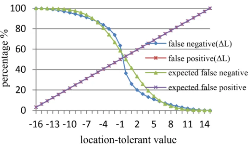
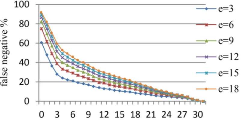
5.17 False negative and false positive rate related to location-tolerance . . . 91
5.18 False negative and false positive rate related to weight-tolerance . . . 91
5.19 False positive of different shift spaces . . . 92
5.20 False negative of different bit errors with different location-tolerance . . . . 93
5.21 False negative of different bit errors with different weight-tolerance . . . 93
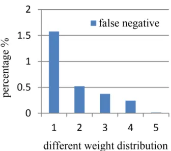
5.22 False negative of different weight distribution methods . . . 94
5.23 False positive and false negative rates of different 2048 location shift methods 95 5.24 Effect of response bias on false positive and negative rates . . . 96
5.25 Performance comparison of different fault tolerant methods . . . 97
5.26 Overall effect of number of errors . . . 97
6.1 Our PUF-based authentication design using PIT . . . 109
6.2 3D distributions of counter values and the floating threshold generation of three states for the RO PUF responses . . . 116
6.3 Possible location distribution of larger states and smaller states based on two groups of RO PUF test results . . . 118
6.4 Helper data generation for our floating thresholding key generation solution 120 6.5 PUF tests with temperature variation instrument . . . 124
6.6 Inter-PUF hamming distances . . . 126
6.7 Intra-PUF hamming distance . . . 127
7.1 Topology of FLSH network . . . 138
7.2 Basic FLSH cell structure in a CLB . . . 140
7.3 FLSH array with 16×16 cells . . . 142
7.4 Basic FLSH cell placement . . . 143
7.5 Critical wire routing among cells . . . 144
7.6 Cell reconstruction and hash regeneration of max-min pooling . . . 146
7.7 Weight distribution of convolutional weight algorithm . . . 148
7.8 The sample of FLSH output from Xilinx integrated logic analyzer . . . 149
7.9 The relationship between the sampling time and the different bits in the output150 7.10 Comparison of 32×32 bitmap with random inputs on an FLSH . . . 151
7.11 Probability of ‘1’ in the bitmap of FLSH . . . 152
7.12 Comparison of 32×32 bitmap with the same input on an FLSH . . . 152
7.13 FLSH output instability with different input errors . . . 153
2.1 Different PUF Performance Comparison . . . 18
3.1 FPGA Resource Usage of the Traditional RO PUF and the Optimized PCPUF Implementations . . . 41
3.2 Results of NIST Randomness Tests . . . 42
3.3 Bit Error Rate of RO PUFs and PCPUFs . . . 44
3.4 Bias of RO PUFs and PCPUFs . . . 45
4.1 False Positive and False Negative of USR-based Authentication . . . 58
4.2 Performance of ECC-based Authentications . . . 59
5.1 Performance of Different Bit Group Selection . . . 68
5.2 Security Comparison of Different Schemes - Number of response guesses required to achieve 50% or 99.9% success rate . . . 87
5.3 16×8 Bits ECC/BF Authentication Results . . . 89
5.4 128×1 Bits ECC/BF Authentication Results . . . 90
5.5 Performance Comparison of Our Solutions . . . 99
5.6 Overall Comparison with Other Solutions . . . 100
5.7 Performance of RWA with Real PUFs . . . 101
5.8 False Negative of Bit-by-bit Comparison . . . 102
6.2 Protocol of Our Authentication Method . . . 110
6.3 FPGA Resource Usage of One PUF Implementation . . . 125
6.4 Average Bit Error Rate . . . 128
6.5 Results of Authentication with PIP . . . 130
6.6 Overall Comparison of Error Correction and Bit Selection Helper Data Al-gorithms . . . 131
6.7 Performance Comparison of Floating Thresholding Solution with Helper Data on Four Different Types of PUFs . . . 133
7.1 Logic LUT Output of A Random FLSH Cell . . . 141
7.2 Performance of FLSH-based Similarity Search . . . 154
7.3 Performance of FLSH-based Clustering . . . 155
Introduction
In recent times, electronic devices have become so popular in our life, making people
rely on the safety and security of those embedded systems and IoTs. When we store our sensitive information on these untrusted devices, the system vulnerabilities offer the at-tackers great opportunities of obtaining individual information. Unfortunately, though
many conventional solutions have been applied to improve the security level, there are always new adversaries developed. As a fundamental reason, the vulnerabilities come from the hardware design and supply chain. To solve the problem, physical unclonable
functions (PUF) are recommended as a secure solution of authentication, random num-ber generation and key generation, which provides multiple features against hardware and software attacks. By implementing PUFs in the systems, commercial products
overcome the traditional security shortages to a certain degree.
1.1 Security Vulnerabilities of Embedded Systems and IoTs
Not as much work has been done in secure system design despite its importance in establishing security and trust for embedded systems, SoCs, and IoTs. The vulnerabili-ties of these systems include physical tampering, malware attack, information leakage,
and other aspects. The main threat of hardware is the counterfeit chips in the supply chain, which contains processors (ASICs, FPGAs, and microprocessors), nonvolatile memories (Flash memories, ROM, and RAM), IPs, and PCBs. As a consequence,
ef-fective protocols are required to authenticate and authorize each component in the sys-tem during the initialization. Apart from countermeasures, a secure hardware should also consider some methods against the probing attacks, snooping attacks, hardware
Trojans, power analysis attacks, electromagnetic attacks and machine learning attacks. On the software side, there are brute-force attacks, man-in-the-middle attacks, buffer overflow attacks, fault injection attacks and others. To protect the system, people de-veloped secure programming languages with trusted compiler and libraries, architecture and OS based countermeasures, static and dynamic code analyzers, and sandboxing
ap-proaches. Nevertheless, a system level design flow with security consideration has not been discussed widely yet.
1.2 Hardware Security Components
As we know, the traditional security solution mainly relies on the cryptography
devel-oped side-channel attacks against many hardware cryptography implementations. In-stead, trusted platform module has been proposed as a complex security solution in the
computer system. However, such a high-cost design cannot be applied to lightweight embedded systems or IoTs. Meanwhile, different true number random generators (TRNGs) have been proposed these years. Hardware RNG can be used for key generation in
cer-tain applications, but it does not provide deterministic results. Thus, the application is limited. Another security related module is one-way hash function. Though it is deterministic and stable, complex computation is required.
To overcome the limitation of those existing methods, researchers tried to use the random process variations that are generated during the manufacturing process. Since the components and circuits on the board have their own uncontrollable parameters, it is
possible to use the uniqueness to create unpredictable response. With this consideration in mind, physical unclonable functions were proposed by Gassend et al [1]. As a phys-ical component, a PUF is very hard to duplicate or predict due to the results of random
uncontrollable variables in the manufacturing process. When a PUF receives a chal-lenge, it reacts with a response, which is known as a Challenge-Response Pair (CRP). An ideal PUF-based CRP provides strong advantages in that each response gives
neg-ligible information on the responses from different challenges to the same PUF or even identical challenges on different PUFs [2]. Rather than storing secrets in non-volatile memories, PUFs can provide significantly higher physical security by generating these
PUF” or a “weak PUF”. The fundamental difference between weak and strong PUFs is the number of unique challenges that the PUF can process [4]. Both contain the
same characteristics including randomness, uniqueness, and reliability. A PUF pro-vides random output according to different input by involving the physical variations in the manufacturing process. This is significantly important in random number and
secure key generation. Secondly, the output of PUFs must be unique. Given the same input, two PUFs output different values. As a result, it is hard to predict the responses of one PUF even if all the data is tested on another PUF. Finally, an ideal PUF should
generate deterministic output, which is the basic requirement of key generation and au-thentication applications. Therefore, PUFs can be applied as a source of random but reliable data for applications such as generating unique IC identification numbers or
encryption keys.
1.3 Problem Statement
Though PUFs have many advantages, it is not a perfect primitive for security applica-tions. The biggest challenge of using PUFs is its instability in the output. It is essential
that the PUF responds with consistent results given the same challenge. However, most PUF constructions are not 100% reliable. Because the physical variations have very limited effect on the output, the result sometimes stays in a metastability condition. Meanwhile, temperature, voltage, and other factors affect the stability to some degree. For TRNGs, bit errors may be positive and acceptable. However, authentication and
key generation applications require deterministic values in most scenarios. The high raw bit error rate (RBER) in the responses of PUFs needs strong error correcting codes
(ECC) to guarantee a low false negative rate. However, a strong ECC requires large memory space and high calculation complexity. When the decoding demands are large enough, electronics systems with limited computation and storage capabilities may not
be able to afford the burden. As a result, traditional PUFs may not offer enough reli-ability for industrial applications. In this work, we will mainly discuss how we solve the instability of PUFs. Multiply solutions are offered to address the problem under different applications and requirements.
1.4 Related Works and Limitation
To solve the instability issue of PUFs, post-processing methods are widely involved. Since security-critical products require very low bit error rate of their cryptographic
keys, those optimized PUFs cannot be used directly as key generators. Therefore, var-ious HDAs have been proposed to maximize the stability in PUF responses. As indus-trial practical solutions, error correction schemes ensures the key to be reproducible [5].
For example, Bose-Chaudhuri-Hocquenghem (BCH) codes can provide high accuracy by encoding and decoding data with large arrays [6, 7]. However, ECC also means heavy redundancies. When the key length grows, the required codeword can be
ex-tremely large while the decoding time becomes significantly long. This redundant data also leaks information about the PUF response itself leading to a potential security
vulnerability. Another disadvantage is that ECC has a strict limitation on the maxi-mum number of bits it can correct. Given a number of errors beyond its capability,
ECC will lose its functionality. Alternatively, bit selection schemes become popular re-cently [5, 8, 9]. As a lightweight soft-decision coding, the least reliable bits in responses are discarded during the bit selection process. The most intuitive idea is to impose a
global threshold and filter out all mismatched bits. Relatively, local thresholding retains only the most reliable bits [5]. However, those algorithms have poor resistance to the variety of models caused by process variation or environmental noise. The reason is
that some unstable bits will either cross the threshold or change the sequence, which means former models are no longer suitable. As a result, it is hard to regenerate the same bit set with the original sequence, and no bit errors cannot be guaranteed.
Ac-cording to the HDAs described above, both error correction and bit selection schemes are not satisfying in term of PUF stability improvement.
1.5 Contributions
In this work, we devote the main paragraph to the design and algorithm of PUF
sta-bility, which includes the optimization design, implementation, various authentication solution, and key generation method. Specially, the contributions are list as follows:
1.5.1 PUF Design Optimization and Implementation
We optimize the traditional PUF design by replacing the challenge register with a shift
register or hash function. We also modify the architecture for timing improvement. Details of implementing PUF on FPGAs are discussed. Furthermore, a phase calibrated PUF is proposed to reduce the bit errors.
1.5.2 Post Processing Authentication Algorithm
We propose several authentication algorithms for different scenarios. Ring weight al-gorithm is a lightweight solution with limited computation, overhead, and accuracy. PUF initialization table provides very low false negative and false positive, though the calculation amount is much larger than RWA. Unstable-stable response is a trade-off between those two methods.
1.5.3 Solution for Key Generation Applications
By recording the feature of PUF in PITs, a floating thresholding key generation al-gorithm is discussed in this work. We involve both bit selection and error correction methods in the solution to improve the stability as much as we can. Meanwhile, security
problems are also considered since it is a critical factor of the application.
1.6 Thesis Outline
• Background
• PUF Design Optimization and Implementation
• Secure Authentication Solution with PUF Response Instability
• PUF Initialization Table for Robust Authentication and Key Generation
• Ring Weight Algorithm for Lightweight Authentication
• Locality Sensitive Hash Function for Identification and Clustering
Background
Physical Unclonable functions map a set of inputs (challenges) to a set of outputs
(re-sponses) which are called challenge-response pairs (CRPs). During the PUF design and implementation, we make use of random variations of manufactured structures to derive an uniquely individual behavior for each Integrated Circuit (IC). In order to
har-ness theses PUF properties, these individual variations must be extracted and mapped; which is almost impossible since process variations and noises are not clonable. PUFs came to the stage at a time when traditional cryptography failed to stand its ground
against physical attacks, side-channel attacks, etc. A significant advantage of PUF-based authentication is that unlike traditional key-PUF-based cryptographic systems, a PUF does not require the storage of secret keys in non-volatile memory. Instead, the secret
key is hidden within the physical body (e.g. intrinsic properties) of the circuitry which is found to be unclonable and unpredictable. In this chapter, we will introduce several popular PUFs.
2.1 Strong and Weak PUFs
PUFs are usually classified into strong and weak depending on the number of challenge-response pairs (CRP) that they can handle. Weak PUFs support a small number of CRPs which are linearly related to the number of components used to build the PUF. They
possess essentially a single, fixed challenge, as for example in the case of SRAM PUFs and DRAM PUFs. Strong PUFs, on the other hand, support a large number of CRPs such that polynomial time attacks become unfeasible. The lack of access restriction
mechanisms on strong PUFs is therefore a key difference from weak PUFs. These type of PUFs are usually employed for device authentication applications. As with any embedded system design and IoT devices, there is an inherent trade-off between the constraints of the operational environment and the desired functional capabilities of the device.
2.2 Ring Oscillator PUF
A ring oscillator PUF (RO PUF) is a typical example of delay PUFs whose instabil-ity has been heavily studied but remains unsolved. Figure 2.1 shows the traditional RO PUF design, which contains an array of ring oscillators (RO), two multiplexers
(MUXes), two counters, and a comparator. Because of manufacturing variations, the wire delay of each RO is not controllable, which leads to different frequencies of the RO output. By selecting two ROs according to the PUF input, we can measure the
the larger value than the second one, the PUF output is ‘1’. Otherwise the PUF output is ‘0’. Ideally, the output keeps the same bit value giving a certain input, but in reality bit
errors and bias are involved in the output. Though the systematic or correlated process variation and the environmental noise caused by the voltage and temperature variations degrade the output stability [10], the bit errors of FPGA-based PUFs are directly
gen-erated by a selected pair of ROs with close frequencies, which lead to the unstable measurement in the counters and the flipped output in the comparator. In [11], RO PUFs are characterized over 125 FPGAs. To improve the quality of ROs, the
surround-ing logic effect on the oscillator frequencies was studied and a strategy was proposed by placing and comparing ROs in a chain-like structure [12]. A reliability-improvement technique was used in pre-quantization phase of RO PUFs to reduce the noise in PUF
responses [13]. More optimized approaches were mentioned in [14] by introducing configurable ROs. They also suggested to compare adjacent RO pairs by controlled RO placement, but the FPGA implementations were not clear. A group-based RO PUF was
introduced in [15], which described a framework to filter the systematic variation and improve the hardware efficiency. However, its responses still required ECC.
2.3 Arbiter PUF
The arbiter PUF (APUF) is another typical delay PUF, which is widely studied and
evaluated [16]. An Arbiter PUF extracts the device-specific variation as delay diff er-ence between two selector chains. In another word, the generic idea behind arbiter
Fig. 2.1: The architecture of a traditional RO PUF
PUF is to race the delay times between two signals. The two signals propagate through
various routes depending on the value of the challenge. As shown in Figure 2.2, each challenge bit selects the input path of a MUX pair. Since the location of the MUXes are different, the input wire delay may not be exactly the same. The final value of the 1-bit response is determined by which signal arrives first. Thus, its output should be either ‘0’ or ‘1’, but it is unpredictable. Note that the pattern is also determined by the input length. If the challenge hasnbits, the propagation delay time should have 2n
combinations. Early work on Arbiter PUF modeling attacks had described successful approaches already, including the standard Arbiter PUF, XOR Arbiter PUF, lightweight PUF, and Feed-Forward Arbiter PUF [17, 18].
2.4 Bistable RO PUF
Similar to an SRAM cell that contains a pair of cross-coupled inverters, the bistable RO PUF (BR PUF) is based on the fact that an inverter ring consisting of an even number of inverters has two possible stable states. Figure 2.3 shows an example of a 64-stage BR
PUF [19]. Each stage contains two NOR gates, a DEMUX as gate input, and a MUX as gate output. Thus, when a 64-bit challenge is received by this BR PUF, either the upper or the lower paths of the MUX and DEMUX are selected. When we apply different challenges, different combinations of NOR gates and paths are selected as a result. In Figure 2.3, the total number of input patterns is 264. In order to generate a response,
the whole PUF needs to be reset as “high” first. After the challenge is applied to the
bistable rings, we wait until the bistable rings to be ‘0’. A reset of “low” is launched afterwards. Then we wait for some time to let the bistable ring stabilize. Finally, we
read out a 1-bit response. To generate more bits for responses, we repeat the progress for certain loops.
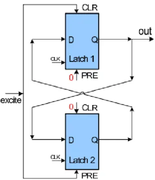
2.5 Butterfly PUF
A Butterfly PUF (BPUF) includes a cross-coupled circuit, which is brought to the un-stable state until it becomes un-stable. To make it clear, a cross-coupled circuit provides a positive feedback to record the value in a loop. It has two stable state and one unstable
state. The unstable state can be easily changed to one of the stable states by a certain input. The behavior of BPUF is similar to the SRAM cell. As Figure 2.4 shown, the structure of 1-bit BPUF is as simple as two latches [20]. When the input signal is set
to high, the BPUF becomes unstable at the beginning. If the input is set to low then, the BPUF turns to be one of the stable state, with an output of ‘0’ or ‘1’. The final state only depends on the wire delay of the circuit. Originally, since attackers cannot
measure the internal delay of an FPGA or ASIC directly, it is hard to predict which state the BPUF is in. However, as the side-channel attacks become popular, they brings
new vulnerabilities to BPUFs.
2.6 DRAM PUF
DRAM PUF (DPUF) was recently proposed as a new type of PUF [21, 22], compared to the widely studies of SRAM PUF [8, 23]. According to Figure 2.5, there are three
approaches to use DRAM as PUFs. The first one makes use of the built-in-self-refresh module of DRAM chips. As we know, DRAM not only requires a power supply to retain data, but must also be periodically refreshed to prevent their data contents from
Fig. 2.4:The architecture of a typical butterfly PUF
all cells to ‘1’ and then turn offwith refresh. Some cells will leak to ‘0’ while others are still ‘1’. Another approach is to use the remanence of DRAM cells. When a DRAM powers off, the data fades away over time in a random way. Thus, the remanence effect can also be applied to PUF. The final method is to use the startup value of DRAM.
During startup, the storage capacitor has neither been charged nor discharged. Thus the voltage of the capacitor is equal to the bias voltage. Because of the manufactur-ing variations, the capacitance will be slight different, which means a random value assignment.
Fig. 2.5: The meory structure of a DRAM array
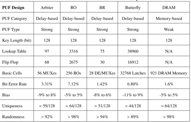
2.7 Performance Comparison
Table 2.1 shows different types of implemented, and designed, PUFs performance com-parison in details. As shown in this Table, the first column demonstrates various per-formance metrics that need to be considered for each PUF in order to evaluate the effectiveness of each design. Note that the data of RO, abiter, BR, and butterfly PUF are from our implementation and measurement. We also list the memory-based PUF as a comparison. One should notice that the other major difference between the first four presented PUF designs and the fifth (DRAM) PUF is that the “PUF Type” differs between strong (large number of CRPs) and weak (small number of CRPs). The next metric that we evaluated was “Key length”, which was “128 bits” for every one of the PUF designs we examined. The “lookup table” and “flip flop” rows show the number of those elements used to implement each PUF solution on an FPGA. One should note that
DRAM has no values for this, since it is implemented using a commercial offthe shelf (COTS) DRAM memory and not an FPGA. The “basic cells” row show the number of cells and type of cells (e.g. multiplexers, ring oscillators, inverters, demultiplexers, flash, memory) that we required to implement each PUF solution. The next metric we evaluated each PUF design using was “bit error rate”; defined as percentage of bit flips that occur. One should note that this is a good representation of the stability of each type of PUF. The “bias” represents the percentage of 1s and 0s in the generated output. Please note that the presented bias is in terms of the number of 0s present in the output.
The following metric, “uniqueness”, is a measure of how uncorrelated the response bits are across multiple implementations of the same PUF design. Ideally the response bit should differ with a probability of 50%. A key point to make on the uniqueness pre-sented is that the RO and DRAM PUFs have a difference of half the bits (e.g. 50%). The last property is “randomness”; a measure of the unpredictability of the response bits. For our proposed PUF, the randomness results show promising capability of our
new models. From this table of data we are able to compare and contrast the various solutions to determine those most favorable to any given scenario.
2.8 Contributions
In this chapter, we introduce five types of PUFs: Ring Oscillator PUF, Arbiter PUF,
Bi-Stable PUF, Butterfly PUF, and DRAM PUF. The details of design and implementation are discussed in each section. Finally, we compare the performance of these PUFs. The
Table 2.1: Different PUF Performance Comparison
PUF Design Arbiter RO BR Butterfly DRAM
PUF Category Delay-based Delay-based Delay-based Delay-based Memory-based PUF Type Strong Strong Strong Strong Weak Key Length (bit) 128 128 128 128 128 Lookup Table 97 3316 75 38960 N/A
Flip Flop 68 2675 30 16912 N/A
Basic Cells 56 MUXes 256 ROs 28 DE/MUXes 32768 Latches 921 DRAM Memory Bit Error Rate 3.31% 7.12% 1.42% 6.80% 1.6% Bias -9% to 8% -5% to 5% -8% to 6% -11% to 9% -5% to 5% Uniqueness ≈59/128 ≈64/128 ≈51/128 ≈44/128 ≈64/128 Randomness >92% >98% >94% >89% >98%
PUF Design Optimization and Implementation
3.1 Introduction
Researchers have developed different types of PUFs since the concept was proposed [11, 16, 19, 20, 22]. Among those PUFs, RO PUF is a well-known type with typical perfor-mance. Its architecture can be easily implemented on digital circuit. Therefore, in this chapter, we focus on a practical RO PUF implementation on FPGAs. We optimize the
architecture of RO PUFs and show the details of implementing RO PUFs on FPGAs. To improve the measurement accuracy of RO frequency, we use phase calibration pro-cess for frequency estimation. Meanwhile, We also minimize hardware resources and
develop a flexible output data width. Furthermore, we explore the feature of instability in PUF responses and provide a new design that outputs stable bits according to the unstable RO pairs.
3.2 RO PUF Description and Properties
Problem Analysis
Few papers have discussed the impact of bias in RO PUF responses [14], which is
the favoring of RO PUFs to either 1 or 0. According to our tests, we found that the counter design in the traditional RO PUF can contribute significantly to this bias. When
CounterAandCounterBhold the same value, the comparator must make an choice of how to treat this case - in our example, the comparator puts this “equivalent” case in the “smaller” group.. The “larger” group, on the other hand, can be active only when
CounterAreceives more pulses thanCounterB in the given clock cycles. Therefore, the output contains more 0’s than 1’s. If ROs are placed more regularly, the frequencies may end up being closer, thus causing more ”equivalent” cases. This is aggravated especially when the counter size is limited. Regardless of the count cycles, the bias
caused by the counter design is still as high as 5.03%. As a result, the bit error rate and the bias are intensified by the design fault and inaccurate measurement. Another problem of this RO PUF design is the inefficient usage of hardware resources. To generate just a single bit output, the design requires an logN-bit input andNoscillators. Though we can apply a hash function to generate different challenges, its hardware implementation requires even more FPGA slices than the PUF itself [24]. A transient
effect ring oscillator PUF was proposed with a good ratio of PUF response variability to response length, but the intra-device variation increases to 1.7% [25], compared to [11]
with 0.86% intra-device variation. In this chapter, we will discuss a practical phase calibration technique to improve the quality of RO pairs comparison, which shows a
trade-offbetween the cost, stability, and flexibility.
3.2.1 RO PUF Design Improvement
Though RO PUFs have been heavily studied, there are still possibilities of improvement particularly with respect to implementations on FPGAs. In this section, we will discuss some practical RO PUF optimizations on the hardware.
Ring Oscillator Design on FPGAs
While PUFs have been primarily targeted towards ASIC designs, we explore their
po-tential on FPGAs. According to our test on the Kintex-7 FPGA [26], the frequency of a 5-stage inverter chain RO is approximately 475 MHz when the system clock is 200 MHz. In the crossing timing domain between the ROs and PUF control logic circuit, a
high RO frequency adds to the instability of measurements. As with all oscillators, the rate of oscillation is determined by the length of a delay implemented in a loop. Thus, to reduce the frequency, more inverters can be added in the ROs, but it requires more
hardware resources. We provide an improved RO design that takes advantage of the lookup tables (LUTs) of the configurable logic blocks (CLBs) and the general purpose interconnect [27] in the FPGA. As shown in Figure 3.1, the first part consists of a
of all LUTs. In the second part, a single inverter in the loop implements a high gain inverting amplifier. The output frequency is divided by 2 in order to eliminate output
glitches. This design only needs six LUTs and a D-type flip-flop (FD).
Fig. 3.1:An improved RO design for an FPGA
Shift Register and Hash Function for Resource Improvement
In order to generate variable length responses, we choose a design as shown in
Fig-ure 3.2. This example uses 128 ROs to provide 128-bit CRPs. Once a challenge is received, it is stored in a shift register. We select the first 7 bits from the register as the input of the upper decoder and MUX in order to select an RO from the array. Likewise,
another RO is selected using the next 7 bits from the challenge shift register. If the ad-dresses are the same, the second 7-bit address is added by 1 to avoid selecting the same RO for comparison. Next, we shift the challenge register to select a new RO pair. The
shift pattern can be complex for security consideration. To make it easy to understand, we shift one bit to the left each time. If the challenge is 128 bits, we can generate a 128-bit response with 127 shift operations.
Alternatively, the shift register can be replaced by a non-cryptographic hash func-tion. Compared to cryptographic hash function, which provides one-way, collision
re-Fig. 3.2: Architecture of our RO PUF
sistant, and deterministic properties, non-cryptographic hash function is significantly
faster and low-cost. It is also easy to be implemented on FPGAs. Below is the algo-rithm of ElfHash that we used in the PUF:
Timing Improvement
In the traditional design, metastability can exist at the input of the counters. It occurs when the counters receive a clock rising edge for comparison. If the RO output happens
to flip when a counter value is changing, the result of comparison will be none of larger, smaller, or equal, but a metastable state. We have verified this scenario on our FPGA implementations. As a result, the instability of responses increases. Our solution is to
use two registers to store the counter values. The registers and counters are in the same clock domain so that metastabilities are eliminated. The comparison result is recorded in the response register as an output bit.
Algorithm 1ElfHash process 1: procedurePCP 2: hash←0 3: x← 0 4: count ←0 5: loop 1: 6: hash←(h<<4)+challenge 7: challenge←challenge+1
8: if x=hashand 0xF0000000then
9: hash←hashxor (x>>24) 10: hash←hashand (notx) 11: count ←count+1
3.2.2 RO PUF Implementation on an FPGA
Few papers have clear descriptions on how the RO PUF is implemented on FPGAs [14,
28, 29]. Incorrect HDL coding can lead to logic unit rebuilding during synthesis, which results in functionality failure. For example, inverters built with inv(1) <= not inv(0);statements will be optimized out and cannot be placed as RO arrays.
LUT-based RO Placement
To implement the ring oscillators on FPGAs, we use the LUTs directly in our code and
add element placement constraints to fix the LUTs with certain delay. In our work, we used the Vivado development kit and the Kintex-7 FPGA provided by Xilinx to show the RO PUF implementation on FPGAs [26, 30]. In the Kintex-7, a CLB contains a pair
of slices, and each slice is composed of four 6-input LUTs and other elements [31]. By setting the initial value to “01”, a 1-input LUT (LUT1) can perform the same function as a digital inverter. An example of the traditional RO implementation is shown in
Figure 3.3. We place one LUT3 (3-input LUT) in the left slice and four LUT1’s in the right slice. These five LUTs and the white connections form a basic RO. Apart from the feedback input of another inverter, LUT3 also includes a reset input and an enable
input. The left LUTs in a CLB are reserved for other logic of the RO.
Figure 3.4 shows the RO placement given by Figure 3.1. Four delay LUT2s are placed in the left slice and the invert LUT locates in the right slice. The output of the
Fig. 3.3:LUT-based RO placement example
LUT2 in the right slice. Since the delay LUTs contain no logic, ‘keep’ attributes is required in the design to stop logic optimization by the synthesis tool. Additionally, a
combinatorial loop in the FPGA is considered bad design practice in most cases, which increases the number of cycles by infinitely going around the circle in the same path. To avoid unnecessary errors during synthesis and bitstream generation, some constraints
are applied to let Vivado ignore these loops.
Fig. 3.4: Improved LUT-based RO placement example
RO Array Placement on FPGA
Figure 3.5 shows the manual placement of one RO PUF. To maintain the randomness
are listed in six columns regularly in order to maximize the manufacturing differences between PUFs. Between columns, two slices are reserved for the relevant logic between
ROs and the control unit. LUTs and FDs of the finite-state machine (FSM) are placed at the bottom of the RO array. Other primitives with no effects on the performance are placed by Vivado automatically.
Fig. 3.5: RO PUF manual placement overview
Automatic Constraints Generation
However, manual placement of PUFs can be very time-consuming. In our example,
each RO array contains 768 LUTs and 128 FFs. If the hardware specification is modi-fied, it may lead to the reconstruction of the architecture. As a result, most of the cells have to be placed again. To make it progress more efficient, we developed an automa-tion code generaautoma-tion process in Figure 3.6. The hardware specificaautoma-tion module defines the length of CRPs, performance requirements, and usable platforms. The information
is translated to acceptable format of Shell script so that the code generation script can figure out the scale of RO array. With pre-defined templates, we are able to generate
the code and constraints automatically.
Fig. 3.6:RO PUF code generation
Manually Rounting Consideration
On the other hand, improper routing also affects the uniqueness of PUFs. Though our LUT and FF placement fixes the RO routing path, the other parts are routed by Vivado automatically. The critical paths are the RO array enable and the counter enable. If
the RO array enable has a long delay while the counter enable has a short delay, it indicates that the timing to generate RO pulses is postponed and the counter is enabled in advance. In consequence, the window for measurement may not match the RO output
well, which leads to potential issues of uniqueness and bias. To eliminate the effect of expected delay, we adjust unsatisfied wire delay by changing paths manually in Vivado implementation and saving it as constraints.
Stability Analysis
A key metric of any PUF is its reliability. In order to evaluate the stability, we have
implemented three RO PUFs on the FPGA, which are based on Figure 3.2. We gen-erated 100,000 random challenges and applied the challenge twice to each PUF. The two responses for each PUF were compared and the Hamming distance between the
two responses were recorded. Ideally, there should be no difference between the two responses because the challenge was the same and the Hamming distance should be zero. Figure 3.7 shows the Hamming distance distribution for the three PUFs. Without
any error correction or fault tolerance methodology, there are about 10 bit errors in each 128-bit response. It is clear that a 7.81% bit error rate is unsatisfactory for authentica-tion. Without very strong ECC, we will have a high false negative rate. To address the
instability of PUFs, we will introduce a phase calibration process in the next section.
−50 0 5 10 15 20 0.02 0.04 0.06 0.08 0.1 0.12 0.14 0.16
Number of bit errors
Probability PUF1 fitting curve PUF2 fitting curve PUF3 fitting curve
3.3 Phase Calibrated PUF
Improving the stability of PUFs requires an accurate measurement of the RO frequency. With the traditional RO PUF, theoretically, one could use a longer measurement time to count RO pulses and thus improve the measurement accuracy.. However, we found
that extending the measurement time from 16 clock cycles to 512, in order to get larger samples, had limited improvement on the stability. Since the ROs are not driven by the system clock and each enable signal has its own delay, the output can be unstable when
the counter is enabled and disabled [12]. As a result, the count may be offby one or two. Previously, we discussed adding a counter register to eliminate the unknown state, it does not address the correctness due to instabilities at the boundaries of the
measure-ment cycle. Due to this unpredictable behavior, even though we tested some “stable” RO pairs 1,000 times and got the same results every time, the next measurement might
still produce different value with a small probability. In this section, we propose an effi -cient solution instead of the repeated testing, which can solve this problem with limited cost.
3.3.1 Phase Calibration Process
Phase Calibration IP Core
The phase calibration process (PCP) is a critical part of our solution, which aims to
measure the frequency of ROs fast and accurately. The basic idea is to shift the phase of the RO output signal in order to eliminate asynchronous timing measurement error.
To implement it on FPGAs, we use a primitive that offers a programmable delay func-tion, i.e. Xilinx provides an input delay resource called IDELAYE2 [32]. It can be
accessed directly from the FPGA logic and allows incoming signals to be delayed on an individual input pin basis. Figure 3.8 shows the IDELAYE2 primitive, which offers a variable delay mode that can control the delay value after configuration by
manipu-lating the control signals CE and INC. When CE goes High, the increment/decrement operation begins on the next positive clock edge. The programmable delay taps in the IDELAYE2 primitive wrap-around. When the last tap delay is reached (tap 31) a
sub-sequent increment function will return to tap 0. In Figure 3.8, a reset is detected (LD is High) in the first clock event, causing the output DATAOUT to select tap 0 as the output from the 31-tap chain. In the second clock event, a pulse on CE and INC is
captured on the rising edge of C. This indicates an increment operation. The output changes without glitches from tap 0 to tap 1. In the third clock event, CE and INC are no longer asserted, thus completing the increment operation. The output remains at tap
1 indefinitely until there is further activity on the LD, CE, or INC pins.
Architecture of Phase Calibrated PUF
The architecture of our phase calibrated PUF (PCPUF) is shown in Figure 3.9. It mainly
consists of a 128-RO array, a control unit, a comparison unit, and pair of decoders, MUXes, IDELAYE2s, and counters. The tap control is to control the delay of IDE-LAYE2. Since PCP requires a strict RO enable timing, only one selected RO pair is
enabled in the measurement period. Otherwise, the control unit resets all the ROs.
Fig. 3.9:Architecture of PCPUF
PCPUF Algorithm
Algorithm 4 shows the details of the PCP. In order to generate a 1-bit response, the first two 7-bit values of the challenge register are loaded to the registeraddr Aand register
addr B. After checking the values, we resetCounterA andCounterB. The tap value is loaded to IDELAYE2 primitives before being added by 1. By default, the tap value is 0. When the delay is set, the control unit enables the selected RO pair and starts
testing. Each measurement takes 16 clock cycles. Then the tap value is added by 1 and the new measurement starts. Between two measurements, the selected RO pair is kept
disabled before the delay is set. When we complete the test from tap 0 to tap 31, a 1-bit output is generated by comparing the counter values. Then the challenge register shifts
its value and launches the next response generation. Though the PCP slows down the response generation comparing to the traditional RO PUFs, the PCPUF still keeps an output speed of 625,000 bit/s.
3.3.2 Analysis of Phase Calibration Efficiency
Considering the calculable factors of FPGA, the accuracy of frequency estimation by
using the phase calibration process depends on the skew rate, threshold voltage, and the relevant signal cycle. The skew rate and the threshold voltage determine the skew between the system clock and the counters. When the control unit enables or disables
the counters at the beginning or in the end of the phase calibration process, the RO outputs may be changing between the voltage thresholds,VOH minandVOL max. This may
lead to a metastable state of the counter value. According to the I/O buffer specification (IBIS) model of the Kintex-7, if the FFs are in the same bank, the skew should be 50 ps to 100 ps. The internal signal voltage of the Kintex-7 is designed to swing between -0.5 and 1.1 volts, with anything below 0.4 volts considered a ‘0’, and anything above
0.7 volts considered a ‘1’ [33, 34]. In the worst case, the metastability duration of each rising edge or falling edge is 18.75 ps. Since the RO output phase at the beginning of the window is unpredictable, we can calculate the probability of the metastability
Algorithm 2PUF phase calibration process 1: procedurePCP
2: tap←0 3: loop 1:
4: resetCounterA,CounterB
5: loadaddr A,addr B
6: if addr A=addr Bthenaddr B← addr A+1 7: loop 2:
8: loadtaptoIDELAY E2 9: tap←tap+1
10: enableRO(addr A),RO(addr B) 11: loop 3:
12: enableCounterA,CounterB
13: readRO(addr A),RO(addr B) 14: if count cycle<16then gotoloop 3
15: keepCounterA,CounterB
16: disableRO(addr A),RO(addr B) 17: if tap< 32then gotoloop 2
18: ifCounterA>CounterBthen
19: output 1 20: else
21: output 0
22: shiftChallenge
prising edge = pf alling edge =
18.75ps×2
4210ps = 0.00891 (3.1)
in which 4210 ps is the average RO cycle. Though the rising edge and falling edge have the same probability, they are not independent events for any RO within one tap delay. Now we focus on the entire process in Figure 3.10. We create a window of 16
system clock cycles (80 ns), within which the counters of the RO PUF become active. Due to the wire delay, the selected RO pair may not be enabled at the same time. The delay between each RO and the related counter depends on a tap ranging from 0 to
31. Since each taps of IDELAYE2 offers 78 ps delay in the normal environment, we can have as much as 2.418 ns delay of the RO output, which is long enough to find the metastability. Ideally, these 32 taps phase shift will not affect the RO frequency measurement. However, some measurements show different counter values due to the metastability. According to our simulation, one metastability occurrence at one edge of the window has a probability of 0.00775. The probability that two metastability
occurrences at both edges of the window is 0.00113. There is no possibility of any more unpredictable states as the window only has two edges. Thus the expected value of metastability is
E[X]=1×0.00775+2×0.00113=0.01116 (3.2) Therefore, among the 32 taps shift cases, most of the counter values reflect the
frequency of the selected RO correctly. The metastability only happens with a very low possibility.
Fig. 3.10:PUF phase calibration timing
Apart from the calculable factors, measurement errors are also generated by the noise margin, which is the amount by which the signal exceeds the threshold for a proper ‘0’ or ‘1’. Being affected by the uncontrollable factors such as temperature, voltage, and aging effects, we can hardly calculate the fault tolerate capability of phase calibration process directly [35]. But we are able to obtain the probability of bit flipping after PCP through large amounts of tests. Next we estimate the efficiency of PCP by computing the intra-PUF hamming distance.
3.3.3 Estimation of Intra-PUF hamming Distance
The bit error rate is one of the most critical characteristic of PUFs. To estimate the
RBER of PCPUFs, we need to know the intra-PUF hamming distance first, which can be calculated through the distributions of RO frequencies and bit flipping rate (BFR). As we mentioned, when the frequencies of two ROs are closer, temperature, voltage,
and aging effects during operation lead to higher BFR. We begin with measuring the rising edges of ROs in the unit time and show the probability distribution in Figure 3.11.
The unit time is set to 80 ns (16 clock cycles). Since we add the measured data from tap 0 to tap 31 and compute the average value, the results may not be integral. A fitting
Gaussian curve is generated according to the discrete data, which is used to provide an ideal discrete distributionD(f) for our computation.
17 17.5 18 18.5 19 19.5 20 20.5 21 0 0.01 0.02 0.03 0.04 0.05 0.06 0.07 0.08 0.09 Rising edges of RO in 80 ns Probability measurement fitting curve
Fig. 3.11:Distribution of RO rising edges on average
We define a specific bit flipping rateλaccording to the difference of the discrete data. Marked as f1and f2, the frequencies of two ROs determine the probability of bit
flipping. A measuredλ(|f1− f2|) in Figure 3.12 shows the statistical BFR results, which
follows part of a normal distribution 3.61×10⁸N(−12.99,1.882). When two ROs have
a|f1− f2|larger than 1, their output is very stable. However, the BFR increases sharply
when the difference range is less than 0.5. To further improve the reliability of PUFs, these RO pairs can be blocked from the RO pair selection sets.
0 0.5 1 1.5 2 2.5 3 0 0.002 0.004 0.006 0.008 0.01 0.012 0.014 0.016 0.018 0.02
Difference of RO rising edges in 80 ns
Probability
measurement fitting curve
Fig. 3.12:Distribution of 1-bit RO output flipping rate
∞ X f2=0 ∞ X f1=0 D(f1)×D(f2)×λ(|f1− f2|)=0.0029 (3.3)
The probability that 128-bit responses contain exactlynbit errors is
128
n
!
0.0029n(1−0.0029)128−n (3.4) According to Equation 6.5, the ideal intra-PUF hamming distance is shown in Figure 3.13. Therefore, we can calculate the average number of errors, which is 0.3688 in a 128-bit response.
0 2 4 6 8 10 0 0.1 0.2 0.3 0.4 0.5 0.6 0.7 0.8 Bit error Probability measurement fitting curve
Fig. 3.13:Expected Intra-PUF hamming distance
3.4 PCPUF Evaluation
3.4.1 Experimental Setup
In this section, we present the measured data from six implemented PCPUFs on two
KC705 boards, as shown in Figure 6.5. The temperature of FPGAs is controlled at 30◦C according to the on-chip sensor and the voltage is 1.008V.
3.4.2 Hardware Resource Utilization
Table 6.3 lists the post-implementation primitive utilization of the traditional RO PUF
and the optimized PCPUF. We exclude UART and FIFO module in the design to make a fair evaluation. The overall utilization of our PCPUF are 0.58% of the look-up tables and 0.05% of the flip-flops on the Kintex-7 FPGA. This is significantly low-cost
com-pared to the traditional RO PUF design. If we apply the architecture in Figure 2.1, only 35 arrays can be placed on a Kintex-7 FPGA, which means four FPGAs are required to implement a 128-bit RO PUF. Since the shift register or hash function is used in the
design, only one array is needed to generate multi-bit responses.
3.4.3 Randomness
We applied 15 NIST randomness tests to evaluate the randomness of our PCPUF re-sponses. The p-values and proportions are listed in Table 3.2. As the p-values are all larger than 0.01, we accept the responses as random [36]. Though we use a
pseudoran-dom number generator to generate challenges, the proportions show that at least 98% sequences pass the tests.
3.4.4 Uniqueness
The evaluation of the uniqueness of PCPUFs is shown in Figure 3.15, which compares three groups of 100,000 128-bit responses. The responses are generated by
Table 3.1: FPGA Resource Usage of the Traditional RO PUF and the Optimized PCPUF Implementations
Ref Name
RO PUF
PCPUF
Functional Category
LUT1
514
2
LUT
LUT2
268
857
LUT
LUT3
175
55
LUT
LUT4
52
94
LUT
LUT5
273
30
LUT
LUT6
293
279
LUT
MUXF7
0
34
MuxFx
MUXF8
0
16
MuxFx
FDCE
20
16
Flop & Latch
FDRE
430
195
Flop & Latch
FDSE
1
1
Flop & Latch
CARRY4
7
9
CarryLogic
IBUF
4
4
IO
OBUF
2
2
IO
BUFG
1
1
Clock
IDELAYE2
0
2
IO
IDELAYECTRL
0
1
IO
Slice
647
365
CLB Slice
Utilization
1.26
0.71
%
Table 3.2: Results of NIST Randomness Tests
Statistical Test
P-value
Proportion
frequency
0.066882
0.98972
block frequency
0.213309
0.98972
cumulative sums
0.534146
0.98978
runs
0.739918
0.99075
longest run
0.031497
0.98939
rank
0.219646
0.98988
FFT
0.392456
0.98991
non-overlapping template
0.122325
0.98940
overlapping template
0.062947
1.00000
universal
0.599114
1.00000
approximate entropy
0.637119
1.00000
random excursions
0.778616
0.98902
random excursions variant
0.137809
0.98905
serial
0.039329
0.99161
linear complexity
0.534146
1.00000
converging to 64 - thus, there are 50% bits flipped on average. Therefore, the responses are unique. Moreover, we have compared the responses from six PUFs on two FPGAs
30 40 50 60 70 80 90 0 0.01 0.02 0.03 0.04 0.05 0.06 0.07 0.08
Mismatched Bit Number
Probability PUF 1 vs. PUF 2 fitting curve 30 40 50 60 70 80 90 0 0.01 0.02 0.03 0.04 0.05 0.06 0.07 0.08
Mismatched Bit Number
Probability PUF 1 vs. PUF 3 fitting curve 30 40 50 60 70 80 90 0 0.01 0.02 0.03 0.04 0.05 0.06 0.07 0.08
Mismatched Bit Number
Probability
PUF 2 vs. PUF 3 fitting curve
Fig. 3.15: Inter-PUF Hamming distance
3.4.5 Stability
As shown in Section 3.3, the average number of errors is 0.3688 in 128-bit responses,
which means the theoretical bit error rate is 0.29%. To verify that, we generated chal-lenges with a pseudorandom number generator. Each challenge is used twice in order
to provide two responses for comparison. The test was repeated 100,000 times. Fig-ure 3.16 shows the measFig-ured intra-PUF Hamming distance of our PCPUFs. Compared to the corresponding results with no ECC and phase calibration in Figure 3.7, the
fit-ting curves for PCPUFs have obvious shift to the left and approach the ideal bound in Figure 3.13.
Table 3.3 shows the average bit error rate of three shift register based RO PUFs
and six PCPUFs. Compared to RO PUFs, PCPUFs have obvious improvement on the response stability. Though the bit error rates are higher than the ideal bound, all the results are smaller than 1.00%. This is still acceptable if we take the measurement
0 1 2 3 4 5 6 7 8 9 10 0 0.1 0.2 0.3 0.4 0.5 0.6 0.7 0.8 0.9
Number of bit errors
Probability PUF1 fitting curve PUF2 fitting curve PUF3 fitting curve
Fig. 3.16:Intra-PUF Hamming distance with phase calibration
errors into consideration. Since we do not apply ECC in our PUFs, the bit error rate is low enough for authentication purposes. Within the temperature range of normal
testing environment, we observed no significant changes of the bit error rate.
Table 3.3:Bit Error Rate of RO PUFs and PCPUFs
FPGA 1
BER
FPGA 1
BER
FPGA 2
BER
RO PUF 1
7
.
10%
PCPUF 1
0
.
54%
PCPUF 1
0
.
37%
RO PUF 2
8
.
09%
PCPUF 2
0
.
85%
PCPUF 3
0
.
70%
RO PUF 3
7
.
13%
PCPUF 3
0
.
62%
PCPUF 2
0
.
91%
3.4.6 Bias
Ideally, there should be 50% 1’s and 50% 0’s in a response. However, our RO PUF implementation on Kintex-7 FPGAs have a bias ranging from 41% to 58% according
to our tests. As a comparison, we list the bias of PCPUFs in Table 3.4. Each result is based on the mean of 100,000 128-bit responses. Without any post-processing, all
six PUFs produce bias within±2% of ideal, which prove the effectiveness of the phase calibration on improvement the RO PUF bias.
Table 3.4:Bias of RO PUFs and PCPUFs
FPGA 1
Bias
FPGA 1
Bias
FPGA 2
Bias
RO PUF 1
40
.
85%
PCPUF 1
49
.
21%
PCPUF 1
48
.
72%
RO PUF 2
47
.
10%
PCPUF 2
49
.
77%
PCPUF 3
51
.
08%
RO PUF 3
58
.
42%
PCPUF 3
51
.
35%
PCPUF 2
50
.
14%
3.5 Conclusions
In this chapter, we demonstrated a practical design and implementation of RO PUFs on FPGAs. The phase calibration process focuses on improving the frequency
measure-ment techniques in the crossing clock domain area. By involving phase calibration, the 7.81% bit error rate is reduced to less than 1%. We also evaluate other properties of PCPUF, including randomness, uniquess, and bias.
Secure Authentication Solution with PUF Response Instability
4.1 Introduction
Authentication is widely applied in the digital world, which poses special problems
with electronic communication and supply chain device identification. It has vulner-abilities to man-in-the-middle attacks and counterfeiting. Previously we introduce a stable PCPUF design. Based on that, we will discuss a specific authentication
applica-tion using the instability of PCPUF in this chapter. Unlike the normal usage of PUF response, this work converts the unstable bits to the stable output. It is noted that the method can be applied to other types of PUF as well. Furthermore, an obfuscation
system is provided to enhance the security of authentication solution, which also takes advantage of the unstable response in PUFs.
4.2 Unstable-Stable Response
Modeling and machine learning attacks are well-known for PUF adversary. The
suc-cessful prediction is due to the accurate calculation and measurement of physical
rameters such as delay and frequency. To achieve a secure PUF-based solution against those attacks, we propose a novel method to generate responses, which uses the
insta-bility of PUFs. Since the unstable bits in the RO PUF response are hard to be predicted, they provides better security feature than the stable ones. However, those bits have been only considered in the random number generation application yet. For other scenarios,
only stable bits are usually required. In our work, we find the possibility to transfer the unstable bits to stable bits and apply them to PUF responses, which is present as unstable-stable response (USR), a more stable and secure response.
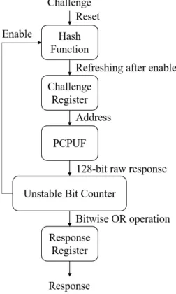
USR Generation
Figure 4.1 shows how to generate USR with a PCPUF. We set another hash function
module out of the PCPUF, which can provide multiply sub-challenges with only one challenge input. Once a sub-challenge is created, it is sent to the challenge register for temporary storage. By reading the value from the register, PCPUF selects two RO pairs
and keeps outputting the 1-bit response to the first address of the unstable bit counter for 1,000 times. The accumulated value in the counter reflects the stability of this output. A number that close to 0 or 1,000 is known to be stable while 500 is regarded as the
most unstable response. With the help of its internal hash function module, the model generates a 128-bit raw response and stores it in the counter. Since PCPUFs provide good stability in their responses, the obvious unstable bits are so limited that less than