High Current Density Surface-Mount
(TMBS
®
) Trench MOS Barrier Schottky Rectifier
Ultra Low V
F
= 0.49 V at I
F
= 5 A
LINKS TO ADDITIONAL RESOURCES
FEATURES
• Trench MOS Schottky technology
• Low forward voltage drop, low power losses
• High efficiency operation
• Meets MSL level 1, per J-STD-020,
LF maximum peak of 260 °C
• AEC-Q101 qualified available
- Automotive ordering code: base P/NHM3
• Material categorization: for definitions of compliance
please see
www.vishay.com/doc?99912
TYPICAL APPLICATIONS
For use in low voltage high frequency DC/DC converters,
freewheeling diodes, and polarity protection applications.
MECHANICAL DATA
Case:
FlatPAK 5 x 6
Molding compound meets UL 94 V-0 flammability rating
Base P/N-M3 - halogen-free, RoHS-compliant
Base P/NHM3 - halogen-free, RoHS-compliant, and
AEC-Q101 qualified
Terminals:
matte tin plated leads, solderable per
J-STD-002 and JESD 22-B102
M3 and HM3 suffix meets JESD 201 class 2 whisker test
Notes
(1) With infinite heatsink
(2) Free air, mounted on recommended pad area
(3) The heat generated must be less than the thermal conductivity from junction-to-ambient: dP
D/dTJ < 1/RJA
PRIMARY CHARACTERISTICS
IF(AV) 30 A VRRM 150 V IFSM 240 A VF at IF = 30 A (TJ = 125 °C) 0.68 V TJ max. 150 °C Package FlatPAK 5 x 6Circuit configuration Single
FlatPAK 5 x 6
4 3 1 2 5 6 8 7 1, 2, 3, 4 5, 6, 7, 83
33
D
DD
3 D
3D Models AvailableMAXIMUM RATINGS
(T
A= 25 °C unless otherwise noted)
PARAMETER SYMBOL V30K150 UNIT
Device marking code V3015
Maximum repetitive peak reverse voltage VRRM 150 V
Maximum DC forward current IF(AV)
(1) 30
A IF(AV)(2) 3.5
Peak forward surge current 8.3 ms single half sine-wave
superimposed on rated load IFSM 240
Operating junction temperature range TJ(3) -40 to +150
°C
V30K150
www.vishay.com
Vishay General Semiconductor
Revision: 04-Sep-2020 2 Document Number: 87157
For technical questions within your region: [email protected], [email protected], [email protected] THIS DOCUMENT IS SUBJECT TO CHANGE WITHOUT NOTICE. THE PRODUCTS DESCRIBED HEREIN AND THIS DOCUMENT
ARE SUBJECT TO SPECIFIC DISCLAIMERS, SET FORTH AT www.vishay.com/doc?91000 Notes
(1) Pulse test: 300 μs pulse width, 1 % duty cycle (2) Pulse test: pulse width 5 ms
Notes
(1) The heat generated must be less than thermal conductivity from junction to ambient: dP
D/dTJ < 1/RJA (2) Free air, mounted on recommended copper pad area; thermal resistance R
JA - junction-to-ambient (3) Mounted on infinite heatsink; thermal resistance R
JM - junction-to-mount
Note
(1) AEC-Q101 qualified
ELECTRICAL CHARACTERISTICS
(T
J= 25 °C unless otherwise noted)
PARAMETER TEST CONDITIONS SYMBOL TYP. MAX. UNIT
Instantaneous forward voltage
IF = 5 A TJ = 25 °C VF(1) 0.59 -V IF = 15 A 0.85 -IF = 30 A 1.30 1.40 IF = 5 A TJ = 125 °C 0.49 -IF = 15 A 0.60 -IF = 30 A 0.68 0.74 Reverse current VR = 100 V TJ = 25 °C IR(2) 0.009 -mA TJ = 125 °C 5 -VR = 150 V TJ = 25 °C - 0.35 TJ = 125 °C 11 35
Typical junction capacitance 4.0 V, 1 MHz CJ 1660 - pF
THERMAL CHARACTERISTICS
(T
A= 25 °C unless otherwise noted)
PARAMETER SYMBOL TYP. MAX. UNIT
Thermal resistance RJA
(1)(2) 75
-°C/W
RJM(3) 2.5 3.5
ORDERING INFORMATION
(Example)
PREFERRED P/N UNIT WEIGHT (g) PREFERRED PACKAGE CODE BASE QUANTITY DELIVERY MODE
V30K150-M3/H 0.10 H 1500 7" diameter plastic tape and reel
V30K150-M3/I 0.10 I 6000 13" diameter plastic tape and reel
V30K150HM3/H (1) 0.10 H 1500 7" diameter plastic tape and reel
RATINGS AND CHARACTERISTICS CURVES
(T
A= 25 °C unless otherwise noted)
Fig. 1 - Maximum Forward Current Derating Curve
Fig. 2 - Forward Power Loss Characteristics
Fig. 4 - Typical Reverse Leakage Characteristics
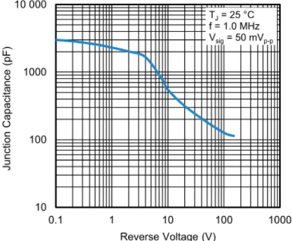
Fig. 5 - Typical Junction Capacitance
10 100 1000 10000 0 5 10 15 20 25 30 35 0 25 50 75 100 125 150 Axis Title 1st li ne 2nd li ne 2nd l ine A v erage Forw ard R e cti fi e d C u rrent (A ) Mount Temperature (°C) TMmeasured at cathode
terminal mount typical values
RthJM= 2.5 °C/W RthJA= 75 °C/W 10 100 1000 10000 0 2.0 4.0 6.0 8.0 10.0 12.0 14.0 16.0 18.0 20.0 22.0 24.0 26.0 0 5 10 15 20 25 30 35 Axis Title 1st li ne 2nd li ne 2nd li ne Ave ra g e Po w e r L o s s ( W )
Average Forward Current (A) D = 0.1 D = 0.2 D = 0.3 D = 1.0 D = tp/T T tp D = 0.8 D = 0.5 10 100 1000 10000 0.1 1 10 100 Axis Title 2nd li ne In stantaneou s Forw ard C u rrent (A ) TJ= 125 °C TJ= 100 °C TJ= 150 °C TJ= -40 °C TJ= 25 °C 10 100 1000 10000 0.00001 0.0001 0.001 0.01 0.1 1 10 100 10 20 30 40 50 60 70 80 90 100 Axis Title 1st li ne 2nd li ne In stantaneou s R e verse C u rrent (m A )
Percent of Rated Peak Reverse Voltage (%) TJ= 150 °C TJ= 125 °C TJ= 100 °C TJ= -40 °C TJ= 25 °C 10 100 1000 10 100 1000 10 000 0.1 1 10 100 1000 Axis Title 1st li ne 2nd li ne 2nd li ne Juncti on C apaci tance (pF) Reverse Voltage (V) TJ= 25 °C f = 1.0 MHz Vsig= 50 mVp-p 10 100 1000 10000 1 10 100 Axis Title 1st li ne 2nd li ne 2nd li ne T ransi ent T h erm a l I m pedance (°C /W ) Junction to ambient
V30K150
www.vishay.com
Vishay General Semiconductor
Revision: 04-Sep-2020 4 Document Number: 87157
For technical questions within your region: [email protected], [email protected], [email protected] THIS DOCUMENT IS SUBJECT TO CHANGE WITHOUT NOTICE. THE PRODUCTS DESCRIBED HEREIN AND THIS DOCUMENT
ARE SUBJECT TO SPECIFIC DISCLAIMERS, SET FORTH AT www.vishay.com/doc?91000
DIMENSIONS
in inches (millimeters)
Notes
• Dimensioning and tolerancing per ASME Y14.5-2009 • Dimensions D1 and E1 do not include mold flash or gate burrs • Dimension (XX) means reference only
DIM. INCHES MILLIMETERS
MIN. NOM. MAX. MIN. NOM. MAX.
A 0.035 0.039 0.043 0.89 0.99 1.09 (a) - 0.006 - - 0.15 -b 0.013 0.017 0.020 0.32 0.43 0.52 b1 0.013 0.017 0.020 0.32 0.43 0.52 c 0.008 - 0.014 0.20 - 0.35 D 0.197 0.203 0.209 5.00 5.15 5.30 D1 0.189 0.193 0.197 4.80 4.90 5.00 D2 0.154 0.161 0.169 3.90 4.10 4.30 (d1) - 0.016 - - 0.40 -(d2) - 0.005 - - 0.125 -E 0.238 0.244 0.250 6.05 6.20 6.35 E1 0.228 0.232 0.236 5.80 5.90 6.00 E2 0.157 0.165 0.173 4.00 4.20 4.40 (E3) - 0.144 - - 3.65 -e 0.050 BSC 1.27 BSC (K) 0.039 - - 1.00 - -L1 0.019 - 0.043 0.48 - 1.10 L2 0.012 - 0.031 0.30 - 0.80 M 0.128 0.138 0.148 3.25 3.50 3.75 0° - 10° 0° - 10° 0.050 (1.270) 0.039 (1.000) 0.030 (0.750) 0.191 (4.840) 0.259 (6.590) 0.030 (0.750) 0.082 (2.080) 0.055 (1.400) 0.180 (4.560) 0.219 (5.550) 0.022 (0.560)