INTERNATIONALJOURNAL OFINTEGRATEDENGINEERINGVOL. 11 NO. 7 (2019) 40-46
© Universiti Tun Hussein Onn Malaysia Publisher’s Office
IJIE
Journal homepage:http://penerbit.uthm.edu.my/ojs/index.php/ijie
ISSN : 2229-838X e-ISSN : 2600-7916
The International
Journal of
Integrated
Engineering
Effect of doping profile and the work function variation on
performance of double-gate TFET
Muhammad Elgamal
1,*, Aya Sinjab
1, Mostafa Fedawy
1, Ahmed Shaker
21Arab Academy for Science, Technology and Maritime Transport,
Heliopolis, Cairo, 11799, EGYPT
2Ain Shams University,
Abbaseyya, Cairo, 11535, EGYPT
*Corresponding Author
DOI: https://doi.org/10.30880/ijie.2019.11.07.006
Received 30 May 2019; Accepted 30 July 2019; Available online 10 August 2019
Abstract:Abstract Tunnel Field Effect Transistor (TFET) can be considered as one of the promising transistors because it can switch ON and OFF at lower voltages than the operation voltage of the metal oxide semiconductor field effect transistor (MOSFET). This paper presents the effects of gate electrode work function and the doping profile terminating within and outside the drain on the ambipolar current, the ION/IOFF ratio, and the subthreshold swing. The results show that, Gaussian doping profile terminating within the drain is the most promising for on/off ratio. All the simulations and results have been performed and obtained with the help of ATLAS device simulator (Silvaco) and MATLAB.
Keywords: Drain Work Function, Uniform doping, Gaussian doping, On current, Ambipolar current and Subthreshold Swing.
1. Introduction
As we scale down the transistor the power consumption of the device decreases [1]. As devices with channel lengths like 90 nm or above are useful for non-digital applications [2], the general trend in digital world is to scale down the device, and below certain limit, short channel effects prevail [1]. Several alternative devices that resists short channel performance exist.
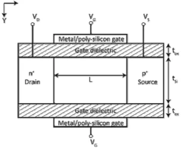
The Tunnel Field Effect Transistors (TFET) is identified as a reverse-biased p-i-n structure. Unlike the current in a conventional MOSFET it is not based on thermionic emission of carriers but the tunneling of these carriers through a potential barrier. The tunneling probability is high when the tunnel barrier is thin and the difference in the potential barrier height and the particle energy is small. As a result, keeping the power consumption within an acceptable limit is easily achieved feasible. The TFETs, due to their different mechanism of current transport from MOSFET exhibit several interesting electrical characteristics such as the potential for lowering the 60mV/decade subthreshold swing, ultra-low power consumption, ultra-low voltage operation, better short-channel performance, reduction in the leakage currents, exceeding the speed requirements due to tunneling effects, ability to work on sub-threshold and super-threshold voltage with similarity in fabrication process as compared to MOSFET and higher IOFF/ION current ratio. In this work, we choose a (DG-TFET) structure, as shown in Fig. 1. The list of parameters used is given in Table 1. This paper has been organized as follows. In section 2, the working principles and device physics of DG-TFET is presented. The simulation results are discussed in section 3. Finally, the conclusion is presented in section 4.
*Corresponding author: [email protected] 2000 UTHM Publisher. All right reserved.
Elgamal et al., Int. J. of Integrated Engineering Vol. 11 No. 7 (2019) p. 40-46
41
Fig. 1 - The Conventional TFET
Table 1 - The device parameters
The device parameter Value/Range Source Doping (NA) 1×10²⁰atoms/ cm3
Drain Doping (ND) 5×10¹⁸, 1×10¹⁹, 5×10¹⁹atoms/ cm3
Channel Doping (NAor ND) 1×10¹⁷atoms/ cm3
Source Length 60 nm
Drain Length 60 nm
Channel Length (L) 50 nm
Gate Oxide Thickness (tox) 3 nm
Silicon Body Thickness (tSi) 10 nm
Gate Work Function (Φm) 3.8 eV~4.5 eV
2. Working principles and device physics
The work mechanism of a TFET is based on band-to-band tunneling. BTBT employs tunneling of carriers from the valence band into the conduction band through the forbidden bandgap or vice versa. Generating current in both the on and off state which are the Ion where the VGS > VT and IOFF where VGS < VT. IOFF has Ithermalthat decreases by
increasing the bandgap of the TFET material. As the gate voltage increase the drain current increases which is quantified by the subthreshold swing.
The subthreshold swing is defined as the change required for increasing the drain current by a factor of 10 in the gate voltage. A low subthreshold swing is always targeted, for low power consumption by gate voltage that controls the on current. As for the other on region responsible the threshold voltage which can be controlled by the work function of the gate material. The threshold voltage has a linear relationship with the work function of the gate [3]. The threshold voltage is defined as the gate voltage at which the drain current reaches 1 × 10⁻⁷ A at VDS equal to the supply voltage which is taken to be one volt.
The work function of the gate controls the height of the potential barrier which predominate the electrons energy making the tunneling probability that is calculated by Eq. (1) decrease. Another factor that controls the probability of tunneling is the width of the barrier which is controlled by the doping whether it was doped with acceptors or donors to provide available states in addition to the width of the channel exponentially related to the tunneling probability. If the tunneling width is decreased, the tunneling probability increases exponentially [3].
(1)
Ptis the probability of tunneling,Fis the electric field,mis the mass of the particle, and is the Planck constant, (U0−
temperature-dependent band parameters.
3. Results and discussion
Data sets were generated from Silvaco simulator and then analyzed via MATLAB to extract different parameters such as on current, ambipolar current, subthreshold swing and on/off ratio. Besides, other parameters that were used to understand these parameters. In addition to comparing them and generating the following graphs.
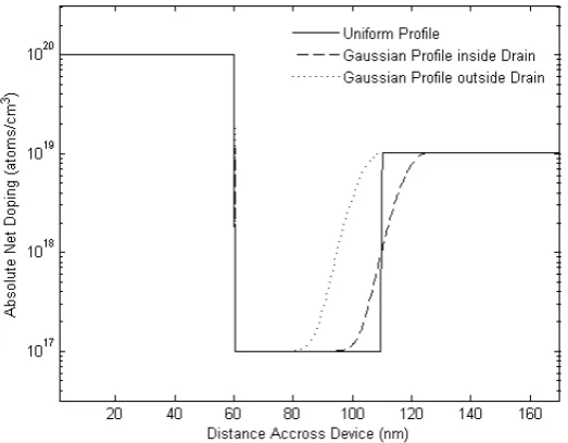
The use of different doping concentrations 5× 10¹⁸ atoms/cm3and 1×10¹⁹ atoms/cm3will be studied in different
doping profiles as these shown in Fig. 2. Specifically, the uniform doping profile, Gaussian profile terminating within the 60-nm drain, and other Gaussian profile terminating deeper in the channel will be studied as doping profiles. The performance of the device will be investigated through the change of work function of the both gates [3].
Fig. 2 - Doping profile for drain doping of 1×10¹⁹atoms/cm3
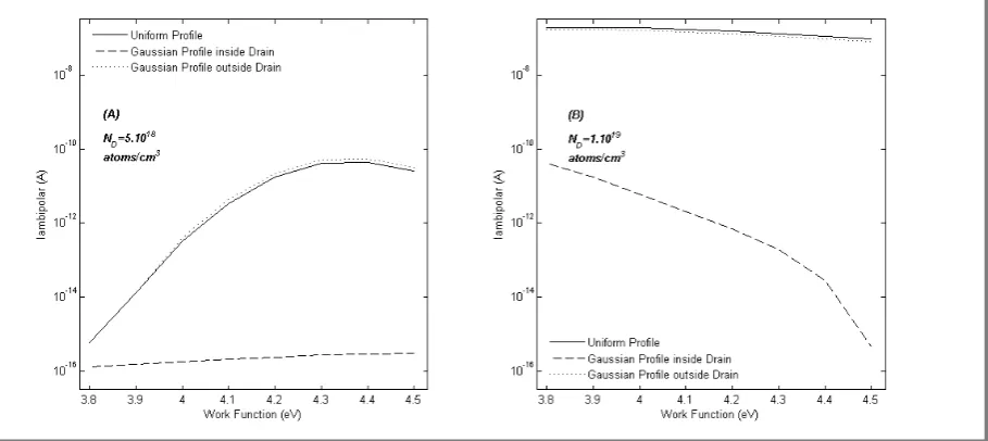
Fig. 3 - The on current in different doping concentrations with the work function
Fig. 3(A) display the on current in logarithmic scale in the doping of 5e×18 atoms/cm3. The three doping profiles are
Elgamal et al., Int. J. of Integrated Engineering Vol. 11 No. 7 (2019) p. 40-46
43
concentration but it decreases drastically at work function of 4.4 eV. The on current is a result of the BTBT from source to channel which gets effected by the barrier height which is controlled by the work function. While the doping concentration controls the allowed states for the current. When using the Gaussian doping; the depletion width between channel and drain junction increases lowering the tunneling probability causing a decrease in on current. It is for the current. When using the Gaussian doping; the depletion width between channel and drain junction increases lowering the tunneling probability causing a decrease in on current.
Fig. 4(A) the first concentration of 5×10¹⁸ atoms/ cm3 shows how the uniform and Gaussian out-drain doping
ambipolar current have the same value of 1e-15 mA and increases with the increasing of the work function and decreases after it reaches 4.4 work function, while the in-drain Gaussian doped increases insignificantly linearly with the work function. The second graph in Fig. 4(B) shows the doping of 1×10¹⁹atoms/cm3has the same effect where the
out-drain Gaussian doped and the uniformly doped has the same value of 1e-6 mA while the in-drain Gaussian doped has a value of 1e-10 then keeps decreasing with the increase of the work function. The band to band tunneling in the drain–channel junction is minimized in a TFET by reducing the drain doping that’s why the lowest value of the ambipolar current is at the lowest doping concentration [4]. The height of the barrier is controlled by the work function of the metal and the nature of the metal– semiconductor interface. And by increasing the work function the barrier increases making the BTBT from drain to channel harder.
Fig. 4 - The figures above displays the ambipolar current and work function in different doping
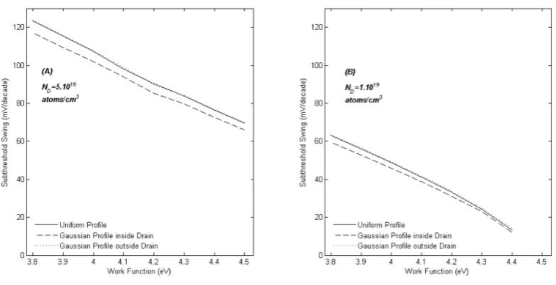
At Fig. 5(A) the subthreshold swing in linear scale. In the first doping of 5×10¹⁸atoms/ cm3the uniform, Gaussian
in- drain and Gaussian out-drain distributions has almost a SS value near 100 mv/decade. In Fig. 5(B) the second doping of 1×10¹⁹atoms/cm3gives the lowest SS of decreasing value from 60 mV/decade until the work function of 4.4.
The average SS of symmetric TFET as in Eq. (2),
(2)
where Vonis taken to be one volt and Voffis the voltage where the current starts to increase [4,5]. The off-current Ioffis
defined as the drain current when gate voltage is Voffand is the drain current at one volt. The subthreshold voltage
decreases linearly while increasing the work function, as the whole IV curve shifts toward right as Voff increases,
lowIOFF. The Gaussian out-drain and uniform distributions has the value of 1×10 then all decrease for the decreasing
of the on current at concentration of 5×10¹⁸atoms/cm3. In Fig. 6(B) that represents the 1×10¹⁹atoms/ cm3doping where
the in-drain Gaussian doped has the highest value of 1×10¹⁰while the uniformly doped drain and Gaussian doped
out-drain has the same value of 1×10¹¹ the decreases abruptly after the work function of 4.4. This sudden decrease is
accounted to the way the ON current is defined as the current at one volt, which decreases due to the increase of the gate work function which shifts the whole transfer characteristics to the right. So as the ON current is decreased and the ON/OFF ratio dropped accordingly. Taking in consideration the drain doping increase, which affects more the ON current, the effect of characteristics shift becomes more apparent. When using Gaussian doping the off current decreases causing a higherIon/IOFFratio while the increase of the work function will affect the BTBT in source, so the
ratio decreases. After comparing the values, we found that the device that functions at a doping of 5×10¹⁸and a work
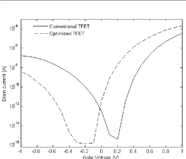
function of 4.2 is optimum. And compering that to the conventional TFET shown in Fig. 7.
Elgamal et al., Int. J. of Integrated Engineering Vol. 11 No. 7 (2019) p. 40-46
45
Table 2 - Conventional vs. optimum device
The device parameter Conventional device Optimized device
Source Doping (NA) Uniform Gaussian
Drain Doping (ND) 1×10²⁰atoms/ cm3 1×10²⁰atoms/ cm3
Channel Doping (NAor ND) 1×10¹⁹atoms/ cm3 5×10¹⁸atoms/ cm3
Source Length 1×10¹⁷atoms/ cm3 1×10¹⁷atoms/ cm3
Drain Length 50 nm 50 nm
Channel Length (L) 3 nm 3 nm
Gate Oxide Thickness (tox) 10 nm 10 nm
Silicon Body Thickness (tSi) 4.5 eV 4.2 eV
Gate Work Function (Φm) Uniform Gaussian inside Drain
Fig. 7 - Conventional and optimized TFET I-V characteristics
4. Conclusion
In this paper, the effect of the gate work function and the doping profile terminating within and outside the drain has been studied. It observed that the optimum characteristics can be achieved with the doping concentration of 5x1018cm-3
and gate work function of 4.2 eV with Gaussian profile inside the drain. Moreover, it observed that when the work function increased from 3.8 eV To 4.5 eV the Ion/ Ioffdecreased from 9.17x10¹²to 2.5x10¹², and the subthreshold swing
changed from 117.1 mV/decade to 66 mV/decade mV/decade with Gaussian profile inside the drain.
References
[1] ZA, N.F., Ahmad, I., Ker, P.J. and Menon, P.S., 2015. Modelling and Characterization of a 14 nm Planar p-Type MOSFET Device. International Journal of Integrated Engineering,7(3).
Applied Engineering Research, 11(7), 4922-4929.
[5] Ramaswamy, S., & Kumar, M. J. (2017). Double gate symmetric tunnel FET: investigation and analysis. IET Circuits, Devices & Systems, 11(4), 365–370.
[6] Choi, W. Y., Park, B. G., Lee, J. D., & Liu, T. J. K. (2007). Tunneling Field-Effect Transistors (TFETs) With Subthreshold Swing (SS) Less Than 60 mV/dec. IEEE Electron Device Letters, 28(8), 743–745.
[7] Cao, W., Sarkar, D., Khatami, Y., Kang, J., & Banerjee, K. (2014). Subthreshold-swing physics of tunnel field-effect transistors. AIP Advances, 4(6) 067141.
[8] Chen, Y. N., Chen, C.J., Fan, M. L., Hu, V., Su, P., & Chuang, C. T. (2015). Impacts of Work Function Variation and Line-Edge Roughness on TFET and FinFET Devices and 32-Bit CLA Circuits. Journal of Low Power Electronics and Applications, 5(2), 101–115.
[9]Elgamal, Muhammad, and Mostafa Fedawy. "Optimizing Gate-on-Source Overlapped TFET Device Parameters by Changing Gate Differential Work Function and Overlap Dielectric."2019 International Conference on Innovative Trends in Computer Engineering (ITCE). IEEE, 2019.
[10] Elnaggar, Mohamed, Ahmed Shaker, and Mostafa Fedawy. A comprehensive investigation of TFETs with semiconducting silicide source: impact of gate drain underlap and interface traps.Semiconductor Science and Technology 34.4 (2019): 045015. [11] Elnaggar, Mohamed, Ahmed Shaker, and Mostafa Fedawy. "Modified Hetero-Gate-Dielectric TFET for Improved Analog and