Temperature Independent Band Gap
Reference Voltage Using Regulated
Cascode Current Mirror Structure
N.Divya Teja#1
#1 B.Tech Project Student, Department of ECE, KL University, Vaddeswaram, Guntur-522502
K.Shreeram#2
#2 B.Tech Project Student, Department of ECE, KL University, Vaddeswaram, Guntur-522502
G.Rakesh chowdary#3, Ch.Srinath Babu#4, K.Sneha latha#5
#3 Assistant professor, Department of ECE, KLUniversity, Vaddeswaram, Guntur-522502
#4,#5 B.Tech Project Students, Department of ECE, KL University, Vaddeswaram, Guntur-522502
Abstract:
A bandgap reference is a temperature independent voltage reference circuit widely used in integrated circuits usually with an output voltage of 1.25V, close to the theoretical 1.22eV bandgap of silicon at 0k. It is the essential component of an analog-to-digital converter. There are some problems arising from temperature-dependent to power supply rejection ratio when implementing a bandgap reference circuit. The circuit uses a regulated cascade current mirror structure which is the best suitable current mirror for the bandgap reference circuit as it provides medium input and output compliance voltage and very high output resistance. The main design criteria for this project is to achieve PSRR above 60dB and a variation less than 3% resulting from temperature changes between 27ºC and 85ºC.
Keywords ---bandgap, PSRR, reference voltage, regulated cascade current mirror.
1. Introduction
The bandgap reference circuit concept was first published by David Hilbiber in 1964[1]. Bob widlar[2], Paul Browkaw[3] and others[4] followed up with other commercially successful versions. Bandgap circuit with low sensitivity to temperature and supply voltage is commonly required. The best approach is the base emitter junction which consists of a linear combination of base-emitter voltage. We can compensate temperature dependent voltage by adding a positive-TC voltage to a negative-TC voltage. The temperature behavior of a pn junction voltage is described by
= ln – – VT
where VT is the thermal voltage. With T at room temperature and VBE=750mv,
≈ -1.5mv/ºK
The positive-TC voltage comes from the voltage difference between two pn junctions. The fig. 2 shows the reason behind positive-TC voltage.
= VT ln n
where n equals to the current density ratio of Q2 to Q1.
Ideally, adding a positive-TC voltage to a negative-TC voltage can realize a zero temperature coefficient 1.26V at the room temperature. Additionally, the reference voltage is required to be robust to the power supply voltage. An easy way to improve power supply rejection ration (PSRR) is to increase the open loop gain.
2. Temperature Independent References
[5]
Reference voltages or currents that exhibit little dependence on temperature prove essential in many analog circuits. It is interesting to note that, since most process parameters vary with temperature, if a reference is temperature-independent, then it is usually process- independent as well.
We postulate that if two quantities having opposite temperature coefficients’ (TCs) are added with proper weighting, the result displays a zero TC. Among various device parameters in semiconductor technologies, the characteristics of bipolar transistors have proven the most reproducible and well-defined quantities that can provide positive and negative TCs. Even though many parameters of MOS devices have been considered for the task of reference generation, bipolar operation still forms the core of such circuits.
2.1 Negative TC-Voltage
The base-emitter voltage of bipolar transistors or, more generally, the forward voltage of a pn junction diode exhibits a negative TC. For a bipolar device we can write
IC=IS exp(VBE/VT), where VT=kT/q……...(1)
The saturation currents IS α µkTni2, where µ denotes the mobility of minority carriers and ni is the intrinsic
minority carrier concentration of silicon. The temperature dependence of the quantities is represented as µ α µoTm, where m ≈ -3/2, and ni2α T3 exp[-Eg/(kT)], where Eg≈1.12eV is the bandgap energy of silicon. Thus,
IS=bT(4+m)exp(-Eg/kT)………...…(2)
where b is a proportionality factor. Writing VBE=VTln(IC/IS), we can now compute the TC of base-emitter
voltage. In taking the derivative of VBE with respect to T, we must know the behavior of IC as a function of
temperature. To simplify the analysis, we assume for now that IC is held constant. Thus,
= * ln( ) – * ………..….(3)
From equation (2)
= b(4+m)T(3+m) exp(-Eg/kT) + bT(4+m) exp(-Eg/kT) (Eg/Kt2)………(4)
Therefore,
* = (4+m) + (Eg/kT2) * VT…………(5)
With the aid equations (4) and (5), we can write
From the above equation, we note that the temperature coefficient of VBE itself depends on the
temperature, creating error in constant reference generation if the positive-TC quantity exhibit a constant temperature coefficient.
B. Positive TC-Voltage
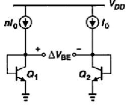
It was recognized in 1964 that if two bipolar transistors operate at unequal current densities, then the difference between their base-emitter voltages is directly proportional to the absolute temperature.
Figure 1 Generation of PTAT voltage
Ligible, then
∆VBE = VBE1 – VBE2
= VT ln – VT ln = VT ln n.
Thus the VBE difference exhibits a positive temperature coefficient:
= ln n
This TC is independent of the temperature or behavior of the collector currents.
3. Circuit Operation Of BGR
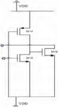
3.1 Start Up Circuit
Fig 2 Start Up Circuit
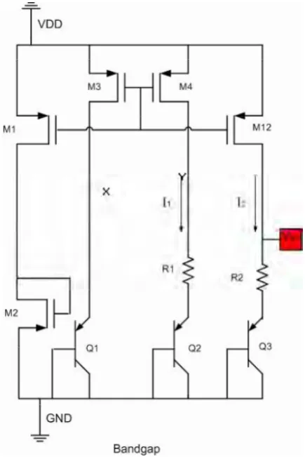
3.2 Differential Amplifier
In the circuit depicted in Fig 3, we need to force node X and Y to have the same voltage. We use an operational amplifier for this purpose. It is composed by the common-source stages with diode-connected loads. In order to increase the gain, we stack two pmos transistors into it and its gain can be expressed as
AV = gm10 [(gm8 + gmb8)ro6r08 //ro10]
Its output provides a bias for the entire circuits, and a feedback loop is formed. Therefore[7], this bias voltage ideally provides a constant Vgs for the pmos transistors and a constant current can be obtained.
Figure 4 Basic bandgap circuit
VX = VY = VBE1 = VBE2 + I1×R1 where
VBE = VT ln ( )
Therefore,
VBE1 – VBE2 = VT ln n = I1×R1
The voltage difference between the two pn junctions is the positive-TC voltage. The current across R1 equals to VT hich is called the proportional to absolute temperature (PTAT) current. A PTAT current can be
copied from the current mirror and can be adjusted by changing the width of M12 or the resistance of R1. Adding a positive-TC voltage I2R2 to a base-emitter voltage, the negative-TC voltage, can achieve a temperature
independent voltage. The ideally reference voltage equals
Vref = VBE3 + VT R2
The n is usually chosen to be eight for the layout purpose.
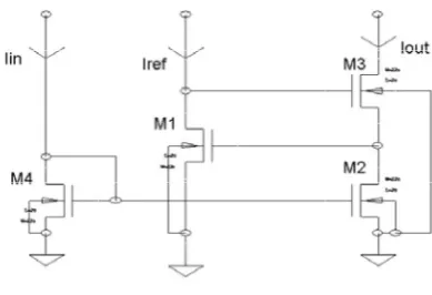
4. Regulated Cascode CM Structure
Figure 5 Regulated Cascode CM
The output compliance voltage for this structure is given as
Vout = +
The output resistance for this structure is given as
rout≈ rds2gm3rds3gm1rds1
So this structure achieves an output resistance on the order of gm2rds3
The output characteristic of this structure is shown in Fig. 6
Figure 6 Output characteristics for Regulated Cascode CM
As can be seen from the above Fig 6, output compliance voltage for this structure is 1.5V. Also in saturation mode, output current is constant as it should be ideally.
5. Simulation
The reference voltage is required to be 1.26V at room temperature. The relationship between reference voltage and base-emitter voltage is given by
Vref = VBE3 + I2R2
The base-emitter voltage is 0.75V at 25ºC. We can set the PTAT current going through R2 to be 54µA.
Therefore, from the above equation, the resistance of R2 can be determined by
≈ 9.4K
For Cadence[11] simulation, the appropriate R2 is 9.37K. Fig. 6 shows the reference voltage changes with temperature ranging from 27ºC to 85ºC and 10% supply voltage variation. The reference voltage changes around 7.24mV The Vref is very low sensitive to the changes of the temperature. The power supply rejection
The power supply rejection ratio is shown in Fig 7 and from the figure, it is clear that the circuit of the BGR is robust to the power supply when the temperature changes from 27ºC to 56ºC. The exact PSRR and reference voltages for certain values are depicted in the Table 1.
Table 1 Outcomes of PSRR and reference voltage at certain temperature.
Temperature(ºC) Voltage Variation
27ºC 376.707µV
55.6 ºC 499.067µV
85 ºC 1.25189mV
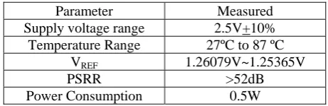
6. Conclusion
A design using bandgap core circuit with Op amp and start-up circuit is presented and simulated. The overall performance of the bandgap reference circuit is summarized in the table 2.
Table 2 Summary of performance
Parameter Measured
Supply voltage range 2.5V+10%
Temperature Range 27ºC to 87 ºC
VREF 1.26079V~1.25365V
PSRR >52dB
Power Consumption 0.5W
Comparisons with other design are shown in table 3.
Table 3(a) Comparison between different designs
Design[12] Our Design
Supply Voltage 1V 2.5V
PSRR >40dB >60dB Temperature
Variation
1.2mV~5.4Mv (-20 ºC~50ºC)
7mV≈0.58% (27ºC~85ºC)
Table 3(b) Comparison between different designs
Design[13] Our Design
Supply Voltage 2V 2.5V
Temperature Variation
<0.1% (-30ºC~125ºC)
7mV≈0.58% (27ºC~85ºC) Power
Consumption
2.2mW 0.5mW
Acknowledgments
References
[1] Hilbiber, D.F. (1964), "A new semiconductor voltage standard", 1964 International Solid-State Circuits Conference: Digest of Technical Papers2:32-33.
[2] Widlar, Robert J. (February 1971), "New Developments in IC Voltage Regualtors", IEEE Journal of Solid-State Circuits 6 (1): 2–7. [3] Brokaw, Paul (December 1974), "A simple three-terminal IC bandgap reference", IEEE Journal of Solid-State Circuits 9 (6): 388–
393.
[4] Banba, H.; Shiga, H.; Umezawa, A.; Miyaba, T.; Tanzawa, T.; Atsumi, S.; Sakui, K. (May 1999), "A CMOS bandgap reference circuit with sub-1-V operation", IEEE Journal of Solid-State Circuits34 (5): 670–674.
[5] David jones “Analog Integrated Circuit Design.
[6] K. Lasanen, V. Korkala, “Design of a 1-V low power CMOS bandgap reference based on resistive subdivision”, IEEE.
[7] T. L. Brooks and A. L. Westwick, “A low-power differential CMOS bandgap reference,” in ISSCC Dig. Tech. Papers, Feb. 1994, pp. 248–249.
[8] Behzad Razavi, “ Design of Analog CMOS Integrated Circuits”, McGRAW-Hill, 2000.
[9] M. Ismail and T. Fiez, “Analog VLSI Signal and Information Processing,” New York: Tata McGraw-Hill 2002. [10] P.E. Allen and D. R. Holberg, “CMOS analog circuit design,” New York: Oxford University Press, 2002.
[11] S. S. Rajput and S. S. Janmuar, “A high performance current mirror for low voltage designs,” Proc. APCCAS-2000/IEEE, Tianjin pp. 170-173, China, Dec 2000.
[12] I. M. Filanovsky, “Current Mirrors with Limiting of Linear Dynamic Range,” University of Alberta, Edmonton, Alberta, Canada, T6G 2E1.
[13] E. SACKINGER and W.GUGGENBUHL, “A versatile building block: the CMOS differential difference amplifier,” IEEE SC-22, (2), PP. 287-294.
[14] D. A. Johns and K. Martin, “Analog Integrated Circuit Design,” John Wiley & Sons, Inc., New York, 1997.
[15] G. R. Wilson, “A Monolithic Junction FET-npn Operational Amplifier,” IEEE J. Solid-State Circuits, Vol. SC-3, No. 5, pp.341-348, Dec. 1968.