ANALYSIS AND MITIGATION OF
COMMON MODE AND DIFFERENTIAL
MODE NOISE ON BOOST CONVERTERS
C.Krishna Kumar
Assistant Professor (ss), Department of EEE, Periyar Maniammai University. Thanjavur- 613403.
Dr.A.Nirmal Kumar
Head of Electrical Engineering, Bannariamman Institute of Technology. Sathyamangalam.
Dr. B.Karthikeyan
Associate Professor, BITS Dubai campus. Dubai
Ms.R.Abinaya
Research Scholar, Periyar Maniammai University, Thanjavur-613403.
ABSTRACT
This paper is about the study and analysis on the effects of snubber circuits such as RLD, RCD and mixed (RLD+RCD) over the conducted ELECTROMAGNETIC INTERFERENCE on high frequency power MOSFET. In this paper for various duty cycles separation of conducted EMI is done with the help of LISN circuit. The analysis is done for various duty cycles as 0.5, 0.55 and 0.6 for a switching frequency of 50 KHz using ORCAD PSPICE software. The simulated results are then compared with respect to their duty cycle.
KEYWORDS
Electromagnetic Interference (EMI), Line Impedance Stabilization Network (LISN), Differential Mode, Common mode.
I. INTRODUCTION
DC to DC converter is an electronic circuit which converts a source of direct current (DC) from one voltage level to another.
It is a class of power converter. DC to DC converters are important in portable electronic devices such as cellular phones and laptop computers, which are supplied with power from batteries primarily. This conversion can be done by two methods. They are: (i) LINEAR
conversion and (ii) SWITCH MODE conversion.
Linear output can give output at lower voltages only. They are inefficient when the voltage drop is large and the current is high as they dissipate power as heat which is equal to the product of voltage and current. This inefficiency wastes power and require high rated, expensive and larger components.[1]-[2]
Electronic switch mode DC-DC converter converts one level of voltage to another by storing the input energy temporarily and releasing that energy to the output at different voltages. The energy can be either stored in magnetic field storage (inductor) or electric field storage (capacitor) components.
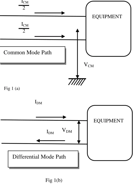
Conducted EMI occurs due the physical contact of the conductors due to induction in the frequency range of 9 KHz to 30 MHz. This is of two types. They are: (i) Common mode noise and (ii) Differential mode noise.
The noise is actually produced at the time of high dv/dt & di/dt switching operations. High rates of dv/dt and parasitic capacitor are the main sources of common mode interference. During turn on period di/dt may rise to a higher value and during turn of period dv/dt may rise to a higher value [2].
Fig 1 (a)
Fig 1(b) Fig 1(a): common mode path (b): differential mode path
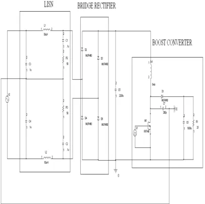
1) LISN CIRCUIT
The different noises can be separated by using a LISN (Line Impedance Stabilization Network)[8]. This circuit consists of inductors, capacitors and resistors. The inductor and capacitor are for filtering the noise and the inductor also separates the unwanted high frequency noises.
EQUIPMENT
Common Mode Path ICM
2
ICM
2
VCM
EQUIPMENT
Differential Mode Path VDM
IDM
Fig 1( c). LISN CIRCUIT
2) SNUBBER CIRCUIT
Snubber circuits are the essential parts of the power electronics. Snubber circuits can reduce the di/dt and dv/dt during turn on and turn off period respectively. The snubber circuits are of two types. They are active snubber and passive snubber circuits [4]. Mostly the passive snubbers are used in practice. Because an extra switch is required for active snubbers, thereby increasing the power loss. The snubber circuits are implemented for reducing the average power dissipation.
The main functions of snubber circuits are: Reducing the voltage and current spikes Reducing the average power dissipation. Limiting the dv/dt and di/dt levels.
RLD, RCD and mixed (RLD+RCD) circuits are taken for analysis.
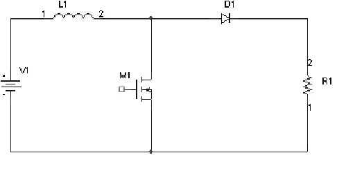
3) BOOST CONVERTER
A boost converter (step-up converter) is a power converter with an output DC voltage greater than its input DC voltage. It is a class of switching-mode power supply (SMPS) containing at least two semiconductor switches (a diode and a transistor) and at least one energy storage element. Filters made of capacitors (sometimes in combination with inductors) are normally added to the output of the converter to reduce output voltage ripple.
Fig 2. Boost converter
The output voltage of this converter will be more than the input and is equal to Vo=Vin/(1-D) where D is the duty ratio. It is defined as the ratio of on time to the total time period.
Fig 3(a): boost converter circuit without snubber
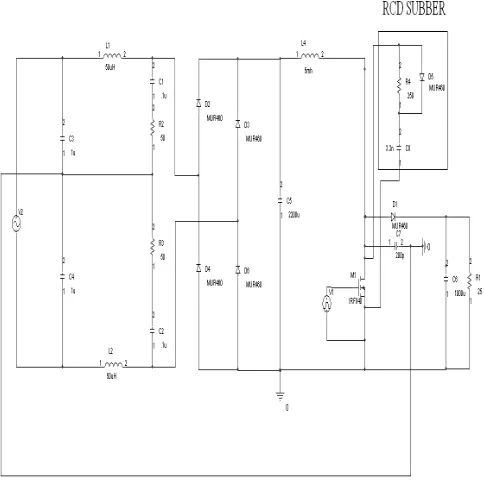
Fig 3(c): boost converter circuit with RCD snubber
The description of the circuits is as follows: Power MOSFET: IRF 840
DIODE: MUR 460 Starting time: 0 ms Run to time: 50 ms Step size: 0.05 us CIRCUIT DETAILS:
Cmain:2200uf;Lmain:5mH; Ls(RLD)=10uH; Rs(RLD)=50 ohm; R(RCD)= 250 ohm; C(RCD)=3.3 nF; C heat sink=220 pF;
Simulation is made for the above circuits with these specifications for different duty cycles between 0.5, 0.55 and 0.6. The analysis done on conducted noise is taken in the range of 9 KHz to 30 MHz [13].
TABLE 1: Boost converter without snubber
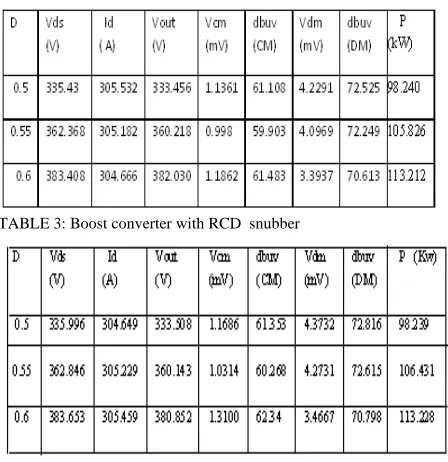
TABLE 3: Boost converter with RCD snubber
TABLE 4: Boost converter with RLD+RCD snubber
The results shown above are the peak values of voltage drop across the power MOSFET (Vds), drain current (Id), output voltage (Vo), magnitude of common mode noise (Vcm) and magnitude of differential mode noise (Vdm). The separation of common mode and differential mode conducted EMI was done using LISN circuit and by using PSPICE software. The magnitude of the voltage noise can be found out with the following formula [6]
db uv=20*log10 (Vnoise (mV)/1uV)
In RLD+RCD snubber circuit the mitigation of noise level is good when compared to RLD and RCD snubber circuits.
0 0.5 1 1.5 2 2.5 x 10⁷ -100 -80 -60 -40 -20 0 20 40 60 80 100 frequency n oi s e dbuv
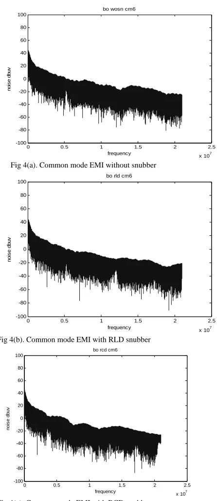
bo wosn cm6
Fig 4(a). Common mode EMI without snubber
0 0.5 1 1.5 2 2.5
x 107 -100 -80 -60 -40 -20 0 20 40 60 80 100 frequency noi s e dbuv
bo rld cm6
Fig 4(b). Common mode EMI with RLD snubber
0 0.5 1 1.5 2 2.5
x 107 -100 -80 -60 -40 -20 0 20 40 60 80 100 frequency no is e dbuv
bo rcd cm6
0 0.5 1 1.5 2 2.5 x 10⁷ -100 -80 -60 -40 -20 0 20 40 60 80 100 frequency bo rldrcd cm6
no
is
e
db
uv
Fig 4(d) Common mode EMI with RLD+RCD snubber
0 0.5 1 1.5 2 2.5
x 107 -80 -60 -40 -20 0 20 40 60 80 100 120 frequency nois e dbuv
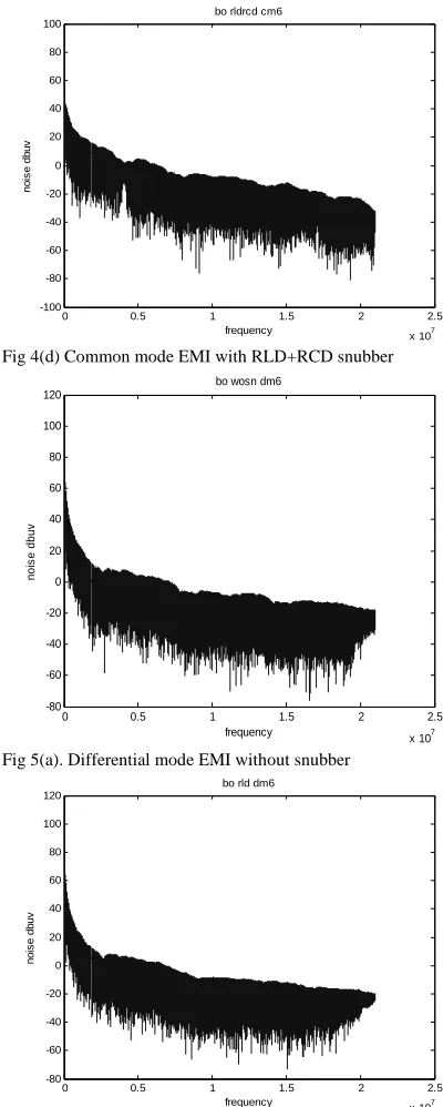
bo wosn dm6
Fig 5(a). Differential mode EMI without snubber
0 0.5 1 1.5 2 2.5
x 107 -80 -60 -40 -20 0 20 40 60 80 100 120 frequency no is e db uv
bo rld dm6
0 0.5 1 1.5 2 2.5 x 10⁷ -80 -60 -40 -20 0 20 40 60 80 100 120 frequency no is e db uv
bo rcd dm6
Fig 5(c). Differential mode EMI with RCD snubber
0 0.5 1 1.5 2 2.5
x 107 -80 -60 -40 -20 0 20 40 60 80 100 120 frequency n oi s e d buv
bo rld+rcd dm6
Fig 5(d). Differential mode EMI with RLD+RCD snubber
6) COMPARISON WAVEFORMS FOR DUTY CYCLE D=0.6
Common mode:
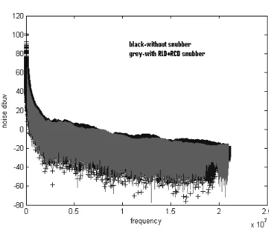
Fig6 (b). Comparison of with and without RLD snubber
Fig6(c). Comparison of with and without RLD+RCD snubber
Differential mode:
Fig7 (b). Comparison of with and without RLD snubber
Fig7(c). Comparison of with and without RLD+RCD snubber
WAVE FORMS OF DRAIN CURRENT, DROP ACROSS THE SWITCH AND POWER LOSS: BOOST CONVERTER WITHOUT SNUBBER:
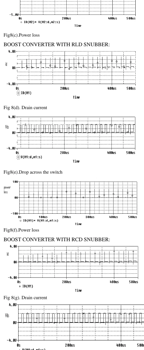
Fig8(c).Power loss
BOOST CONVERTER WITH RLD SNUBBER:
Fig 8(d). Drain current
Fig8(e).Drop across the switch
Fig8(f).Power loss
BOOST CONVERTER WITH RCD SNUBBER:
Fig8(i).Power loss
BOOST CONVERTER WITH RLD+RCD SNUBBER:
Fig 8(j). Drain current
Fig8(k).Drop across the switch
From fig 7(a), the conducted EMI gets reduced up to 20 db, 3 db, 12 db and 15 db in the frequency range of 9 KHz to 1MH, 1MHz to 5MHz, 5MHzto 7MHz and 17MHz to 21MHz respectively. From fig 7(b), the conducted EMI gets reduced up to 20 db, 5 db, 8 db and 15 db in the frequency range of 9 KHz to 1MHz, 1MHz to 8MHz and 8MHz to 15MHz and 17MHz to 21MHz respectively. From fig 7(c), the conducted EMI gets reduced up to 20 db, 7 db and 25 db in the frequency range of 9 KHz to 1MH, 15MHz to 17MHz and 17MHz to 20MHz respectively and 5 db in the frequency range of 1MHz to 7MHz and 9MHz to 15MHz.
From these, it is observed that RLD+RCD snubber is working better than other two snubber circuits. The power loss produced by the RLD+RCD snubber is low compared to other snubber circuits refer fig 9(d). After RLD+RCD the power loss produced by RLD snubber is low. Here the reference noise level taken is 0 db.These snubbers reduce the noise level by bringing the noise magnitude nearer to 0 db. Through the overall analysis RLD+RCD snubber is better at lower frequencies in the range of 9 KHz to 5MHz. Fig 9(e) and 9(f) shows that RLC is better than RCD and RLD+RCD is better than RLD snubber respectively.
7) CONCLUSION
This paper aimed at simulation and comparison of the boost converter without any snubber circuits, with RLD, RCD and RLD+RCD snubber circuits for different duty cycles. The EMI was analyzed in the range of 9 KHz to 30 MHz The main cause for this EMI in this circuit is due to the high switching frequency of power MOSFET. This was reduced by using passive snubber circuits such as RLD, RCD and RLD+RCD snubbers. The following are found through this analysis:
It was found that with these snubber circuits the voltage and current spikes can be reduced in buck converters. It was found that the power loss was also reduced with these snubber circuits.
With RLD+RCD snubber circuit there is a considerable reduction in the noise level at the frequency of 5 MHz With RLD snubber circuit there is no much reduction in the noise level. There is only a slight change after the frequency of 3 MHz
REFERENCES
[1] B.W Williams, Power Electronics Devices, Drives and Application, MacMillan Education Ltd. London.1987.
[2] N. Mohan, T.M. Undeland and W.P. Pobbons, “Power Electronics Converters Applications and Design”, Second edition, John Wiley and
Sons: Singapore, Inc. 1995.
[3] W. McMurray, “Selection of Snubbers and clams to optimize their design of transistor switching converters”. IEEE
trans.Ind.Appl.,Vol.[A-16.pp.513-523,July/Aug,1980.
[4] M.H. Rashid. “Spice for Power Electronics and Electric Power”. Prentice Hall, Englewood Cliffs, New Jersey 1993.
[5] Oto Tezak,Drago Dolinor,and Miro Milanovie, “ Snubber Design Approach for DC-DC Converter Based on Differential Evolution
Method” IEEE Conference AMC 2004, pp 87-91. Kawasaki, Japan.
[6] Shao j., Lin, R.L., Lee, F.C. and Chan, D.Y. “Characterization of EMI Performance for Hard and Soft Switched Inverters”. Applied Power
Electronics Conference and Exposition.2000 APEC2000. Fifteenth Annual IEEE Vol.2, 2000 pp. 1009-1014
[7] W.Teulings, et al., A new technique for spectral analysis of conducted noise of a SMPS including interconnects, proceedings of IEEE PESC
1997, pp. 1516-1521.
[8] S.Kaitwanidvilai,K.unchaleevara pan, B. Hutawarakornand Y. Prempraneerach, “The Effect of Switching Frequency and duty cycle on
SMPC Conducted Emission: Simulation and Experimental”, IPEC '99 Conference Proceedings 1999, vol. 1,pp. 667- 672.
[9] Kenichiro Fujiwara and Hiroshi Nomura, “A Novel Lossless Passive Snubber for Soft-Switching Boost-Type Converter”,IEEE Trans.
Power Electronics , vol. 14, no.6, 1999,pp.1065- 1069.
[10] H.P. Yee, “An EMI Suppression MOSFET Driver”, Applied Power Electronics Conference and Exposition, APEC '97 Conference
Proceedings 1997, 12th Annual, 1997, vol.1,pp. 242-248.
[11] W.Khan-ngern “Electromagnetic Compatability Experimental Laboratory on Power Electronics” ICEMC 2002/Bangkok 406-411.
[12] John C. Fluke, Sr, “Controlling Conducted Emissions by Design,” Van Nostrand Reinhold,1991,pp.49-63.
[13] C. U-Yaisom, V.Tarateeraseth,W.Khan-ngern, S. Nitta” The Analysis of Mixed Series and Parallel Snubbers to reduce Conducted EMI
Emission on a Switching Converter”IEEE conference.
[14] Kenichiro Fujiwara and Hiroshi Nomura, “ A Novel Lossless Passive Snubber for Soft-Switching Boost-Type Converter” IEEE Trans.
Power Electronics, Vol. 14, no.6, 1999, pp.1065-1069.
[15] J.D Van Wyk, Fred C.Lee Power electronics technology- status and future, Proceedings of IEEE PESC 1999, pp 3-12.
[16] Shao j., Lin, R.L., Lee, F.C. and Chan, D.Y. “Characterization of EMI Performance for Hard and Soft Switched Inverters”. Applied Power
Electronics Conference and Exposition.2000 APEC2000. Fifteenth Annual IEEE Vol.2, 2000 pp. 1009-1014