397 |
P a g e
DESIGN AND IMPLEMENTATION OF A LOW
VOLTAGE LOW POWER DOUBLE TAIL
COMPARATOR
1
C.Hamsaveni,
2R.Ramya
1,2
PG Scholar,
Department of ECE, Hindusthan Institute of Technology, Coimbatore(India)
ABSTRACT
Comparators are the basic elements for designing the modern analog and mixed signal systems. The speed and
area is main factors for high speed applications. Various types of dynamic double tail comparators are compared in
terms of Delay, Area, Power, Glitches, Speed and average time. The accuracy of comparators it mainly defined by
its power consumption and speed. The comparators are mainly achieving the overall higher performance of ADC.
The High speed comparators suffer from low voltage supply. Threshold voltage of the device is not scaled at the
same time, as the supply voltage of the device. In modern CMOS technology the double tail comparator is designed
by a using the dynamic method, it mainly reduces the power and voltage. The analytical expression method it can
obtain an intuition about the contributors, comparator delay and explore the trade-off dynamic comparator design.
Keyword: Double Tail comparator, ADC, Dynamic comparator, Glitches
I INTRODUCTION
398 |
P a g e
voltages. However the supply voltage is lowered the performance of analogue circuits is degraded and the design of low voltage analogue Circuits
This technique is very suitable for very-low power clocked and continuous time circuits such as level shifters, Op-amp and comparators. Design of a 10-bit supply boosted (SB) SAR ADC is presented as an exOp-ample of the technique. Voltage design techniques such as clock boosting were also used. A unique supply and clock booster was designed as integral part of new supply boosted comparator. Input common mode range of SB comparator was extended by using supply boosted level shifter circuits [6]. Among the key performance metrics of a dynamic latch used in a voltage comparator is its input referred offset voltage. Relevant effects that contribute to the offset can be divided into static and dynamic components. The most commonly discussed source of static offset stems from threshold voltage mismatch in the constituent transistors. Two simple equations for predicting the offset were derived and compared against simulation data [7].
The degeneration resistors are the latching pair and it’s to reduce transistor charging time for regeneration. Charging
time, they allowing more time for regeneration. The introduction method consists of the emitter degeneration resistors in the latching pair. The degeneration resistors reduce the transistor charging time, providing more time for the critical process of regeneration. As the latching pair is isolated from the input nodes degenerates still improves the sensitivity when a preamplifier is used [8]. To overcome the challenges associated with to reduce the supply voltage, a double tail latched comparator with a variable capacitance, calibration technique they using a metal oxide metal capacitors is implemented. An all-digital time domain delay interpolation technique further enhances the resolution with very little additional power consumption [9].
II CONVENTIONAL DYNAMIC COMPARATOR
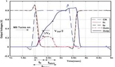
The double tail comparator achieves the better performance and the double tail comparator and the architecture it mainly used in the better performance used in the low voltage applications. The comparator designed based on double tail architecture. The main idea of this method is to increase ΔVfn/fp is to increase the latch regeneration speed. The main operation of the comparator is during reset phase CLK = 0, Mtail1 and Mtail2 is off, to avoiding these static power, M3 and M4 switches pulls both fn and fp nodes to VDD. Hence the transistor Mc1 and Mc2 are cut off, intermediate stage transistors MR1 and MR2 is reset both latches outputs to ground. During decision making phase CLK = VDD. Mtail1 and Mtail2 are on transistors M3 and M4 turn off. Furthermore, at the beginning of the phase, the control transistors are still off. Thus, fn and fp start to drop with different rates according to the input voltages. The second term, tlatch, is the latching delay of two cross coupled inverters. It is assumed that a voltage swing of Vout = VDD/2 has to be obtained from an initial output voltage difference V0 at the falling output. This is a self biasing differential amplifier. An inverter was added at the output of the amplifier as an additional gain stage, to isolate any load capacitance from the self biasing differential amplifier.
The size of M1 and M2 are set by considering the differential amplifier’s transconductance and the input
399 |
P a g e
comprises two main parts, t0 and tlatch. The delay t0 represents the capacitive charging of the load capacitance CL out (at the latch stage output nodes, Outn and Outp) until the first n-channel transistor (M9/M10) turns on, after which the latch regeneration starts; thus t0 is obtained where IB1 is the drain current of the M9 and approximately equal to the half of the tail current. Thus, it can be concluded that two main parameters which influence the initial output differential voltage and thereby the latch regeneration time are the transconductance of the intermediate stage transistors (gmR1,2) and the voltage difference at the first stage outputs (fn and fp) at time t0.
III PROPOSED DOUBLE TAIL COMPARATOR
To achieve the better performance of double tail architecture in low voltage applications, the proposed method comparator is designed based on the double-tail structure
Operation of Proposed Comparator
1.
Voltage is sense at the second stage input and the second stage latch regenerate output
voltage
Reset Phase: Clk = 0, Mtail1and Mtail2 OFF. For this process static power is avoided. np and nf nodes toVDD. Latches to be Ground.
2. Decision making phase: Clk = VDD, Mtail1 and Mtail2 are ON, M3 and M4 OFF.
During reset phase clk=0, Mtail1 (M3) &Mtail2 (M20) are OFF, M10&M13will pull both fn & fp nodes to VDD. Hence MC (M11) & MC (M12) are cut off, M6 M9 are discharge to output nodes to VSS. During an decision making phase clk =VDD,Mtail1(M3)&Mtail2(M20) are ON, transistor M10&M13 will OFF and fn & fp nodes are start drop with different rates according to input voltage. VINP>VINN means fn is faster than fp, M15 transistor provide more current thanM14.MC (M11) is turn on, fp node pulling back to VDD MC (M12) remains OFF, fn node discharged. Offset will low and delay reduced. Parallel connected dynamic latch is used as load of first stage to increase voltage difference due to cascade connection delay will more compare to parallel connection. The latch of this first stage start regenerating depending on the input differential voltage (Vin1, Vin2), producing a large difference voltage. This differenceOut1 and Out2.As fast sensing it is exploiting less time to produce output when compare to previous work. It consumes less power compared to conventional one. As the way delay has reduced.
IV EXPERIMENTAL RESULTS
Existing Model
400 |
P a g e
Circuit Diagram
Fig .1 Existing Dynamic Comparator
Due to the fact that parasitic capacitances of input transistors do not directly affect the switching speed of the output nodes, it is possible to design large input transistor to minimize the offset. The disadvantage, on the other hand, is the fact that due to several stacked transistors, a sufficiently high supply voltage is needed for a proper delay time. The reason is that, at the beginning of the decision, only transistors M3 and M4 of the latch contribute to the positive feedback until the voltage level of one output node has dropped below a level small enough to turn on transistors M5 or M6 to start complete regeneration.
Graph Output
Fig.2 Energy diagram of existing system.
Proposed Method
401 |
P a g e
Circuit
Fig 3 Proposed Circuit
Therefore by the time passing, the difference between fn and fp (Vfn/fp) increases in an exponential manner, leading to the reduction of latch regeneration time.
It is evident that the double-tail topology can operate faster and can be used in lower supply voltages, while consuming nearly the same power as the conventional dynamic comparator. The case is even much better for the proposed comparator when compared to the conventional double-tail topology.
Parsing 0.10 seconds Setup 0.01 seconds DC operating point 0.00 seconds Transient Analysis 1.14 seconds Overhead 2.01 seconds Total 3.26 seconds
Simulation Graph
402 |
P a g e
V CONCLUSION
This work presents that comprehensive delay analysis for clocked dynamic comparators. Two common structures of conventional dynamic comparator and conventional double- tail dynamic comparators have been analyzed. A new dynamic comparator with low-voltage low-power capability has been proposed in order to improve the performance of the comparator and also reduces the delay. The area estimation is evaluated using post layout simulation with the help of micro wind simulator.
REFERENCES
[1] B. Goll and H. Zimmermann, “A comparator with reduced delay time in 65-nm CMOS for supply voltages down to 0.65,” IEEE Trans. Circuits Syst. II, Exp. Briefs, vol. 56, no. 11, pp. 810–814, Nov. 2009.
[2] S. U. Ay, “A sub-1 volt 10-bit supply boosted SAR ADC design in standard CMOS,” Int. J. Analog Integr.
Circuits Signal Process., vol. 66, no. 2, pp. 213–221, Feb. 2011.
[3] A. Mesgarani, M. N. Alam, F. Z. Nelson, and S. U. Ay, “Supply boosting technique for designing very
low-voltage mixed-signal circuits in standard CMOS,” in Proc. IEEE Int. Midwest Symp. Circuits Syst. Dig. Tech. Papers, Aug. 2010, pp. 893–896.
[4] B. J. Blalock, “Body-driving as a Low-Voltage Analog Design Technique for CMOS technology,” in Proc. IEEE
Southwest Symp. Mixed-Signal Design, Feb. 2000, pp. 113–118.
[5] M. Maymandi-Nejad and M. Sachdev, “1-bit quantiser with rail to rail input range for sub-1V __ modulators,” IEEE Electron. Lett., vol. 39, no. 12, pp. 894–895, Jan. 2003.
[6] Y. Okaniwa, H. Tamura, M. Kibune, D. Yamazaki, T.-S. Cheung, J. Ogawa, N. Tzartzanis, W. W. Walker, and T. Kuroda, “A 40Gb/ s CMOS clocked comparator with bandwidth modulation technique,” IEEE J. Solid-State
Circuits, vol. 40, no. 8, pp. 1680–1687, Aug. 2005.
[7] B. Goll and H. Zimmermann, “A 0.12 μm CMOS comparator requiring 0.5V at 600MHz and 1.5V at 6 GHz,” in
Proc. IEEE Int. Solid-State Circuits Conf., Dig. Tech. Papers, Feb. 2007, pp. 316–317.
[8] B. Goll and H. Zimmermann, “A 65nm CMOS comparator with modified latch to achieve 7GHz/1.3mW at 1.2V
and 700MHz/47μW at 0.6V,” in Proc. IEEE Int. Solid-State Circuits Conf. Dig. Tech. Papers, Feb. 2009, pp. 328–329.
[9] B. Goll and H. Zimmermann, “Low-power 600MHz comparator for 0.5 V supply voltage in 0.12 μm CMOS,”
IEEE Electron. Lett., vol. 43, no. 7, pp. 388–390, Mar. 2007.
[10] D. Shinkel, E. Mensink, E. Klumperink, E. van Tuijl, and B. Nauta, “A double-tail latch-type voltage sense
amplifier with 18ps Setup+Hold time,” in Proc. IEEE Int. Solid-State Circuits Conf., Dig. Tech. Papers, Feb. 2007, pp. 314–315.
[11] P. Nuzzo, F. D. Bernardinis, P. Terreni, and G. Van der Plas, “Noise analysis of regenerative comparators for reconfigurable ADC architectures,” IEEE Trans. Circuits Syst. I, Reg. Papers, vol. 55, no. 6, pp. 1441–1454,
403 |
P a g e
[12] A. Nikoozadeh and B. Murmann, “An analysis of latched comparator offset due to load capacitor mismatch,”
IEEE Trans. Circuits Syst. II, Exp. Briefs, vol. 53, no. 12, pp. 1398–1402, Dec. 2006.
[13] S. Babayan- Mashhadi and R. Lotfi, “An offset cancellation technique for comparators using body-voltage trimming,” Int. J. Analog Integr. Circuits Signal Process., vol. 73, no. 3, pp. 673–682, Dec. 2012.