Security and Law
Security and Law
Volume 13 Number 4 Article 7
February 2019
Chip-off Success Rate Analysis Comparing Temperature and Chip
Chip-off Success Rate Analysis Comparing Temperature and Chip
Type
Type
Choli Ence
St George Police Department, [email protected]
Joan Runs Through
Dixie State University, [email protected]
Gary D. Cantrell
Southern Utah University, [email protected]
Follow this and additional works at: https://commons.erau.edu/jdfsl
Part of the Computational Engineering Commons, Data Storage Systems Commons, and the Information Security Commons
Recommended Citation Recommended Citation
Ence, Choli; Runs Through, Joan; and Cantrell, Gary D. (2019) "Chip-off Success Rate Analysis Comparing Temperature and Chip Type," Journal of Digital Forensics, Security and Law: Vol. 13 : No. 4 , Article 7. DOI: https://doi.org/10.15394/jdfsl.2018.1545
Available at: https://commons.erau.edu/jdfsl/vol13/iss4/7
This Article is brought to you for free and open access by the Journals at Scholarly Commons. It has been
accepted for inclusion in Journal of Digital Forensics, Security and Law by an authorized administrator of Scholarly Commons. For more information, please contact [email protected].
digital forensics, forensics, chip-off, bit errors, physical acquisition, flash memory
chip, NAND flash memory
Chip-Off Success Rate Analysis Comparing ... JDFSL V13N4
CHIP-OFF SUCCESS RATE ANALYSIS
C01\1PARING TE1\1PERATURE AND CHIP
TYPE
Choli Ence
St. George PD /DSU Digital Forensic Crime Lab St. George, UT
Joan Runs Through DSU Digital Forensic Crime Lab
St. George, UT runsthrough@dixie. ed u
Gary Cantrell
Department of CSIS Southern Utah University Cedar City, UT
ABSTRACT
Throughout the digital forensic community, chip-off analysis provides examiners with a technique to obtain a physical acquisition from locked or damaged digital device. Thermal based chip-analysis relies upon the application of heat to remove the flash memory chip from the circuit board. Occasionally, a flash memory chip fails to successfully read despite following similar protocols as other flash memory chips. Previous research found the application of high temperatures increased the number of bit errors present in the flash memory chip. The purpose of this study is to analyze data collected from chip-off analyses to determine if a statistical difference exists between the removal temperatures of flash memory chips successfully and unsuccessfully read by using a t-test, F-test and an analysis of variance (ANOVA). The results from the statistical evaluation showed no statistical difference between the groups of memory chips successfully and unsuccessfully read, as well as, between older and newer types of Ball Grid Array (BGA) memory chips.
Keywords:
1.
INTRODUCTION
Digital forensics is a relatively new field of study that has drawn heavily upon the law enforcement community's effort to investigate computer related crimes (Casey, 2011, p. 10).
mobile devices is one of the areas of digital forensic that has seen sweeping changing in the
tools and even techniques used by
investigators.
Mobile devices are relatively new
technologies that have only been in the marketplace since the early 1980's (Goodwin, 2017). Since the introduction of the first mobile device, advancements in technology have rapidly evolved and advanced at an
unprecedented rate. In fact, the introduction of new technologies quickly turns current technology on the market obsolete (Yadav, 2010). Smartphone ownership has exploded since the introduction of the first smartphone
in 1992 (Rainie & Perrin, 2017). In fact, a recent Pew Research Center study found
smartphone ownership now tops over 75 percent, while cellphone ownership of any kind has risen to 95 percent of the U.S. population (Pew, 2017).
These statistics are quite staggering when
considering between 2011 and 2017,
smartphone ownership almost doubled (Pew, 2017). Additionally, ownership of tablet
computers and e-reader devices has also steadily increased over the last few years (Pew, 2017). Given this popularity of mobile devices, the law enforcement community has begun to rely heavily upon obtaining information stored
on these devices to help in their investigations.
The typical forensic analysis techniques utilized by forensic investigators on small
devices generally centers around the use of a plethora of hardware and software tools (Swauger, 2012). Most of these tools enable
forensic investigators the ability to obtain both logical and physical acquisitions. Forensic investigators typically prefer to obtain a physical acquisition of a mobile device since it enables the recovery of unused and deleted content (Swauger, 2012). Unfortunately, forensic tools are often unable to support or fully support all the different types of
cellphones on the marketplace at any given time since each make and model of cellphone requires extensive research by the vendors (Swauger, 2012). Due to the limited support, investigators are often unable to
application, browser, or deleted (Swauger, 2012).
retrieve content
Logical acquisitions are only capable of retrieving allocated data, which does not include the retrieval of data stored anywhere
else on the memory chip (Jovanovic, 2012). In
addition to limited support, typical software tools require the investigator to have the phone powered on and adjust the phone settings (Elder, 2012). Therefore, the seizure of mobile devices with password/pattern locks or physical damage, limit the tool available for use (Elder, 2012). When investigator encounter damaged, locked phones or phones not
supported by current software tools, they often turn to a technique called chip-off analysis.
Chip-off analysis is a hardware-based technique used to obtain a physical acquisition
of a mobile device (Jovanovic, 2012). Chip-off is the process of removing the memory chip
from the circuit board using heat and then reading the memory chip utilizing a variety of
adapters and chip programmers (Elder, 2012). An infrared or hot-air rework station is used to remove the memory chip from the board (Swauger, 2012). This infrared or hot-air rework station often lack accurate temperature
controls and instead rely upon the training and experience of the forensic examiner to know when the temperature of the solder has reached a high enough temperature (Swauger, 2012).
Unfortunately, this brief application of heat still introduces bit errors that may prevent a
successful read from occurring (Fukami, Ghose, Luo, Cai & Mutlu, 2017). However, insufficient heat to thoroughly melt the solder connections
Chip-Off Success Rate Analysis Comparing ...
memory chip,
successfully read 2012).
which also prevents a
from occurring (Swauger,
Once the removal of the memory chip
occurs, examiners must carefully clean and
replace any solder balls damaged or removed during the removal process. During this
process, the memory chip is heated using a hot plate to a temperature hot enough to again
melt the solder (Swauger, 2012). This temperature often exceeds 220 degrees Celsius
and can again introduce bit errors into the
flash memory. This process is often repeated
multiple times since memory chips can have between 40 to 225 individual solder points (Swauger, 2012). Additionally, the presence of
epoxy on the memory chips often requires higher exposure to heat during the removal process (Swauger, 2012). The presence of the epoxy on the memory chips after removal
routinely requires the application of strong
chemical epoxy removers to eliminate the epoxy so the flash memory chip fits correctly
into an adapter (Swauger, 2012). If the chemical epoxy remover does not fully
eliminate the epoxy, the examiners must physically scrape the remaining epoxy from the chip (Swauger, 2012). Damage to the flash memory chip during this process could affect
the ability to successfully read the chip.
2.PROBLEM
STATEMENT
Although chip-off analysis allows investigations to obtain a physical acquisition when other techniques are unsuccessful, its use is not without risk. Unlike other techniques, chip-off analysis destroys the phone itself by removing
the memory chip from the circuit board. Additionally, the process of removing the memory chip from the circuit board using high heat, accelerates the rate of bit errors.
Inversely, the application of too little heat during the removal of the chip, damages the
JDFSL V13N4
solder points and pads. Both scenarios present difficulties for forensic investigators since they prevent a successful read from occurring. Despite the risks associated with the use of
chip-off analysis, forensic examiners routinely rely upon chip-off analysis to obtain information stored in the user data partition. Previous research conducted on the topic has primarily focused on alternative methods, as
well as, as the effect architecture, seizure length, temperature and amount of program/erase cycles play in the introduction of bit errors in flash memory. Up until this
point, none of the chip-off analysis research has
specifically focused on determining if an ideal
temperature range exists for the removal of flash memory from a circuit board to minimize the introduction of bit errors and increase the
chances of obtaining a successful read. This lack of any clear temperature guidelines for the removal of flash memory chips forces forensic examiners to rely upon their training, experience and gut to determine the chip
removal temperature versus an established
industry wide standard.
3.
PROJECT PURPOSE
This purpose of this study is to analyze data
collected from chip-off analyses conducted at
the Dixie State University Computer Crime Lab between May 2016 and February 2018 to
determine if there is a statistical difference between the removal temperatures of memory
chips successfully and unsuccessfully read, as
well as, if there is a statistical difference between the removal temperatures of
successfully read embedded Multimedia Card
( eMMC) and non-eMMC flash memory chips.
This paper will also discuss current research
surrounding flash memory, causes for the
introduction of bit errors, techniques to correct and/or mitigate the introduction of bit errors, alternative methods to thermal based chip-off analysis, and the future outlook of chip-off.
study seeks to understand if there is an ideal temperature range for the removal of memory chips to maximize the ability of forensic examiners to obtain successful reads.
The study intends to prove or disprove two
hypotheses using data collected from chip-off
analysis conducted at the Dixie State
University Computer Crime Lab over the course of 18 months between 2016 and 2018.
-Hl. There is no statistical difference between the removal temperature of memory chips successfully and unsuccessfully read.
-H2. There is no statistical difference
between the removal temperatures of
successfully read eMMC and non- eMMC memory chips.
4.
SIGNIFICANCE OF
THIS STUDY
This study intends to advance the
understanding of thermal based chip-off and
the role temperature plays in the ability to
successfully read a chip. Examiners throughout the digital forensic field may use the results of this study to develop alternative techniques to
thermal based chip-off and/or implement
techniques to reduce the number of bits
introduced from other sources. Results from
this study may also guide future training,
standard operating procedures, best practices,
and policies throughout the industry both in
the private and government sectors. This
research contributes to the current body of
knowledge and practices on this topic by specifically addressing an area of digital forensics that has received little attention.
Throughout the law enforcement
communities, examiners rely upon the thermal chip-off process to obtain information
otherwise not accessible from the user data
partition. The thermal chip-off process is an acceptable technique but does occasionally result in unsuccessfully read memory chips.
Data stored on unsuccessfully read memory
chips is inaccessible to investigators. This
research provides examiners and investigators
with a clear understanding of the likely causes
for these bit errors along with possible
techniques for mitigating them when employed the thermal chip-off process.
In addition to the data collected from actual chip-off analysis, this study includes an
in-depth literature review of the existing material available on the chip-off process and
the effects of temperature on the memory chips
themselves. The paper also includes analysis of
the data from the completed chip-off analysis
to identify if an ideal temperature range exists
for the removal of a memory chip based upon
it being eMMC or non-eMMC. Lastly, the
paper summarizes the information collected
from the literature review and the research to
develop recommendations on the use and
implementation of chip-off analysis today, as
well as, into the future.
5.
LITERATURE
REVIEW
This literature review presents current studies
and research surrounding N AND flash memory
and the types of bit errors present on the chip
as the number of programming and erasing
(P /E) cycles and temperature increases. Over the last few years, the introduction of smaller
and smaller flash memory chips with ever
greater memory capabilities thrusts reliability and life expectancy issues regarding the use of these chip to the forefront of the research community. Additionally, the demand for new techniques to assist m analyzing devices containing flash memory chip continues at an
unparalleled pace. Several of the studies
presented in this literature review discuss
alternatives methods to thermal based chip-off analysis but help readers understand the importance and value of the chip-off process.
Chip-Off Success Rate Analysis Comparing ...
future success of chip-off analysis by including the current trend of encryption use in mobile devices.
5 .1
Flash Merr1ory Storage
Dr. Fujio Masuoka first developed flash memory for Toshiba in the early 1980's as an economical alternative to the more expensive electrically erasable programmable read-only memory (EEPROM) (Sestanj, 2016, p. 7). Unlike its predecessor, flash memory does not require a constant electrical source to store information, but rather functions with the use of floating-gate transistors to seamlessly store information throughout the memory cells (Yeh, Cheng, Chou, & Wu, 2007, p. 1101). Flash memory functions with the use of either NAND or NOR logical gates (Sestanj, 2016, p. 7). These gates located within a transistor, hold data by storing and locking in an electrical charge for extended periods of time without the requirement for an external power supply (Breeuwsma, de Jongh, Klaver, van der Knijff, & Roeloffs, 2007, p. 1). The parallel configuration of the memory cells within NOR flash memory, enable the random access of information within a device, making it ideal for lower-density, high-speed read applications (Toshiba, 2006, p. 2). On the other hand, the design of N AND flash memory prevents the random access of information but allows for higher density data storage in smaller cell sizes (Toshiba, 2006, p. 2). The ability for smaller cell sizes with NAND flash memory directly accounts for the ability to manufacture smaller chip designs with higher memory capacities than possible with NOR flash memory. (Toshiba, 2006, p. 2). These traits of NAND flash memory make it ideal for many devices seen in the marketplace today since they provide larger storage amounts in smaller and smaller sizes.
JDFSL V13N4
5. 2
NAND flash merr1ory
N AND flash memory stores data in cells by setting the threshold voltage, the minimum amount of voltage necessary to move a current from one cell to the next (van Zandwijk & Fukami, 2017, p. 83). NAND flash memory consists of thousands of blocks with each block housing an array of floating gate transistor and between 32 to 64 wordlines ( Cai, Haratsch, Mutlu & Mai, 2012a). A page refers to a group of cells stored at the same physical location on cells and generally ranges in size from 2 kilobytes (KB) to 8 KB (Cat et al., 2012a). Increasing the numbers of electrons stored in each of the floating gate transistors, improves the overall threshold voltage ( van Zandwijk & Fukami, 201 7, p. 83). Reading the data stored in each cell occurs when the threshold voltage of each cell is determined and compared against predefined values ( van Zandwijk & Fukami, 201 7, p. 83). Removing all electrons from a cell and reducing the threshold voltage to zero, erases any information stored in that cell and occurs only at the block size level ( van Zandwijk & Fukami, 2017, p. 83). Although data retention in N AND flash memory occurs outside of a continuous power source, leakage of electrons from the floating gate transistors does occur over time as the oxide layers themselves degrade (Breeuwsma et al., 2007, p. 1).
Data retention for N AND flash memory typically falls somewhere between 10 and 100 years (Breeuwsma et al., 2007, p. 1). However, the reliability of N AND flash memory directly relates to the number of P /E cycles, which causes electrons to move more easily through the floating gates (van Zandwijk & Fukami, 2017, p. 83) This failure rate increases in multilevel-cell (MLC) and triple-level-cell (TLC) N AND flash memory as space between bits in a cell decrease. Both MLC and TLC architecture provide
inexpensive and higher
options (van Zandwijk & Fukami, 2017, p. 83). In fact, research showed P /E cycles for MLC versus the original single-level-cell (SLC) drastically decreased from 100,000 to 3,000
cycles (Cai, et al., 2012a). In addition to decreased P /E cycles, increased retention bit errors also occurred with MLC and TLC.
5. 3 Retention Bit Errors
The leakage of electrons through the floating gates of a transistor results in a lower threshold voltage for the cell, which in produces erroneous results when reading the data stored in the cell since the original threshold voltage changed ( van Zandwijk &
Fukami, 2017, p. 83). Retention bit errors
occurred more commonly in N AND flash memory as the P /E cycles increased ( van Zandwijk & Fukami, 2017, p. 83). Research
conducted by Cai, Haratsch, Mutlu, and Mai (2012a) on NAND flash behavior error
modeling found all N AND flash errors types highly correlated to the number of P /E cycles
and increased exponentially as the P /E cycles
increased. This correlation between P /E cycles
and increased errors types illustrates how the degradation in the insulation properties of the oxide layers surrounding the floating gates
allowed for the leakage of more electrons through the locking gates (Cai et al., 2012a).
Research found the prevalence of retention errors rates resulted in the most frequent error of the different types of N AND flash errors and
directly increased with the retention rest time itself (Cai et al., 2012a). Lastly, retention errors displayed an asymmetric nature that related directly to the value and location of the cell (Cai et al., 2012a).
This asymmetrical characteristic of retention error may prove helpful in future research when trying to find solutions for preventing or correcting these types of errors. This research provided vital information for forensic examiners across the country who
conduct analysis on NAND flash memory devices seized and stored for long periods of time before initial analysis. In addition to retention bit errors, erase/program/read errors also can occur.
5 .4
Erase/program/read
errorsLike retention bit errors, erase/program/read
errors all occur with some frequency in NAND flash memory. Erase errors happened when an erase function failed to return the cell back to
an erased state without the presence of any stored electrons ( Cai et al., 2012a). This type of error generally occurred when the oxide layers between the floating gates began to hold onto electrons as the P /E cycles increased with use (Cai et al., 2012a). Program and read errors typically occurred when action on an
adjacent cell, unintentionally programmed or
altered another cell (Cai et al., 2012a). Research into N AND flash memory errors
identified program errors the second most
common type of error, followed by read and erase errors (Cai et al., 2012a). Program errors also displayed asymmetry but tended to shift
from cells with less to more programmed
electrons (Cai., et al., 2012a). This shift did not follow the typical voltage threshold shift
patterns. Rather, the opposite occurred as cells with more electrons attracted even more
electrons with the application of high positive programming voltage to the same world-line on other pages throughout the cell ( Cai et al.,
2012a). On a side note, program errors showed higher rates of occurrences on even pages than on odd pages. (Cai et al., 2012a).
Similar to program errors, read errors resulted when the threshold voltage of an
adjacent cell shifted (Cai et al., 2012a). While researching this type of error, Cai et al.
(2012a) found that overall propensity for this type of error demonstrated value dependence
Chip-Off Success Rate Analysis Comparing ...
Read errors manifested themselves less frequently than retention and programs errors.
However, they occurred more frequently than erase errors.
Erase errors developed the least during the research and only then after the number of P /E cycles vastly exceeded the projected lifetime of the flash memory ( Cai et al.,
2012a). Additionally, a reduction in the rate of erase errors occurred when a location (block) on a flash memory received consecutive erases without programming (Cai et al., 2012a). In
fact, findings showed just 10 consecutive erase cycles decreased the erase errors over 95
percent (Cai et al., 2012a). This finding directly relates to the buildup of electrons
within the floating gates. The application of multiple erase cycles provided more opportunities for the removal of the electrons
remaining inside the floating gates ( Cai et al.,
2012a).
5. 5 Thennal
effect on error rate
Chip-off analysis refers to the acquisition of data directly from the flash memory of a mobile device (Ayers, Brothers & Jansen, 2014). According to the Mobile Device ToolClassification System, chip-off analysis lies at
level 4 of the pyramid, requiring extensive
amounts of training and/or experience in the
realm of electrical engineering, as well as, in-depth understanding of file systems ( Ayers et
al., 2014). Furthermore, the challenges
presented during the chip-off process include the risk of damaging the flash memory itself. This potential risk encourages forensic examiners to explore other less intrusive
and/or risky techniques first (Ayers et al.,
2014).
During chip-off analysis, forensic examiners
physically remove the flash memory chip from the mobile device and then extract the data bit-for-bit directly off the chip using specialized
hardware (Fukami et al., 2017). To remove the
JDFSL V13N4
flash memory chip, the solder connecting the chip to the circuit board must melt enough to disrupt the connection between the chip and the circuit board (Fukami et al., 2017). The melting point for solder typically falls somewhere between 210 and 250 degrees
Celsius (Wu, Dong, & Zhang, 2011). The
actual temperature required may fluctuate to above 250 degrees Celsius based upon the
presence and the amount of epoxy. Epoxy is used in manufacturing to help secure the flash memory chip to the circuit board (Elder, 2012). The application of heat during the chip-off analysis process introduced new errors
stored within the data on the chip (Fukami et
al., 201 7). Heating the flash memory chip to a temperature hot enough to remove it from the circuit board introduced the number of retention errors equivalent to a scenario in which a NAND flash memory chip remained
untouched for over 800 years at room temperature (Fukami et al., 2017).
Given this extensive amount of retention
errors, forensic examiners routinely run across
unreadable chips. Clearly, this outcome presents problems for the law enforcement community who need the data stored on mobile devices to help in their investigations. However, forensic examiners often turn to
chip-off analysis when other less intrusive forms of analysis prove inadequate or unable to
obtain a physical acquisition of a mobile device. For example, chip-off analysis makes it possible to obtain deleted content from pattern locked devices, physically damaged devices or devices with inoperable data ports (Swauger, 2012). Some of the research conducted on this specific topic, examined the implication of the Arrhenius model on flash memory.
Throughout the industry, flash memory chip manufacturers use the Arrhenius model to determine the impact temperature plays on the aging of flash cells (Meza, Wu, Kumar, &
temperature to the failure rates of flash memory based Solid State Drives (SSDs),
found failures rates of the drives increased
across the platforms as temperatures increased when operating at a temperature range
between 30 and 40 degrees Celsius (Meza et
al., 2015). When the temperature range deviated above this range, SSDs fell into one of three categories regarding their reliability vs. temperature trends (Meza et al., 2015). The three categories included temperature-sensitive with increasing failure rate, less
temperature-sensitive, and temperature-sensitive with decreasing failure rates (Meza et al., 2015).
During the research, two factors affected
the role temperature played in the outcomes. In some of the SSDs, the controller attempted
to regulate the temperature threshold by
altering the actual activity of the processor (Meza et al., 2015). In some rare cases, the
controller even shut down the SSD to prevent it from exceeding the manufactures defined threshold (Meza et al., 2015). Additionally, the presence of more than one SSD in a computer
may cause the SSDs to reach higher
temperatures quicker and stay longer at the higher temperatures due to a reduction in the overall airflow to each of the components (Meza et al., 2015). Not surprisingly, the
results of the research found higher temperatures directly contributed to the overall increased failure rates in SSDs (Meza et
al., 2015). However, research also showed SSDs utilizing throttling techniques experienced
reduced failure rates. The amount of power consumption of each SSD directly correlated to the temperature of the drive itself (Meza et al.,
2015). This last finding proves useful when trying to find the temperature of an SSD without an installed temperature sensor.
However, the question still arises, does use of the Arrhenius model alone accurately predicts the lifetime estimation of N AND flash memory
considering the other known failure
mechanism.
In the research conducted by Lee et al. (2013a), use of the abnormal behavior often
seen in the traditional Arrhenius model provided a more realistic lifetime estimated of N AND Flash memory versus mere reliance upon a single failure factor (p. 48). The failure mechanism believed to account for the total
charge loss included de-trapping mechanism, trap-assisted tunneling mechanism, and
interface trap recovery mechanism (Lee et al.,
2013a, p. 48). Detrapping mechanism occurs when electrons trapped in the oxide layers shift with the application of thermal energy into the
substrate (Lee et al., 2013a, p. 49). This
electron shift results in an increase to the total
charge loss compared to fresh cells that expand
at high temperatures (Lee at al., 2013a, p. 49). Similarly, trap-assisted tunneling mechanisms
also showed an overall increase as the temperatures increased causing the energy barrier between different carriers to decrease (Lee at al., 2013a, p. 49). This decrease in the energy barriers enabled carriers to pass easily through each barrier with a much lower thermal energy, which increased the rate of tunneling (Lee at al., 2013a, p. 49).
Like the other failure mechanisms, the interface trap mechanism increased with the number of P /E cycles (Lee at al., 2013a, p. 49). However, at temperatures above 117 degrees Celsius, the interface trap recovery mechanism proved difficult to extract.
Researchers eventually determined the Arrhenius model helpful m extracting
information regarding the interface trap recovery mechanism (Lee at al., 2013a, p. 50). Ultimately the results from the research
conducted by Lee et al. (2013a) found the careful evaluation of each type of failure
Chip-Off Success Rate Analysis Comparing ...
accurate lifetime estimate for N AND flash memory (Lee et al., 2013a, p. 50).
Research into this topic showed
generationally the cycling characteristics rate
of the detrapping mechanism acted
independently of previous generations since it depended strictly upon the temperature (Lee et al., 2013b, p. 1106). On the other hand, the trap-assisted tunneling mechanism strictly
depended on the energy level and distance
between each trap when determining the
retention characteristics (Lee et al., 2013b, p.
1106). Additionally, some recent research has also examined the bit errors as a source of forensic information.
In his study, van Zandwijk (2017), exposed
N AND flash chip under moderate
data-retention and stress cycling to determine if
similar results occurred as when exposed to extreme conditions. During the study,
detectable changes in the bit error statistics
occurred even when the operation of the chip
fell within the specification outlined by the
manufacturer ( van Zandwijk, 2017). These results suggested detectable changes in the bit error statistics occurred with even limited use (van Zandwijk, 2017). Therefore, new NAND flash memory presumably responds differently than slightly used chips ( van Zandwijk, 2017).
This information proves especially useful in the
forensic lab setting since it presented a potential method for determining the age of the device or the amount of use, as well as, the ability to correct original data by considering
the number of P /E cycles undergone by the
chip ( van Zandwijk 2017). In other studies, the
researchers examined the relationship between
the actual physical composition of the flash
memory and the reliability assessment.
In the study, Govoreanu and Van Houdt
(2008), compared chips manufactured with
either zirconium aluminate or hafnium
aluminate based interpoly dielectric, which
block the leakage of electrons during the P /E
JDFSL V13N4
cycles. The findings of the study showed
extrapolating the retention time at high
temperature for the number of P /E cycles
resulted in an overestimation of the retention
time (Govoreanu & Van Houdt, 2008, p. 178).
The discrepancy between the actual and
predicted retention times resulted from the exclusion of possible impacts from tunnel oxide
degradation (Govoreanu & Van Houdt, 2008,
p. 178). Consequently, Govoreanu and Van
Houdt (2008) conducted another study which
considered the trap-assisted tunneling model. The result from this new study found shallower
trap levels yielded stronger temperature
acceleration (Govoreanu & Van Houdt, 2008, p. 178). Different levels of traps contributed to
the overall leakage within each flash memory
chip and provide valuable insight into the relationship between the composition of the
interpoly dielectric and the trap levels
(Govoreanu & Van Houdt, 2008, p. 178).
Although this research focused on the composition of the interpoly dielectric, it did provide valuable insight into some of the potential factors playing into the retention and reliability issues of NAND flash memory. As
illustrated throughout the research, heat
drastically increased the bit error rate present in flash memory chips. Although the chip-off analysis process only heats the solder enough
to melt, an exact temperature range for each
type of chip does not exist. In fact, the
Scientific Work Group on Digital Evidence
(SWGDE) (2016), suggested examiners refer to
the chip manufacturer's specification to obtain information on the maximum temperature for
the chip. Unfortunately, manufacturers often
fail to release this information or finding where to access this information proves difficult.
Instead, forensic examiners routinely rely upon
their gut instinct and experience to determine
how much heat to apply to the chip. This
often results in examiners learning to judge the
they observe on the flash memory chip and circuit board versus at a proven or standardized temperature.
Throughout this section, researchers
examined various effects of the application of heat on flash memory chips. Regardless of the specific study, the research supported the assertion that the introduction of bit errors increased with an increase in temperature. To
help explain this phenomenon, researchers
turned to the Arrhenius model to help explain
how temperature affects the aging cells within
the flash memory chip. Researchers also found
the chip composition, as well as the, age, and
the number of P /E cycles directly contributed
to the number of bit errors present in the flash
memory. Since the rate of bit errors directly
correlated with the increased application of
heat, researchers also examined variables that
affect the amount of heat needed to remove the flash memory chip.
5. 6
Error reducing techniques
forthermal based
chip-offanalysis
As highlighted throughout this paper, the
application of heat during thermal-based chip-off analysis greatly accelerates the rate of
retention errors. In fact, research found the
application of heat to a flash memory chip,
generated the equivalent of between two and
five years of retention errors at room
temperatures (Fukami et al., 2017). This
amount of retention errors can overload the error correcting abilities of the ECC and the integrity of the data itself (Fukami et al.,
2017). To help combat the introduction of
these retention errors during thermal based
chip-off analysis, researchers studied the use of the read retry function.
In the study, researchers purposefully
exposed flash memory chips to the same levels of heat used during thermal based chip-off analysis before utilizing the read retry
function. The results from the use of the read retry function showed elimination of all
retention errors at low P /E cycles and the
significant reduction of retention errors at high P /E cycles (Fukami et al., 2017). This research illustrates the importance of finding techniques outside of using the default read operation for continued use of thermal based chip-off analysis. However, the researcher failed to identify how to implement the read retry function inside an actual mobile device.
This topic certainly warrants additional
research to determine the long-term viability of utilizing this technique to reduce bit errors. In addition to finding ways to combat the
introduction of bit errors by utilizing error
correcting techniques inside the flash memory chips themselves, other chip-off analysis
methods exist that do not rely upon heat to
remove the chip. These alternative methods to
thermal based chip-off analysis significantly
reduce the amount of heat directly transferred to the flash memory chip during the removal process since they do not utilize a heat source to melt the solder connecting the circuit board and the flash memory chip.
5.
7 .Alternatives
tothermal
based
chip-offanalysis
Considering the risks and increased retention
errors created by the application of heat, the
nonthermal chip removal process seems like a
viable solution. The nonthermal chip removal
process includes two different techniques
referred to as the milling method and the lap
and polish methods (Bair, 2018). In the milling technique, a micro milling machine slowly grids away at the circuit board on the opposite side of the flash memory chip until reaching the
BGA (Billard & Vidonne, 2015). Since the
milling process stops upon reaching the BGA,
no further preparation or repair of the chip
itself occurs (Billard & Vidonne, 2015). The
Chip-Off Success Rate Analysis Comparing ...
amount of time than the thermal based chip-off analysis with the time generally ranging
between 30 minutes and an hour for the
milling technique as compared to 15 to 30
minutes for the thermal chip-off process (Billard & Vidonne, 2015). Although the time
to complete the milling technique differs
significantly from the thermal based chip-off
analysis, it removes the introduction of retention errors (Billard & Vidonne, 2015). Risks associated with the milling technique
include unintentional milling into the flash memory chip, as well as, the potential risk to
the chip from friction and/or vibration during the milling process (Bair, 2018). The other cold
process technique uses water to sand away the circuit board from the flash memory chip.
The lap and polishing techniques utilize a special machine that injects water into a
polishing wheel equipped with sandpaper that
slowly sands away the circuit board from the
back of the chip using varying degrees of
sandpaper coarseness (Bair, 2018). Like the
milling process, the lap and polishing techniques require constant monitoring and a
time commitment to complete (Blair, 2018). This technique allows the forensic examiner to
adjust the speed of the polishing wheel to keep the temperature generated during the process to a minimal amount (Blair, 2018). Like the milling technique, the lap and polishing technique takes longer than the thermal based
chip-off analysis, but it limits the amount of retention errors generated during the process
since the chip temperature theoretically stays
within normal operating temperatures. Other
alternatives to thermal based chip-off analysis
include the use of flasher tools and Joint Test Action Group (JTAG) test.
An easy and noninvasive technique
employed by many forensic investigators, flasher tools rely on a hardware interface to copy flash memory from a device (Breeuwsma
et al., 2007). Unfortunately, use of this tool
JDFSL V13N4
relies upon the presence of an existing interface to the data stored on the flash memory, which varies from manufacture and even device (Breeuwsma et al., 2007). Flasher tools first originated from manufacturers desire to
diagnosis, debug, or update software
(Breeuwsma et al., 2007). Consequently, flasher tools routinely possess functionalities outside of extracting the data stored on the
flash memory chips. Although flasher tools
may prove useful, they generally have limited
applicability since many tools do not make a
full forensic image of the flash memory or prevent the writing of data to the flash memory (Breeuwsma et al., 2007). Like flasher
tools, JT AG methods utilize an existing
function present in many devices to access the
flash memory.
Similar to flasher tools, small personal devices do not all contain JT AG test access
points. The points themselves do not grant access to stored memory, rather the process relies upon the processor granting access
(Breeuwsma, 2006). If a printed circuit board (PCB) contains JTAG test access points, an
image of the flash memory chip can occur using the Extest mode and a series of test
vectors (Breeuwsma, 2006). The JTAG test access points development occurred in 1990 to
create a standardized method for testing
printed circuit boards for defects or to debug
software while still in the production phase (Breeuwsma, 2006). Unfortunately, many manufacturers do not publish information on
the existence or location of the JT AG test access points. In addition, JTAG test access
points routinely incorporate the use of
auxiliary pins spread throughout the board making use of this technique difficult and often impossible (Breeuwsma, 2006).
All these alternatives to thermal based
chip-off analysis do come with some drawbacks
to include limited and/ or specific use and
researchers presenting these alternatives
techniques to thermal based chip-off analysis
often negatively portray other forensic
techniques to increase the outlook of their
technique of choice without any clear research
to back their claims. This proves challenging as
forensic examiners across the country argue
among each other and in court on the best
techniques to employ. Unfortunately,
examiners and the court often turn to the
technique with the best arguments without
relying upon results from previously conducted
studies to determine the reliability and validity of the technique. The last topic to cover in this literature review surrounds the future of chip -off analysis considering the current trend
towards encryption.
5. 8 Encryption
For the world of digital forensic, widespread
use of encryption in mobile devices guarantees
a tumultuous outlook for the future. Until
recently, chip-off analysis provided an excellent
alternative to obtaining information from
damaged or locked devices (Sestanj, 2016).
However, over the past few years,
manufacturers have steadily introduced devices
onto the marketplace with hardware
encryption capabilities. In fact, Android's full
disk encryption hit the market in 2011 with
the introduction of Android 4.0 (Kunz, 2016). With the introduction of Android 5.0, full disk encryption shifted to the default setting on devices running this version (Kunz, 2016). Full
disk encryption in Android 5.0 relied upon a
single key to protect the userdata partition
( Android, n.d.). Consequently, investigations
conducted on devices running Android 5.0 with
a secure password and encryption resulted in
unsuccessful access to the device (Hintea, Bird,
& Moss, 2017).
This encryption feature changed slightly
with the introduction of Android 7.0 and
above, which now supports file-based
encryption (Android, n.d.). Unlike full disk
encryption, file-based encryption allows
different keys to unlock different files
completely independent of each other
(Android, n.d.). Additionally, Android 7.0
included a new feature called Direct Boot that
allows the device to boot directly to the lock
screen (Android, n.d.). Introduction of Direct
Boot proved beneficial over previous versions
since a user must input their password to
obtain access to any part of the disk (Android,
n.d.). Use of chip-off analysis for devices
running Android 7.0 and above presents
problems for examiners since it includes full encryption of the userdata partition. Although
the introduction of file-system encryption in
Android devices only hit the market in the last
few years, Apple devices included full disk encryption by default since the introduction of iOS 8 in 2014 (Apple, 2018).
To make the encryption even more secure,
Apple tied the encryption key directly to the hardware of the device making brute force
attacks to the recover the password, difficult at best (Apple, 2018). Consequently, attempts to
access a locked Apple device prove futile even
with chip-off analysis because of the presence
of the encryption. Research in both Android
and iOS encryption does show some promise as
the law enforcement community continues to
struggle to maintain access to information
needed for prosecution (Kunz, 2016).
Throughout this literature review, a wide
variety of research conducted on the topic
surrounding chip-off analysis presented key
concerns regarding its use. The primary
concerns surrounding the application of heat itself involved the increased introduction of
retention errors considering the errors already
present in NAND flash memory. Many
Chip-Off Success Rate Analysis Comparing ...
results, further research in this area proves necessary to truly develop techniques that completely prevent and correct the errors found in NAND flash memory. Although not the most ideal method, thermal based chip-off
analysis could continue to provide a viable
solution for obtaining needed information from locked and/or damaged devices when combined
with error reducing techniques. However, the
future use of thermal based chip-off analysis
does look bleak considering the widespread use of hardware and/or file-based encryption in Android and iOS devices.
6.
lVlETHODOLOGY
6.1
Hypothesis
a n d ~
Questions
This study focuses on proving or disproving two hypotheses surrounding the effect of temperature on the ability to obtain a successful read from a memory chip removed during chip-off analysis. Data collected from the chip-off analyses conducted at the Dixie State University Computer Crime Lab between 2016 and 2018 provides a sufficient sample size
to individually evaluate each null hypothesis.
-Hl. There is no statistical difference between the removal temperatures of memory
chips successfully and unsuccessfully read. -H2. There is no statistical difference between the removal temperatures of different types of memory chip successfully and
unsuccessfully read.
The selection of these two null hypotheses
answers specific research questions regarding
the chip-off analysis process and the application of heat. Throughout the chip-off process, the application of high levels of heat occurs during the removal of the flash memory
chip form the circuit board and replacement of the solder balls. Occasionally, a flash memory
chips fails to successfully read despite following
similar protocols as other flash memory chips.
JDFSL V13N4
Since temperature plays such large role in the
introduction of bit errors, the question arises
regarding the temperature difference between
successfully and unsuccessfully read memory chips. Additionally, since the presence of epoxy
often requires the application of higher levels of heat to remove the flash memory from
circuit boards, the question also arises
regarding the temperature difference between flash memory with epoxy ( eMMC) and those
without (non-eMMC). The generation of these
null hypotheses focuses on answering these
questions.
The first hypothesis focuses exclusively on the independent variable of temperature regarding the dependent variable of
successfully or unsuccessfully read memory chips. The second hypothesis again focuses on the independent variable of temperature and the ability to successfully and unsuccessfully read different types of memory chips, but it includes the additional dependent variable of the memory chip type ( eMMC and
non-eMMC) to account for the presence of lack of epoxy on the flash memory chip. Each of these hypotheses utilizes the data already collected
from the chip-off analysis conducted at the
Dixie State University Computer Crime Lab to determine the role temperature plays in the ability to successfully read a memory chip.
6. 2 Research Design
Examiners at the Dixie State University
Computer Crime Lab collected data from 259
chip-off analyses conducted between May 2016
and January 2018, which included information regarding the memory chip manufacturer and
model, type of adapter, removal temperature
and the success or failure of the memory chip read. The Dixie State University Computer
Crime Lab is in St. George, Utah and serves as a resource for the law enforcement community
permanent funding from the State of Utah to
provide local law enforcement agencies within
the state of Utah with free forensic analysis for
both mobile devices and computers. Beginning
in 2018, law enforcement agencies outside of
Utah may also continue to submit mobile
devices and computer, but they do incur a
nominal fee. In addition to forensic services,
the Computer Crime Lab also hosts a variety
of different training classes geared for the law
enforcement community, which includes a class
on thermal based chip-off analysis.
The data used in this study represent chip
-off analyses conducted at the Computer Crime
Lab between May 2016 and February 2018 and
includes cellphones seized from law
enforcement throughout the United States by local, state, tribal and federal authorities. Since
2010, the Computer Crime Lab has relied upon
thermal based chip-off analysis to obtain
information from the user data partition in
damaged or locked cellphones. Unfortunately,
the documentation of specific information related to the chip type, manufacture and removal temperature for the flash memory chip
did not start until May 2016. The sample set
for this study includes data from 259 chip-off
analyses out of over 500 chip-off analyses
conducted at the lab with recorded information
on the chip type, manufacture and removal
temperature for the flash memory chip.
6. 3
Chip-off Analysis
Procedures
All the chip-off analysis themselves occurred in
a controlled environment utilizing an
established chip-off protocol and an identical
rework/ chip-off machine specifically designed
and manufactured for the lab. The
rework/ chip-off machine includes an infrared
temperature sensor calibrated at the time of
manufacture. During each chip-off analysis, the
examiner adjusted the temperature sensor to
obtain a temperature reading from
approximately the middle of the memory chip using either Celsius or Fahrenheit degrees. To
remove the flash memory chip, the examiner
slowly brought up the temperature of the flash
memory chip to approximately 82 degrees
Celsius using only the bottom heater on the
rework/ chip-off machine. This process
removed any moisture trapped between the
circuit board and the flash memory chip. The examiner then slowly heated up the flash
memory chip using the upper infrared lamp
until the temperatures reached temperatures hot enough, between 121 and 182 degrees Celsius, to melt the solder.
Based upon the type of flash memory chip,
the examiner often heated the flash memory
chip above 182 degrees Celsius to melt any
epoxy securing the flash memory to the circuit
board. Upon removal of the flash memory chip,
the examiner determined if any of the solder
balls required replacement. If solder balls
needed replacing, the examiner used a hot
plate set to 115 degrees Celsius to heat the
flash memory chip enough to again melt the
solder balls. The next step in the chip-off
process requires the examiner to determine the
correct type of adapter needed to read the flash memory chip. The manufacturing of an
adapter occurs based upon the datasheets
provided/supplied by the chip manufacturers.
Once the correct adapter is selected, a
programmer communicates with the adapter to
obtain a raw, binary dump of the flash
memory chip. This raw, binary dump contains
information stored in different partitions
located within the flash memory chip to include the user data partition. Specialized
forensic software or manual analysis presents
the data into a human readable format.
For this study, some of the removal temperatures for the flash memory chip required converting to degrees Celsius to
Chip-Off Success Rate Analysis Comparing ...
type, categories included only eMMC and non-eMMC flash memory chips.
6. 4 Statistical Analysis
An excel spreadsheet containing the data obtained from each of the chip-off analysis allowed for the quantitative analysis using a t-Test: two-sample assuming unequal variances, a F-test Two Sample for Variance and an analysis of variance (ANOVA). Each of these statistical analyses helped to prove or disprove the two null hypotheses regarding the statistical difference between temperatures differences between successful and unsuccessfully read and the types (eMMC and non-eMMC) of flash memory chips successfully read.
6. 5
Limitations of the Study
All data used in this study occurred from chip-off analysis conducted at a single lab. In addition, the completion of this study resulted from an accelerated timeframe to meet the previously established deadlines for a Master's thesis. Due to this accelerated timeframe, data collection and analysis from other forensic lab located throughout the country did not make it into this study. Lastly, the limited data collection period covered for the chip-off analysis themselves, prevented the collection and analysis of larger data sets from more legacy phones using thin small outline package (TSOP) memory chips, as well as newer smartphones and tablet using universal flash storage (UFS) memory chips. This reduced
JDFSL V13N4
sample size for both TSOP and UFS memory chips, limited the results obtained.
The examiners employed at Dixie State University Computer Crime Lab possess similar training, experience, and certification as other professionals this the field. The author conducted many of the chip-off analyses used in this study, which may result in some confirmation bias during the data interpretation.
7.RESULTS
7 .1 SlllVey De1nographics
The data obtained for the successful and
unsuccessful
chip-off
procedures
were
statistically evaluated to determine if the
temperature variance between the two groups
were equal. The F-test Two Sample for
Variance was calculated based upon the null
hypothesis that there is no statistical difference
"':i 325
260
~
195u
"'
Q) ~ 130 till Q) Cl65
0
0
_..
Successful Chip-off Analysis
._.
75 150
Chip-Off Number
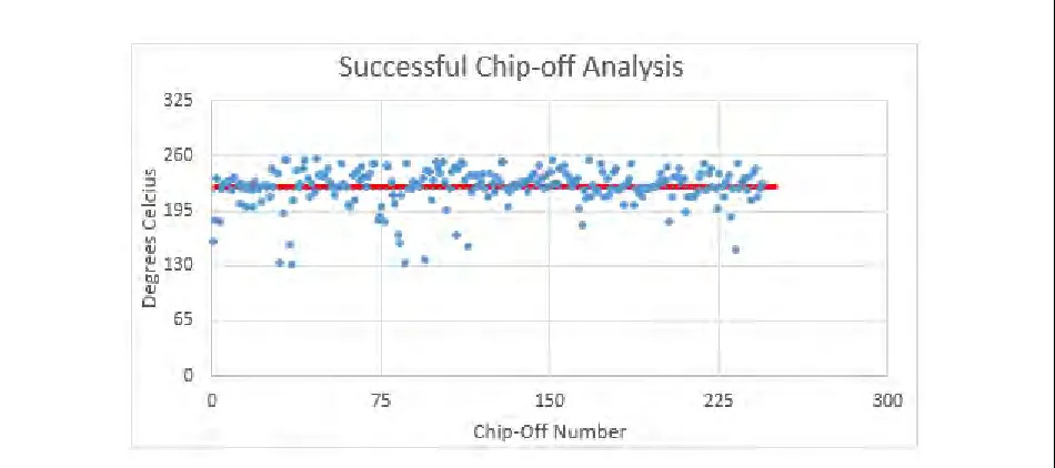
Figure 1. Temperature distribution of chips successfully read.
Unsuccessfu
l
Chip-off Analysis
313
250
"'
•
•
•
..
:i
'Cl
•
•
•
•
aj 188
u
•
,5
"'
~ 125till Q) Cl
63
0
0 4 8 12
Chip-off Number
Figure 2. Temperature distribution of chips unsuccessfully read.
7. 2
Im.pact of temperature225 300
•
between the removal temperatures of memory
chips successfully and unsuccessfully read. The
alternative hypothesis of there is a statistical
difference between the removal temperatures
of the memory chips successfully and
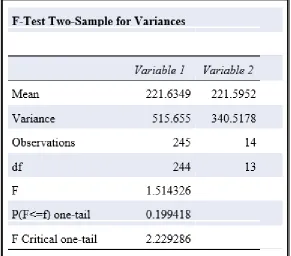
unsuccessfully read. As illustrated in Table 1, F
(1.51) < F critical one tail (2.22) and P (0.199)
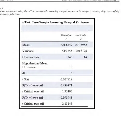
> 0.05. A t-Test: two-sample assuming unequal
variances was also calculated to determine
whether there is a statistical difference between
the means of the memory chips successfully
and unsuccessfully read. For the t-test, the null
and alternative hypotheses remained the same
as in the F-test. Table 2 provides the results of
the t-test with P (0.199) > 0.05 and the t-value
(0.0077) < t-critical value two tail (2.13).
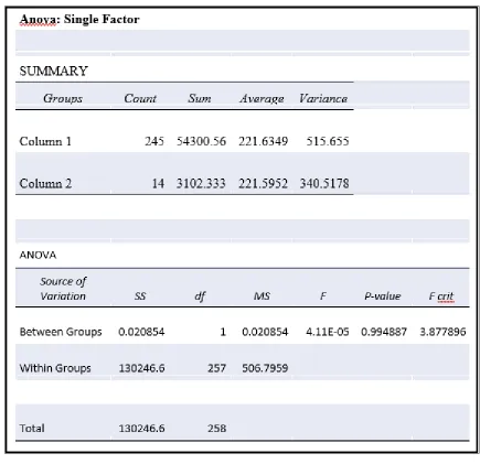
Lastly, an analysis of variance (ANOVA):
single factor was used to again compare the
means between the successful and unsuccessful
read memory chips. The results of the ANOVA
showed the p-value (0.99) > .05 and F
(0.000041) < F crit (3.88) as illustrated in
Table 3. The results from the F-test, t-test and
ANOVA all resulted in the null hypothesis not
being rejected as there was not a statistical
difference between the temperatures of
memory chips successfully and unsuccessfully
read.
Chip-Off Success Rate Analysis Comparing ... JDFSL V13N4
Table 1
Statistical evaluation using the F-test Two Sample for Variance to compare memory chips successfully and unsuccessfully read.
F-Test Two-Sample f:or Variances
Variable J Variable 2
Mearn
221_6349
221_5952
Variance
515_655
340_5178
Observations
245
14
df
244
13F
1-514326
P(F <=f) one-tad.
0_199418
Table 2
Statistical evaluation using the t-Test: two-sample assuming unequal variances to compare memory chips successfully and unsuccessfully read.
t-Test: Two-Samp,]e Assuming Unequal, aria:noes
Variable Variable
1
2Mean 221.6349 221.5952
'\ airiance 515.655 340.5178
Observations 245 14
Hypothesized Mean
Difference 0
df 15
tStat 0.007719
P(T<=t) one-tad. 0.496971
t Critical one-tail 1.75305
P(T <=t) n.-vo-tail 0.993943
Chip-Off Success Rate Analysis Comparing ... JDFSL V13N4
Table 3
An analysis of variance (ANOVA) single factor comparing the means of memory chips successfully and unsuccessfully read.
~ :: Sin~e Factor
SUI\.flvfARY
Groups Count Sum Avera~e Variance
Column 1 245 5430056 221-6349 515.655
Column2 14 3102.333 221.5952 340.5178
AINOVA
Source of
Variation
ss
df MS F P-valueF
ffft
Between Groups 0.020854 1 0.020854 4 ... UE-05 0.994887 3.877896
With in Groups 130246.6 25 7 506. 7959
Total 130246.6 258
7 .3
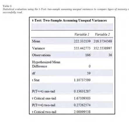
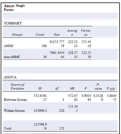
hnpa.ct of
Chiptype
The data obtained from the successful and unsuccessful chip-off procedures were statistically evaluated to determine if a statistical difference exists between the removal temperatures of different types of memory chips successfully read. Due to incomplete data collection, some chip-off analyses were excluded. The F-test two sample for variance was calculated based upon the null hypothesis there is no statistical difference between the removal temperatures of eMMC
single factor was used to compare the means between the eMMC and non-eMMC types of memory chips. The results of the ANOV A showed the p-value (0.34) > .05 and F (0.90)
<
F crit (3.88) as illustrated in Table 6. Like the previous statistical evaluations, the results of the ANOVA could also not reject the null hypothesis.Table 4
Statistical evaluation using the F-test Two Sample for Variance to compare types of memory chips successfully and
unsuccessfully read.
F-Te:st Two-Sample for Varialilces
Variable
1
Variable 2Mean 222332139 218_3 734568
\ ariance 555-442775 352-5538997
Observaitions 186 36
df
185 35F 1-57548328
P(F<=f) one-tai] 0_05587099
Chip-Off Success Rate Analysis Comparing ... JDFSL V13N4
Table 5
Statistical evaluation using the t-Test: two-sample assuming unequal variances to compare types of memory chips successfully read.
t-Test: Two-Samp,le Assuming Unequal Variances
Variable 1 Variable2
Mean 222.332139 218.3734568
Variance 555.442775 352.5538997
Observations 186 36
Hypothesized Mearn
Difference 0
df
59tStat 1.10737599
P(T <=t) one-tai] 0.13631287
t Critical one-tail 1.67109303
P(T<=t) two~tail 0.27262574
Table 6:
An analysis of variance (ANOVA) single factor comparing the means of different types of memory chips successfully read.
A,un
:
Single FactorSUM].AARY
Ave.rag Varian
Groups Count Sum e ce
41353.777 222.33 555.44
elvlMC 186 78 21 28
7861.4444 218.37
35255
non-clvllvfC
A
OVA
Source of Variation
Benveen Groups
\Viithi.n Groups
Total
36
ss
472.6761 17
115096.3
115568.9 76
8.
DISCUSSION OF
RESULTS
df
The statistical evaluation of the data obtained from the chip-off analysis conducted at the Dixie State University Computer Crime Lab helped to confirm many of the assumptions laid out in the hypotheses. This evaluation also
44 35 39
P
-}JS F value F g;jJ_
472.67 0.9034 0.3428 3.8840
1 61 93 9 75
523.16
220
5221
helped to solidify some of the previous research conducted on this topic regarding the use of the thermal chip-off process and the introduction/presence of bit errors in flash memory as presented in the literature review.
Chip-Off Success Rate Analysis Comparing ...
enough sample size to use for comparison
against memory chips successfully read. The mean temperatures for both successfully and
unsuccessfully read memory chips fell within .03 degrees Celsius of each other. During
statistical evaluation, this difference proved to not be statistically different using either a F-test, t-test or ANOVA. Additionally, when
examining the scatter plot from both groups,
the temperatures primarily fell between 150
and 250 degrees Celsius. Those few chip-off analyses that feel below the temperature range
of 150 degrees Celsius were minimal in number
and generally associated with non-eMMC memory chips affixed to the circuit board without the use of epoxy. These lower temperatures were not unexpected since the
lack of epoxy on the memory chips results in reduced temperatures for the memory chip removal.
To determine if these lower temperatures
seen m non-eMMC memory chips were
significantly different than those temperatures seen in eMMC memory chips, the groups were evaluated using the F-test, t-test and ANOVA. Again, the results of the statistical evaluation
found no statistical difference between the two groups. This finding is surprising especially when considering the research from the literature review found an increase in the
introduction rate of bit errors when the
temperatures increased.
9.
S ~ Y
AND
RECOJVIJVIENDATIONS
The use of digital forensics by law enforcement has steadily increased since the introduction of the first mobile device into the marketplace.
Many different software and hardware options
are now available to analyze the majority of digital devices. Occasionally, the presence of passcode/pattern locks or damages to the
digital devices, prevent the use of typical software and hardware options. Thermal
chip-JDFSL V13N4
off analysis has become a viable option for
gaining access to the user data stored on digital devices that would otherwise not be
accessible. The data used in this research was
collected from the Dixie State University
Computer Forensic Lab where thermal chip-off
analysis is conducted for law enforcement
agencies across the county. The literature review used in this research was primarily focused on the possible causes of bit errors in flash memory and viable alternatives to the thermal chip-off process
The results of the statistical evaluation of the data collected from the flash memory
chip's unsuccessful and successful read found the two groups were the same. The same
results occurred when comparing eMMC and
non-eMMC flash memory.
The data used for this research was
collected from a single forensic lab. Future research should elicit data from different forensic lab in order to increase the sample size
of memory chips unsuccessfully read. Additionally, research comparing the thermal and non-thermal based chip-off analysis could help to determine if there a statistical
advantage exist from of one type of process over the other.
In the coming years, the introduction of
encrypted devices from the manufactures could
prove problematic for forensic examiners
relying upon chip-off a