Volume-5 Issue-2
International Journal of Intellectual Advancements
and Research in Engineering Computations
Harmonic reduction in converter by using selective harmonic elimination
technique
1. Ajith.G 2.Dinesh Chandar.G 3.Gobinath.T 4.Manoj Prabahar .M
E-Mail: [email protected]
UG Scholars, Department of EEE,
Nandha Engineering College (Autonomous), Erode.
5. Prabhakaran.S, Professor, Department of EEE, Nandha Engineering College (Autonomous), Erode.
Abstract:- This paper presents a technique to
spot installation harmonics in period of
time mistreatment signals obtained from grid connected
power electronic converters. The projected harmonics
estimation has potential applications in distributed energy
systems; the theoretical and experimental analysis of
the changed SEPIC device is given during this paper.
The projected device operates in DCM. Because
the device operates in DCM it acts as a voltage follower id
est. the input current follows the input voltage. The voltage
across the switch is reduced. Furthermore a
digital management technique is employed to scale back the
third harmonic input current distortion. Finally, 100W
power issue correction circuit was developed
with associate operational potency of ninety eight.
Index Terms- Potential electrical device, Current electrical
device, SEPIC module. liquid crystal display show,
ATMEGA-8, Protius 8, AVR studio.
I.INTRODUCTION
Single section AC-DC converters (rectifiers) square
measure common in power provides that type interface
between utility power offer and equipment connected to
them. Uncontrolled single section diode bridge rectifiers
with output electrical phenomenon filter draw
non-sinusoidal currents . This causes high input current doctor's
degree and low input power issue that is harmful to utility
power offer. Within the past passive filters consisting of
passive filters consisting of Single section AC-DC
converters (rectifiers) square measure common in
power provides that type interface between utility
power offer and equipment connected to them.
Uncontrolled single section diode bridge rectifiers with
output electrical phenomenon filter draw non-sinusoidal
currents. This causes high input current doctor's degree and
low input power issue that is harmful to utility
power offer. Within the past passive filters consisting of
huge L and C at the input was wont to cut back current
distortion (THD) at the
value of more power issue and potency reduction. With the
event of power natural philosophy, active filtering
techniques are wont to alleviate these issues.
These enclosed harmonic current injection and use of
DC-DC device between rectifier and cargo. The
DC-DC device between rectifier and
cargo has several potential configurations together
with those of bridgeless configuration. Recently some
configurations and techniques square measure being
investigated for input current switch by providing switch
between supply and rectifier. to this point Boost, Buck,
Buck-Boost and Ćuk configurations are investigated for
single section rectifier input current switch.
The rectifier with output filter electrical condenser is
termed a standard AC-DC utility interface. The
filter electrical condenser reduces the ripples gift within
the output voltage. though a filter electrical
condenser considerably suppresses the ripple from the
output voltage, it introduces distortions within the input
current and attracts current from the
provision discontinuously briefly pulses. This
introduces issues together with reduction of
accessible power and raised loss.
To study standard switch mode single section
AC-DC device topologies at the input facet of the
rectifier together with SEPIC, Inverse SEPIC
and letter topologies for AC-DC conversion with high input
PF, low input current THD and high potency, to
enhance the full harmonic distortion (THD) of
single section rectifiers mistreatment switch mode
topologies of Buck, Boost, Buck-Boost, Ćuk, SEPIC,
Inverse SEPIC and alphabetic character converters at the
input aspect of the rectifiers, Input current of controlled
single section rectifiers are nearly curving and can be
in section with input voltage. Absolute face bridge
configuration are replaced so advantages can are available
in handy like low physical
phenomenon and shift losses so on. High
performances are achieved i.e. high PF and potency
similarly as low doctor's degree.
II. EXISTING SYSTEM
In existing system, harmonics reduction is
finished by victimization harmonics compensation
techniques implementing PI
controller. it's not adaptative management, thus error answer
won't be correct. there's no management technique for
reactive power management.
BLOCK DIAGRAM
FIG 2.1 EXISTING BLOCK DIAGRAM
PROBLEMS OF CONVENTIONAL INTERFACE:
The large harmonic content and also the ensuing poor
power issue (PF) of operation of the traditional
rectifier--capacitor kind interface causes many issues to the
utility provide. a number of them area unit listed
below because of harmonic elements - as a result of the
non-zero supply electrical resistance within the utility provide,
the harmonic currents flowing through the traditional
AC-DC utility interface can cause a distortion within
the voltage wave shape at the purpose of common
coupling. this could cause malfunction
of facility protection, masses and metering devices. Besides
voltage wave shape distortion, harmonic elements can
also cause the issues of heating of neutral line, distribution
transformers and distribution lines, interference with
communication and management signals, over
voltages because of resonance conditions.
(2)Due to poor PF - Poor power issue of operation implies
ineffective use of the var ratings of the
utility instrumentation like transformers, distribution lines
and generators. Also, it places a restriction on the
whole instrumentation load which will be connected to a
typical home or workplace wall-plug
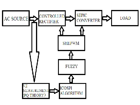
III.PROPOSEDSYSTEM
In projected system, Selective Harmonic Elimination Pulse
with Modulation is enforced therefore harmonics created is
low. As a result of MLI harmonics compensation,
harmonics are but a pair of in projected system and still as
reactive power. Implementation of fuzzy
controller can scale back the latency for harmonics and
reactive power compensation but 2µs.
BLOCK DIAGRAM
FIG 3.2 PROPOSED BLOCK DIAGRAM
In projected system, voltage and current feedback is 1st fed
to reactive power and
harmonics expert and once estimating it's given to fuzzy
controller. Here, SHEPWM technique
and structure electrical converter is employed for harmonics
reduction and reactive power compensation.
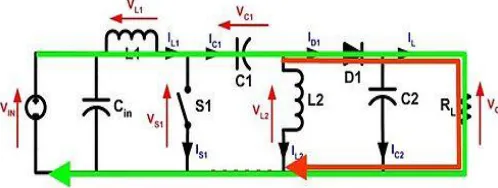
SINGLE-ENDED PRIMARY INDUCTOR CONVERTER:
Fig3.3 Schematic of SEPIC.
The single-ended
primary-inductor device (SEPIC) may be a variety
of DC/DC device permitting the electrical potential
(voltage) at its output to be bigger than, less than, or up
to that at its input. The output of the SEPIC is management
led by the duty cycle of the control electronic transistor. A
SEPIC is basically a lift device followed by a
buck-boost device, thus it's almost like a conventional
buck-boost device, however has blessings of getting non-inverted
output (the output has a similar voltage polarity because
the input), employing a series electrical device to couple
energy from the input to the output
(and therefore will respond additional graciously to a
short-circuit output), and being capable of true
shutdown: once the switch is turned off, its output drops
to zero V, following a reasonably hefty transient dump of
charge.
SEPICs square measure helpful in
applications within which electric battery voltage are
often on top of and below that of the
regulator's supposed output. for instance, one atomic
number 3 particle battery generally discharges from four.2
volts three |to three} volts; if alternative elements need 3.3
volts, then the SEPIC would be effective. SEPICs are useful
in applications in which a battery voltage can be above and
below that of the regulator's intended output. For example, a
single lithium ion battery typically discharges from 4.2 volts
to 3 volts; if other components require 3.3 volts, then the
SEPIC would be effective.
The schematic diagram for a basic SEPIC is shown in
Figure one. Like alternative switched mode
power provides (specifically DC-to-DC converters), the
SEPIC exchanges energy between the capacitors and
inductors so as to convert from one voltage to a
different. The number of energy changed is controlled by
switch S1, that is often a electronic transistor like a
MOSFET. MOSFETs provide a lot of higher
input resistivity and lower free fall than bipolar junction
transistors (BJTs), and don't need biasing resistors as
MOSFET change is controlled by variations in
voltage instead of a current, like BJTs).
CONTINUOUS MODE
A SEPIC is alleged to be in continuous-conduction mode
("continuous mode") if the present through the electrical
device L1 ne'er falls to zero. Throughout a SEPIC's
steady-state operation, the common voltage across electrical
device C1 (VC1) is adequate to the input voltage (Vin). as a
result of electrical device C1 blocks electricity (DC), the
common current through it (IC1) is zero, creating electrical
device L2 the sole supply of DC load current. Therefore, the
common current through electrical device L2 (IL2) is that
the same because the average load current
and thence freelance of the input voltage.
Looking at average voltages, the subsequent are
often written: Because the common voltage of VC1
is adequate to VIN, VL1 = −VL2. For this reason, the
2 inductors are often wound on constant core. Since the
voltages square measure constant in magnitude, their effects
of the coefficient are going to be zero, presumptuous the
polarity of the windings is correct. Also, since the
voltages square measure constant in magnitude, the ripple
currents from the 2 inductors are going to be equal in
magnitude.
The average currents are often summed as follows
(average electrical device currents should be zero):
once switch S1 is turned on, current IL1 will increase and
therefore the current IL2 goes a lot of negative.
(Mathematically, it decreases attributable to arrow
direction.) The energy to extend the present IL1 comes from
the input supply. Since S1 could be a moment closed, and
therefore the instant voltage VC1 is closed.
Figure 3.4: With S1 closed current increases through L1
(green) and C1 discharges increasing current in L2 (red)
When switch S1 is turned off, this IC1
becomes identical because the current IL1, since
inductors don't enable instant changes in
current. This IL2 can continue within the negative
direction, actually it ne'er reverses direction. It may be seen
from the diagram that a negative
IL2 can increase this IL1 to extend this delivered to the
load. Victimization Kirchhoff's Current Law, it may
be shown that ID1 = IC1 - IL2. It will then be terminated,
that whereas S1 is off, power is delivered to the load
from each L2 and L1. C1, but is being charged by
L1 throughout this off cycle, and can successively recharge
Figure: 3.5 With S1 open current through L1 (green) and
current through L2 (red) produce current through the load
Because the potential (voltage) across electrical
condenser C1 could reverse direction each cycle, a
non-polarized electrical condenser ought to be used. However, a
polarized Ta or electrical condenser is also utilized in some
cases,[2] as a result of the potential (voltage)
across electrical condenser C1 won't amendment unless the
switch is closed long enough for a 0.5 cycle of resonance
with electrical device L2, and by now this in electrical
device L1 may well be quite giant.
The electrical condenser CIN is needed to scale back the
results of the parasitic inductance and internal resistance
of the ability offer. The boost/buck capabilities of the
SEPIC ar doable as a result of electrical condenser C1
and electrical device L2. Electrical device L1 and switch
S1 produce a customary boost device that generates a
voltage (VS1) that's over VIN, whose magnitude is set by
the duty cycle of the switch S1. Since the common voltage
across C1 is VIN, the output voltage (VO) is VS1 - VIN. If
VS1 is a smaller amount than double VIN, then the output
voltage are but the input voltage. If VS1 is bigger than
double VIN, then the output voltage arebigger than the input
voltage.
The evolution of switched-power provides may be seen by
coupling the 2 inductors in a
very SEPIC device along, that begins to match a Fly
back device, the foremost basic of the transformer-isolated
SMPS topologies.
DISCONTINUOUS MODE:
A SEPIC is alleged to be in discontinuous-conduction mode or discontinuous mode if this through the inductance L1 is allowed to fall to zero.
FIG 3.6 PROPOSED CIRCUIT DIAGRAM
A SEPIC may be a form of DC-DC device permitting the
electrical potential (voltage) at its output to be but, larger
than, or capable that at its input; the output of the SEPIC is
management led by the duty cycle of the control
semiconductor. SEPIC is effectively a lift device followed
by a buck-boost device, consequently it's wish to a
traditional buck-boost device, apart from has blessings of
getting non-inverted output (the output has a similar voltage
polarity because the input), passing through a series
electrical condenser to couple energy from the input to the
output (and so will respond additional graciously to a
short-circuit output), and having the ability of factual shutdown:
when the switch S1 is turned off, its output drops to zero V,
following a rather hefty transient abandon of charge.
SEPICs area unit useful in applications within which A
battery voltage may be higher than and below that of the
regulator's meant output The schematic diagram for a basic
SEPIC is shown in Figure three like different switched
mode power provides (specifically DC-to-DC converters),
the SEPIC interactions energy between the capacitors and
inductors so as to convert from one voltage to a different.
The number of energy changed is in switch S1, that is
classically a semiconductor like a MOSFET. MOSFET
offers abundant higher input electric resistance and lower
free fall than bipolar junction transistors (BJTs), and don't
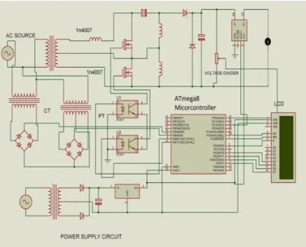
microcontroller. Liquid crystal {display|LCD|digital display
|alphanumeric display} is employed to display harmonics
level. Here optocoupler U1, U2 is employed for MOSFET
driver circuit.
IV.RESULTSANDDISCUSSION
The experiments were conducted to judge the performance of the planned methodology. The results bestowed during this paper mark the start of our efforts to create a Harmonic Reduction. Power issue correction has embrace for input power potency Icospi rule has influencing during this system for compensate the Harmonics its terribly correct and quick response therefore harmonics is lower than two SHEPWM is employed to cut back harmonic losses in MLI.
V.CONCLUSION
The harmonic minimization shapes the input current of off-line power provides to maximize the power offered from the mains. Ideally, the electrical appliance ought to gift a load that features a pure electrical device, so the reactive power drawn by the device is zero. The input current harmonics square measure absent, the input current could be a good duplicate of input voltage (sine wave). This drawn from the mains is at a minimum for the power needed to perform the required work, and this minimizes losses and value associated. The liberty from harmonics additionally minimizes interference with alternative devices being high-powered from constant supply.
REFERENCES
[1] B. Singh, B. N. Singh, A. Chandra, and K. Al-Haddad,
A. Pandey, D. P. Kothari, “A review of single-phase
improved power quality AC-DC converters”, IEEE
Transactions on Industrial Electronics, Vol. 50, No. 5, Oct.
2003, pp 962 – 981.
[2] O. Garcia, J. A. Cobos, R. Prieto, P. Alou, and J.
Uceda, “Single Phase Power Factor Correction: A Survey”,
IEEE Transactions on Power Electronics, Vol. 18, No. 3,
May 2003, pp. 749-755.
[3] H. Wei and I. Batarseh, "Comparison of Basic
Converter Topologies for Power Factor Correction," in
Proceeding Southeastcon'98, 1998, pp. 348-353.
[4] J. Salmon, “Techniques for minimizing the input
current distortion of current-controlled single-phase boost
rectifiers”, IEEE Tran. on Power Electronics, 1993, pp.
509–520.
[5] R. Erickson and M. Madigan, “Design of a simple
high- power-factor rectifier based on the flyback converter”,
IEEE applied power electronics conference (APEC), 1990,
pp. 792–801.
[6] D. Tollik and A. Pietkiewicz, “Comparative Analysis
of 1-Phase Active Power Factor Correction Topologies,” in
Proc. Int. Telecommunication Energy Conference,
Washington DC, USA, Oct. 1992, pp. 517-523.
[7] O. L´opez, L. Vicu˜na, M. Castilla, J. Matas, and M.
L´opez, “Sliding- Mode-Control Design of a High-Power-Factor Buck–Boost Rectifier” IEEE Transactions on
Industrial Electronics, Vol. 46, No. 3, Jun 1999, pp. 604 –
612.
[8] M. S. Patil, and S. P. Patil, "Single-Phase Buck-Type
Power Factor Corrector with Lower Harmonic Contents in
Compliance with IEC 61000-3-2" International Journal
ofEngineering Science and Technology, Vol.
2(11), 2010, pp. 6122- 6130
[9] M. Brkovic and S. Cuk, “Input current shaper using
Cuk converter”, 14th International Telecommunications
Energy Conference, INTELEC'92, Oct. 1992, pp.532- 539.
[10] P. F. Melo, R. Gules, E. F. R. Romaneli, and R. C.
Annunziato, “A Modified SEPIC Converter for
High-Power-Factor Rectifier and Universal Input Voltage
Applications”, IEEE Transactions on Power Electronics,
Vol. 25, No. 2, Feb 2010, pp. 310-321.
[11] D. Maksimovic, J. Yungtaek, and R. Erickson,
“Nonlinear-Carrier Control for High Power Factor Boost Rectifiers”, Applied Power Electronics Conference and
Exposition, Dallas, Texas, USA, Vol. 2, March 1995, pp.
635-641.
[12] T. Tanitteerapan and E.Thanpo, “Negative Slope
Converters in CCM Operation”, World Academy of Science,
Engineering and Technology, 2009, pp. 1084-1089.
[13] M. Kazerani, P. D. Ziogas and G. Joos, “A Novel
Active Current Wave Shaping Technique for Solid-State
Input Power Factor Conditioners”, IEEE Trans. on
Industrial Electronics, Vol. 38, No.1, Feb. 1991, pp.72-78.
[14] L. Huber, Y. Jang, and M. Jovanovic, “Performance
Evaluation of Bridgeless PFC Boost Rectifiers,” IEEE
Trans. on Power Electronics, Vol. 23, No. 3, May 2008, pp.