Sharma et al. World Journal of Engineering Research and Technology
A LOW POWER HIGH SPEED 32/33 PRESCALER BASED ON DIVIDE
BY 2/3 WITH TRUE SINGLE PHASE CLOCK LOGIC
Neetu Sharma*1 and Uma Nirmal2
1
M.tech. VLSI, CET, Mody University of science & technology, Laxmangarh, Sikar,
Rajasthan, India.
2
Assistant Professor, CET, Mody University of science and technology, Laxmangarh, Sikar,
Rajasthan, India.
Article Received on 03/04/2018 Article Revised on 24/04/2018 Article Accepted on 14/05/2018
ABSTRACT
A low-power high-speed based on divide-by-2/3 divider, dual modulus
divide by32/33 prescaler is designed with characteristics of low supply
voltage, high operating frequency and low-power consumption. The
design uses TSPC logic to decrease the power consumption and
increase the noise performance. The circuit is simulated at 180 nm low
power CMOS process. The simulated results show that the highest operating frequency is up
to 28.57 GHz and running at a power supply of 1v, the circuit consumes only 1.01 µW at
input frequency.
KEYWORDS: TSPC, Prescaler, low voltage, low power, dual modulus prescaler, frequency divider, Frequency Synthesizer
I. INTRODUCTION
The power utilization of RF building squares is a bottleneck for long battery lifetime. The
frequency divider, working at the most noteworthy frequency, is a basic segment for low
power design. The expanding interest of cell phones requires low-power circuit outlines for
longer battery life, so the fast prescaler with low power utilization turned out to be critical.[1]
A few topologies are accessible for prescaler in the GHz range, including MOS current-mode
logic (CML), TSPC logic and extended TSPC logic. The CML circuit disperses high power
wjert, 2018, Vol. 4, Issue 3, 346-354.
World Journal of Engineering Research and Technology
WJERT
www.wjert.org
ISSN 2454-695X Original Article
SJIF Impact Factor: 5.218
*Corresponding Author
Neetu Sharma
M.tech. VLSI, CET, Mody
University of science &
technology, Laxmangarh,
Sharma et al. World Journal of Engineering Research and Technology
and is utilized for high frequency where different topologies can't work. It has been normally
trusted that there is a speed-power exchange off between the two fundamental topologies: the
E-TSPC based topology is appropriate for high speed applications however experiences high
power utilization, while the TSPC based prescaler is better for low power applications with
constrained speed. Contrasted with the traditional CML circuit, the TSPC circuit is more
favorable for low voltage task since all FETs in the TSPC circuit work in the exchanging
mode though all stacked FETs in the CML circuit must be biased in the saturation region.[1]
Dual modulus prescaler is a basic building block in the fraction N frequency synthesizer in
light of PLL. SCL structure is utilized to reduce the switching noise, and enhance the
operating speed of prescaler. The most test in the design of high speed prescaler is to enhance
the operating speed of D-type flip-flops.[2]
To date, the majority of the fast dual modulus prescalers utilize SCL, bringing about high
power utilization. Then again, utilizing dynamic logic methods, in particular, E-TSPC
prompts low power utilization, compact design and broadband task. Notwithstanding, the
E-TSPC logic has been just utilized as a part of plan of low speed prescaler.[3]
Contrasting and regularly utilized SCL, dynamic logic reduces the capacitive load along these
lines decreases the power utilization. The dynamic logic circuits have shorter
interconnections between the transistors, consequently littler interconnection capacitances. In
this manner, the W/L ratio of the transistors can be been littler, consequently decreasing the
power utilization.[3]
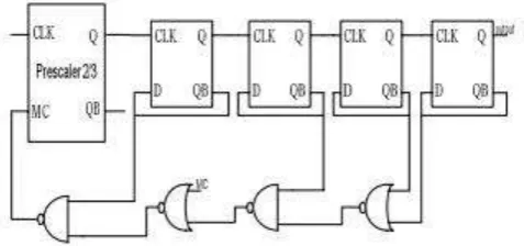
II Dual modulus divide-by-32/33 prescaler design
The primary parameters to be considered in designing high speed digital circuits are the
operating frequency and power consumption.[4] The operating frequency is restricted by
propagation delay of the circuit. The power utilization of CMOS digital circuit is given by:
Where fclk is the clock frequency, α signifies node transition activity factor, Vdd is the supply
voltage and CL is the load capacitance. The power utilization is just contributed by switching
activities in the CMOS advanced circuits. The completely programmable divider is proficient
Sharma et al. World Journal of Engineering Research and Technology
The primary phase of Dual modulus divide by 32/33 the prescaler which works most
noteworthy frequency, devours much power because of switching between 32 and 33 division
ratios. The prescaler consists of a synchronous 2/3 divider followed by an asynchronous
divide by 16, unit as shown in Fig. 1. The flip-flop in this prescaler is the dynamic logic
TSPC D flip-flop. The TSPC dynamic logic 2/3 asynchronous stage is utilized instead of
E-TSPC as the later one has high switching power and short circuit power where as previous
has diminished capacitive loads.
The sizes of transistors in the TSPC flip-flops and digital gates in divide by 2/3 is
appropriately scaled to accomplish fast and low power utilization.
Fig. 1: Conventional divide by 32/33 dual modulus prescaler A. Divide-by-2/3 prescaler.
The ETSPC based ÷2/3 unit Design-I in[6] is depicted in Figure 2. At the point when the
modulus control signal MC is consistently high, the output of D Flip-Flop1 will be stopped to
accomplish the ÷2 work. At the point when MC is set to low, it plays out the ÷3 work. In any
case, both DFFs work regardless of whether DFF1 Doesn't take an interest in the ÷2 work.
The limitation of design-I circuit is that the power dissipation due to short circuit path is more
since the load capacitance is large, the operating frequency is limited and the critical path is
long.
Figure 3 shows the ETSPC based ÷2/3 unit Design-II[7] The output of DFF1 will be clogged
to accomplish the ÷2 work, when the modulus control signal MC is consistently high. At the
point when MC is coherently low, it works as the ÷3. When MC=0 in ÷2 mode, short circuit
path is absent in the second and third phase of D Flip-Flop1 and thus the power consumption
is decreased. Design-II is superior to design-I since short circuit path is absent and
Sharma et al. World Journal of Engineering Research and Technology
In ÷ 2/3 prescaler Design-II transistor count is less thus power dissipation and delay is less as
compare to design-I.
Fig. 2: ETSPC based ÷ 2/3 Prescaler Design-I.
Fig. 3: ETSPC based ÷ 2/3 Prescaler Design-II.
Figure 4,5 shows the output waveform of ÷2 counter design-II and ÷3 counter Design-II
respectively. Design-II operating at 1.2V has the transistor count of 16 and is Working at
Sharma et al. World Journal of Engineering Research and Technology
Fig. 5: Output waveform of Divide-By-3 Counter design-II.
Table I illustrates simulation performances of dual modulus 2/3 prescalers and it is clearly
visible that the results of Design-II is much better than Design-I. The Design-II can operate
properly up to 1.2V. Moreover, the transistor count in implementing the circuit as well as the
power dissipation of Design-II[7] is much lower than the previous prescaler implemented in
Design-I.[6]
Table I: Performance analysis of different dual modulus 2/3 prescalers. Design Parameters Design-I[6] Design-II[7]
Transistor Count 18 16
Process( m) 0.18 0.18
Voltage(V) 1.2 1.2
Power(mW) ÷ 2 mode 1.05 1.02
Power(mW) ÷ 3 mode 1.13 1.11
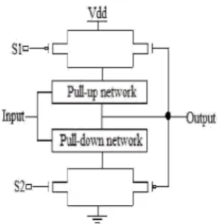
B. Sleepy keeper approach
In this philosophy combination of PMOS and NMOS transistor[8] is coupled parallel between
pull up network and Vdd and also pull down network and GND[9] as appeared in Fig.7. The
NMOS transistor of draw up rest transistor is joined to PMOS pull down rest transistor. As
NMOS rest transistor which rail off the course from Vdd to GND is associated with GND and
PMOS transistor which is associated with Vdd, NMOS transistor isn't turn ON that is the
reason it won't competently pass Vdd. This trouble can be overwhelmed by maintaining yield
esteem "1" in rest mode by joining NMOS to Vdd. PMOS transistor which is connected to the
Sharma et al. World Journal of Engineering Research and Technology
yield esteem equivalent to "0" in rest mode. This strategy decreases the power well and keeps
up the fitting rationale of the circuit with lessened zone.[10]
Fig. 6: Sleepy keeper approach.
III Simulation & Results of propose ÷ 32/33 DMP designs A. Proposed Divide-by-32/33 Dual Modulus Type -I Prescaler
The Schematic of divide by 32/33 dual modulus Type-I prescaler using E-TSPC based
divide-by-2/3 Prescaler Design I has been designed and moreover the NAND and NOR gate
has been designed through sleepy keeper approach for further power reduction.
B. Proposed Divide-by-32/33 Dual Modulus Type -II Prescaler
The Schematic of divide by 32/33 dual modulus Type-II prescaler using E-TSPC based
divide-by-2/3 Prescaler Design II has been shown in figure 7 and moreover the NAND and
NOR gate has been designed through sleepy keeper approach for further power reduction.
Sharma et al. World Journal of Engineering Research and Technology
The simulation waveform of design as divide by 32 counter (when MC=0) is shown in figure
8 and similarly as divide by 33 counter (when MC=1) is shown in figure 9.
Fig. 8: Simulation waveform of divide by 32 counter.
Fig. 9: Simulation waveform of divide by 33 counter.
Table II illustrates simulation performances of dual modulus 32/33 prescalers and it is clearly
Sharma et al. World Journal of Engineering Research and Technology
1.0v which is lower than the supply voltage of Type-I. The power dissipation of Type-II is
much lower than the Type-I prescaler. Table III illustrates simulation and comparison results
of different dual modulus 32/33 prescalers are presented. The proposed design reduces most
of circuit current power and consumes less power than all the conventional designs. The
proposed designs can still work at a high speed and high operating frequency.
Table II: Performance of different dual modulus 32/33 prescalers using 2/3 prescaler. Design Parameters Type-I Type-II
Process 0.18 0.18 Voltage(V) 1.8 1 Average Power(uW) 1.3 1.01
Table III: Performance summary and its comparison with low power dual modulus 32/33 prescaler.
Parameter 2004[2] 2005[3] 2007[4] 2009[5] 2015[1] This work
Technology Used (µm) 0.25 0.18 0.18 0.09 0.18 0.18 Supply Voltage(V) 2.5 1.8 1.8 1.2 1.2 1 Operating Frequency(GHz) 3.2 5.3 2.55 6 17.9 28.57 Power Dissipation 4.6 2.53 1.7 1.19 0.245 1.01
IV. CONCLUSION AND FUTURE SCOPE
In this paper, I have implemented divide by 32/33dual modulus prescaler using 2/3 prescaler
with better power and speed performance. The simulation and comparison results are
presented. It confirms that the proposed design reduces most of circuit current power and
consumes less power than all the conventional designs. Besides, the proposed designs can
still work at a high speed to meet the demand of high speed to meet the demand of high
operating frequency.
REFERENCE
1. Song Jia, Shilin Yan, Yuan Wang and Ganggang Zhang, “A Low-Power High-Speed
32/33 Prescaler Based on Novel Divide-by-4/5 Unit with Improved True Single-Phase Clock Logic”, Key Laboratory of Microelectronic Devices and Circuits, Institute of
Microelectronics, Peking University, Beijing 100871, CHINA , 2015 IEEE.
2. Wen-Rong Yang, Jia-Lin Cao, Fen Ran, and .linn Wnng, “A 2.5 GHz CMOS
Dual-modulus Prescaler for RF Frequency Synthesizer”, Microelectronic Research
Sharma et al. World Journal of Engineering Research and Technology
3. Golsa Ghiaasi and Mohammed Ismail, “A CMOS Broadband Divide-by-32/33 Dual
Modulus Prescaler for High Speed Wireless Applications”, 0-7803-9197-7/05/$20.00 ©
2005 IEEE.
4. M. Vamshi Krishna, J. Xie, W. M. Lim, M. A. Do, Senior MIEEE, K. S. Yeo and C. C. Boon, “A Low Power Fully Programmable 1MHz Resolution 2.4GHz CMOS PLL Frequency Synthesizer”, 1-4244-1525-X/07/$25.00 © 2007 IEEE.
5. Xu Tailong and Meng Jian, “Design of A 1.2-v 6-GHz 1.19-mW Divide-by-32/33 Prescaler”, National Natural Science Foundation of China, 978-1-4244-4994-1/09/$25.00
©2009 IEEE.
6. S. Pellerano, and S.Levantino, “A 13.5 mW 5 GHz Frequency Synthesizer with Dynamic
Logic Frequency Divider”, IEEE Journal of Solid-State Circuit, February 2004; 39(2).
7. X.P. Yu, M.A. Do, W.M. Lim, K.S. Yeo, J.-G. Ma,: “Design and Optimization of the
Extended True Single-Phase Clock-Based Prescaler” IEEE Transactions on Microwave
Theory and Techniques, Nov. 2006; 54(11).
8. Raina Jain, Mrs. Uma Nirmal and Monika Gautam, “Low Voltage Low Power 4/5 Dual Modulus Prescaler in 180nm Technology”, International Conference on Research
Advances in Integrated Navigation Systems (RAINS - 2016), May 06-07, 2016; R. L.
Jalappa Institute of Technology, Doddaballapur, Bangalore, India.
9. P. K. Pal, R. S. Rathore, A. K. Rana and G. Saini³New low-power techniques: Leakage
Feedback with Stack & Sleep Stack with Keeper´ International Conference on Computer
and Communication Technology (ICCCT), Allahabad, Uttar Pradesh, 2010; 296-301.
10.S.H. Kim and V.J Mooney, “Sleepy Keeper: a New Approach to Low-leakage Power
VLSI Design,” IFIP International Conference on Very Large Scale Integration, Nice,
China, 2006; 367-372.
11.Neetu Sharma and Mrs. Uma Nirmal, “Review of High Speed and Low Power ETSPC Based ÷ 2/3 Prescaler”, International Journal of Allied Practice, Research and Review,