Design & Development of an Embedded Camera
with Built in Image Processing
Ajay Kumar Naik G. C. Naga Anusha
Assistant Professor Assistant Professor
Department of Electronics & Communication Engineering Department of Electronics & Communication Engineering
CBIT, Proddatur, India CBIT, Proddatur, India
Abstract
This paper involves the design and development of an embedded camera with built in image processing. For this, initially the components have been chosen based on low cost without compromising on fit, form and function. The design (schematics and layout) was implemented using Or CAD tool. This paper also shows some image processing algorithm which can be used for number plate reading simulated using MATLAB. The required code for this algorithm has been developed.
Keywords: OrCAD, MATLAB, Mathematical Morphology
_______________________________________________________________________________________________________
I. INTRODUCTION
The aims is to design and develop an embedded camera with built in image processing. In this scenario, number plate reading is taken as example. The design part consists of several steps such as requirement analysis, design specifications, Schematic Capture in OrCAD, component engineering, PCB Layout design, assembly level Programming and testing. The design specification provides the complete information about the system requirements. The OrCAD tool is used for capturing the schematic, PCB layout and routing. After completion of the PCB layout and routing, gerber files are generated from the tool for PCB fabrication. The required components for assembling on PCB were chosen based on the specifications of the design. The simulation of number plate reading is done in MATLAB using image processing toolbox. The number plate reading is implemented using morphological image processing algorithm. The I2C protocol was implemented using VHDL for programming the image sensor on FPGA.
Objective & Specifications
The objective is to design and develop an embedded camera with built-in image processing and the specifications to design are defined as follows:
Image quality: Monochrome, 1.3MP. Supply voltage: 3.0V to 3.6V. USB connectivity: Yes. Flash LED: Yes. Internal storage: Yes. Signal to noise ratio: 45 dB. Maxi data rate: 48 MPS/48 MHz. Operating temperature: 0oC to +70oC. Object detection: Yes.
As for the above specifications, the major components that are required for designing a camera are image sensor, FPGA, USB controller, voltage regulator (LDOs) and 4GB NAND Flash memory. The table 1 shows the part number of chosen components.
Table – 1
Components & Their Part Numbers Components Part numbers Image sensor MT9M001C12STM
FPGA XC3S200A-4VQG100C USB controller CY7C68013A-100AXC NAND FLASH NAND04GW3B2DN6E
Design Cycle
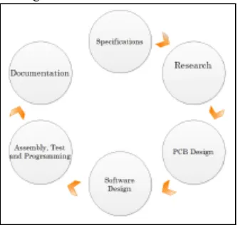
The electronic product design cycle is shown in figure1.
Fig. 1: Product Design Cycle
Specification
Design team gets the specifications from the customer which include specific requirements with a set of constraints on cost, time etc. The customer expects the tentative cost and deadline. The specification can also come from marketing team, if the design is done inside the same company. In this case the marketing team analyses the market situation, consumer requirements and competitor product features to decide on the specification, cost and time to market.
Research
In this step, in-depth study is done on necessary components required to implement the specifications within the targeted costs. Finally, design team comes up with a Block Diagram and tentative list of components required for the design. Timing schedule will be prepared and work is divided among the team.
PCB Design
It includes Schematic Capture, Bill of materials (BOM) and Layout design. There are many tools available for Schematic capture and Layout design. OrCAD 10.0 is used. PCB design starts with Schematic Capture using OrCAD capture CSI, where the connections are made between the ICs and discrete components according to the required functionality disregarding the physical dimensions.
Software Design
Work on software runs in parallel with the PCB Design. This step includes implementation of algorithms. Each product may contain Micro Controller or FPGA as Host Controller. It controls the operation of the product, responds to user inputs to have control over the product.
MATLAB simulation of number plate reading, VHDL simulation of I2C communication between image sensor and FPGA and data storing into a memory have been implemented.
Assembly, Test & Programming
Once the PCB got fabricated, components have to be assembled and the entire board has to be tested. Before programming, simple tests are performed like checking the voltages at all the test points etc. Once the programming is done, all the reliability tests are performed to quantify the accuracy of the output.
Documentation
If the prototype is working successfully, then the product will be moved to production phase. If there are any problems or an y additions and/or deletions suggested by the customer, then next revision will be started with the corrections.
III. EMBEDDED CAMERA DESIGN
Schematic Design
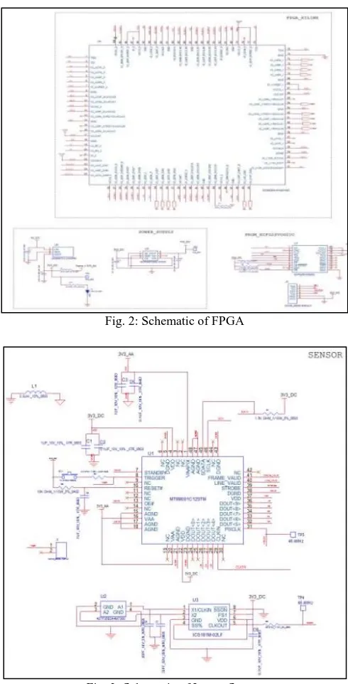
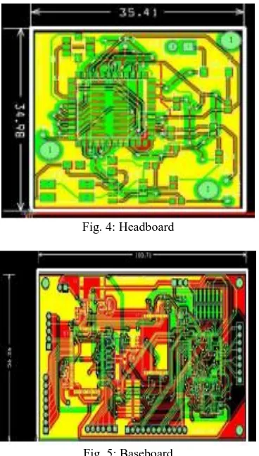
The OrCAD Capture CIS is used for schematic design. This tool used for electronic design automation and also useful for creating electronic schematics and electronic prints for manufacturing printed circuit boards, by using this tool corresponding net list can be generated.
Fig. 2: Schematic of FPGA
Fig. 3: Schematic of Image Sensor
Layout
Fig. 4: Headboard
Fig. 5: Baseboard
The layout routing for this design is done in two different boards Head board and Base board to save the area. Head board consists of mainly image sensor, base board consists of FPGA Processor, NAND Flash and USB Controller. Figure 4 and 5 show the Layouts of the Headboard (includes image sensor) and Baseboard (includes FPGA, flash memory, PROM and power supply section) respectively.
IV. CAMERA TECHNOLOGY
When light falls on the image sensor through the lens, it converts the received amount of light into electrons. The stronger the light intensity, more electrons are generated. These generated electrons are converted into an analog voltage which is then converted into digital by means of A/D converter. CCD (Charge-Coupled Device) and CMOS (Complementary Metal-oxide Semiconductor) sensors are the two different technologies mostly used for capturing.
CCD (Charge-Coupled Device)
The CCD image sensors consist of control circuitry and array of capacitors. A light is projected through lens on to the sensor. This light causes each capacitor to accumulate electric charges corresponding to the light intensity. A control circuit causes each capacitor to transfer its content to its neighbor. The last capacitor in the array sends its charges to an amplifier, which converts the electric charges into voltage and finally these voltages are digitized using A/D converter and stored into a memory.
As compared with CMOS technology, CCD requires more power to convert all the pixels to a data. CCD sensors are more sensitive to light and hence capture high quality images with low noise. CCD sensors also require a higher data rate, since everything has to go through just one output amplifier, or a few output amplifiers.
CMOS (Complementary Metal-Oxide Semiconductor)
V. HARDWARE DESIGN
Block Diagram
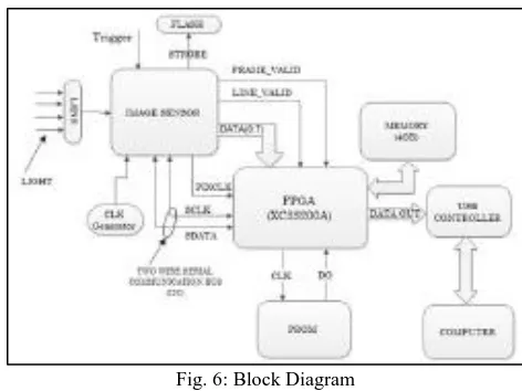
Detailed block diagram of camera is shown in figure 6 and the major components are as follows. 1) Image sensor
2) FPGA 3) Flash memory 4) USB controller.
Fig. 6: Block Diagram
As shown in figure 6, light is projected or focused through lens onto the image sensor which converts the light into an electronic signal.
Image sensor plays an important role in the output image. FRAME VALID (FV) and LINE VALID (LV) are the output signals of the image sensor along with the PIXCLK that is synchronous with valid data. The complete frame of an image is valid when FV is high and each row or line in the frame is valid when LV or ROW VALID (RV) is high. The output data from the image sensor is given as input to the FPGA processor along with FV, LV and PIXCLK. The sensor can be operated in its default mode or can be programmed by the user for Gain, frame rate, frame size, and other parameters. This programming of sensor can be done by accessing all the registers of the sensor by two wire serial communication bus (I2C) interface with 16-bit address and 16-bit data. To capture images, the sensor must first be put into snapshot mode. In snapshot mode, the sensor waits for a TRIGGER signal. When trigger signal is received, sensor sends a strobe signal to flash and one frame of the image is read out. As shown in the figure 6, FPGA is the central processing unit. FPGAs are SRAM based ICs, so once power is off, configured data will be lost. In order to avoid that, an external PROM is used to configure the FPGA as shown in figure 6. FPGA will have some mode select pins to select mode (master/slave). If FPGA is in master mode then it generates the configuration clock (CCLK) that drives the PROM. In response, PROM sends configuration data to FPGA to configure it. FPGA is used to control or program the image sensor for its gain, frame size, and other parameters using SDA and SCLK lines of I2C bus by accessing all the registers of sensor. As shown in figure 6, Memory (4GB) is used to store the image which was sent by the FPGA. Memory will have some address, data and some control lines. FPGA sends address and data through address and data lines of the memory respectively and data will be stored in to the memory location of the address received from FPGA. It also sends data to host computer to which it is connected through USB controller and USB controller converts parallel data to serial data. Now some image processing will be performed on this data, to extract information from it using MATLAB simulation.
VI. ALGORITHM
Mathematical Morphology (MM)
Mathematical morphology is a technique for extracting image information useful in the representation and description of region shape, such as boundaries, skeletons and convex hulls. The basic operations in Morphology operate on two sets.
Input image.
Structuring element (Also called as kernel).
Morphological Transformation
Let ‘X’ be the point set of input image and ‘B’ be the structuring element. Morphological transformation gives the relation of the ‘X’ with ‘B’. i.e. it transforms ‘B’ systematically over the ‘X’ and performs some operation on each transformation. The type of operation depends on type of morphological transformation.
The different types of morphological transformations are 1) Dilation.
2) Erosion.
3) Boundary Extraction. Dilation
It is defined in terms of vector addition or set addition. Let us consider the input image ‘X’ and structuring element ‘B’ then the dilation of ‘X’ w.r.t ‘B’ is given by
(1) The basic effect of dilation on binary or gray images is to enlarge the areas of foreground pixels (i.e. white pixels) at their borders. The areas of foreground pixels thus grow in size, while the background shrink. Let us take a 3x3 matrix for the structuring element ‘B’ (2), with the center pixel used as the origin of the set B. The dilation can be performed using the logical OR function.
1) If the pixel is set to foreground (white pixel), it remains the same.
2) If the pixel is set to background (black pixel), but at least one of its eight neighbors is set to foreground, the pixel is converted to foreground.
3) If the pixel is set to background and none of its eight neighbors are set to foreground, the pixel remains in background.
(2)
Fig. 7: Morphological dilation Transformation
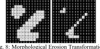
Erosion
It is defined in terms vector subtraction. Let us consider the input image ‘X’ and structuring element ‘B’ then the dilation of ‘X’ w.r.t ‘B’ is given by
(3) The basic effect of erosion operator on a binary or gray image is to erode away (remove) the boundaries of foreground pixels (i.e. the white pixels). Thus areas of foreground pixels shrink in size, and the area of the background pixels increases. With the structuring element ‘B’(2), the effect of this operation is to remove any foreground pixel that is not completely surrounded by other foreground pixels. This operation can be performed on binary images simply by applying a logical AND function.
1) If the input pixel is set to foreground and all its 8 neighbors are also set to foreground, then the pixel remains set to foreground.
2) If the input pixel is set to foreground, but at least one of its 8 neighbor’s is not, the pixel is set to background. 3) Input pixels set to background remain same.
Fig. 9: Boundary Extraction
VII.RESULT
The results of number plate reading obtained by MATLAB simulation and VHDL simulation results of I2C protocol and data storing into memory are presented here.
MATLAB Simulation Results
Number Plate Reading
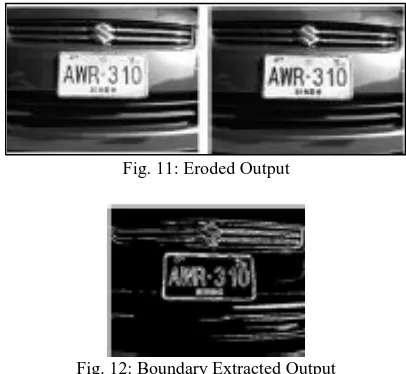
Mathematical Morphology is used to extract the information from an image and it requires input image and structuring element for its Morphological Transformations (like Dilation, Erosion and Boundary Extraction). Initially the input image is dilated and eroded with structuring element ‘B’ (2). Figure 10 is the morphological dilation transformation of input image. Figure 11 is the morphological erosion transformation of input image. Figure 12 is the morphological boundary extraction transformation of input image.
Fig. 11: Eroded Output
Fig. 12: Boundary Extracted Output
The boundary extracted image is then again eroded with different structuring element and output image of erosion is subtracted from the boundary extracted image to remove horizontal lines if any. After removing the horizontal lines “Hole fill” will be done i.e. background pixels which are within the boundary of object will get filled by foreground pixels. The output is shown in figure 13.
Fig. 13: Output Image after Hole Fill
Fig. 14: Output Notepad (Result)
Fig. 15: Pop Up Messages for Matched & Unmatched Cases
Figure 16 shows the MATLAB GUI for reading number plate.
Fig. 16: MATLAB GUI for Reading Number Plate
VIII. VHDL SIMULATION RESULTS
I2C Protocol
I2C protocol is used between image sensor and FPGA to program the image sensor for gain, frame size, frame rate.
1) The VHDL simulation result of 16-Bit Write (last bit of address is ‘0’) Sequence is shown in figure 17. Address of the register is ”10100110” and 16-bit data written into this register address is “1011010011011010”.
2) The 16-bit read (last bit of address is ‘1’) sequence is shown in figure 18.Address of the register is “10110101” and 16-bit data read from this register address is “1101010111011010”.
Fig. 17: 16-Bit Write Sequence
Data Storing into Memory
Into memory it requires 8 clock cycles. In which one clock cycle is to set up a command, 5 clock cycles to set up an address, one clock cycle is to load a data and remaining one clock cycle is to confirm code command.
Fig. 19: VHDL Simulation of Clock Divisor (1:8)
These 8 bus cycles are generated from the input clock. Figure 19 shows the VHDL simulation for the generation of 8 clock cycles from one input clock cycle. Figure 20 shows the VHDL simulation of data storing into memory.
Fig. 20: VHDL Simulation of Data Storing Into Memory
IX. CONCLUSION & FEATURE SCOPE
This paper describes the design and development of an embedded camera with built in image processing. Design is done using the OrCAD 10.0 tool. Algorithms such as number plate reading is implemented in MATLAB. Result of this algorithm is verified by using image processing tool box of MATLAB version R2013a. The I2C protocol is implemented using VHDL for programming the image sensor on FPGA. Its features can be extended by reducing the capture time period and implementing automatic gain control.
The future scope of this is to develop the boards and load any image processing algorithm to configure the FPGA.
REFERENCES
[1] Rafael C. Gonzalez., and Richard E. Woods, ”Digital image processing” Prentice Hall, 2 edition 2001, pp. 523-527, 534-536.
[2] Aptina, (2006), MT9M001: 1/2-Inch Megapixel Digital Image Sensor Die Features,
https://www.aptina.com/products/imagesensors/mt9m001c12stm/, (Nov. 23, 2013).
[3] Xilinx,(2008-2011)’ ”Spartan3A FPGA Family Data Sheet”, http://www.xilinx.com/support/documentation/data sheets/ds529.pdf, (Dec.
11, 2013).
[4] Xilinx, (2003-2010), ”Platform Flash In-System Programmable Configuration PROMs”,http://www.xilinx.com/support/documentation/data
sheets/ds123.pdf, (Dec. 9,2013).
[5] Numonyx, (2007), ”4-Gbit, 8-Gbit, 2112- byte& 1056-word page multiplane architecture, 1.8V or 3V, SLC NAND flash memories”,
http://media.digikey.com/pdf/Data%20Sheets/Numonyx,Intel/NAND04GB2D,08GBxC.pdf, (Dec. 15, 2013).
[6] Texas Instruments, (1999-2013), ”LM3940 1A Low Dropout Regulator for 5V to 3.3V Conversion”, http://www.ti.com/lit/ds/symlink/lm3940.pdf, (Jan. 11,
2014).
[7] On Semiconductor, (2012), ”150 mA, Tri-Mode, LDO Linear Voltage Regulator”,http://www.onsemi.com/pub link/Collateral/NCP4587-D.PDF, (Jan. 11,
2014).
[8] Cypress , (2013), ”EZ-USB R FX2LPTM USB Microcontroller High-Speed USB Peripheral Controller” ,http://www.cypress.com/?docID=45142, (Jan.