FFT Analysis, Simulation of Computational
Model and Netlist Model of Digital Phase Locked
Loop
Richa Soni
Department of Electronics & Communication Engineering Gargi Institute of Science & Technology Bhopal, India
Abstract
The most versatile application for digital phase locked loops is for clock generation and clock recovery in any complex computer architecture like a microprocessor or microcontroller, network processors. Digital Phase locked loops are commonly used to generate timing on chip clocks in high performance mixed signal analog and digital systems. Most of the systems employ digital PLL mainly for synchronization, skew and jitter optimization. Because of the need of high speed circuitry there is a need of PLL. Mostly communication, wireless systems, RF Processors operate in Gigahertz range; there is a necessity of PLL that too digital which operate in high order frequencies. Digital PLL is a mixed signal integrated circuit and presented work focuses on design and analysis of efficient digital phase locked loops for clock generation using 50nm SPICE models. A computational model is designed using MATLAB and also SPICE scripting is done using suitable simulation engine for the same. The presented design Digital PLL performs the function of mainly generating a clock signal also consists of design of sub circuits and systems like phase detector, loop filters and voltage controlled oscillators. A detailed FFT analysis is also presented with parameters magnitude, phase and group delay calculated for each sub circuits and systems. The results of DPLL designed using proper optimization method is also compared with traditional method.
Keywords: Digital PLL, SPICE, VCO, Phase Detector, FFT, Loop filters
________________________________________________________________________________________________________
I. INTRODUCTION
Digital Phase locked loop is a mixed signal analog integrated circuit. Digital PLL is the heart of many communication as well as electronic systems. Mostly a higher lock PLL range with lesser locking time and should have tolerable phase noise. The most versatile application of a digital PLL is for clock generation or synchronization, clock recovery, communication systems and frequency synthesizers. In high performance digital systems like processors digital PLL or DPLL are commonly used to generate well timed on chip clock signals. Modern RF circuits or wireless mobile communication systems use PLL for synchronization, timing based synthesis, skew and jitter reduction. Digital PLL is extensively used in advanced communication systems, electronic and medical instrumentation systems. The PLLs are an integrated part of larger circuits on a single chip.
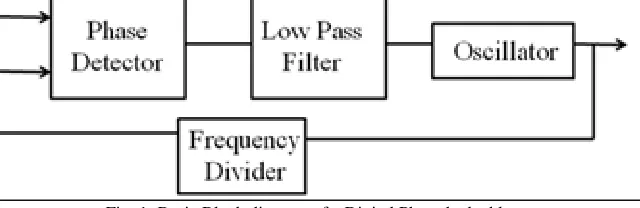
A simple PLL consists of namely four to five integrated blocks. They are phase frequency detector, charge pump, Loop filters, and voltage controlled oscillator and frequency dividing circuits.
Fig. 1: Basic Block diagram of a Digital Phase locked loop
II. DESIGNING A DIGITAL PLL
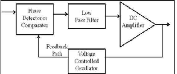
A PLL is a closed-loop feedback system that sets fixed phase relationship between its output clock phase and the phase of a reference clock. A PLL is capable of tracking the phase hanges that falls in this bandwidth of the PLL. A PLL also multiplies a low-frequency reference clock CKref to produce a high-frequency clock CKout this is known as clock synthesis. A PLL has a negative feedback control system circuit. The main objective of a PLL is to generate a signal in which the phase is the same as the phase of a reference signal. This is achieved after many iterations of comparison of the reference and feedback signals. In this lock mode the phase of the reference and feedback signal is zero. After this, the PLL continues to compare the two signals but since they are in lock mode, the PLL output is constant. A basic PLL is a negative feedback system that receives an incoming oscillating signal and generates an output waveform that exerts the same phase, frequency relationship as the input signal. This is achieved by constantly comparing the phase of output signal to the input signal with a phase frequency detector (PFD).
The Phase frequency Detector (PFD) is one of the main parts in PLL circuits. It compares the phase and frequency difference between the reference clock and the feedback clock. Depending upon the phase and frequency deviation, it generates two output signals UP and DOWN. The Charge Pump (CP) circuit is used in the PLL to combine both the outputs of the PFD and give a single output. The output of the CP circuit is fed to a Low Pass Filter (LPF) to generate a DC control voltage. The phase and frequency of the Voltage Controlled Oscillator (VCO) output depends on the generated DC control voltage. If the PFD generates an up signal, the error voltage at the output of LPF increases which in turn increase the VCO output signal frequency. On the contrary, if a Down signal is generated, the VCO output signal frequency decreases. The output of the VCO is then fed back to the PFD in order to recalculate the phase difference, and then we can create closed loop frequency control system.
III. PLL ARCHITECTURE
In general a PLL consists of five main blocks:
1) Phase Detector or Phase Frequency Detector (PD or PFD) 2) Charge Pump (CP)
3) Low Pass Filter (LPF)
4) Voltage Controlled Oscillator (VCO) 5) Divide by N Counter
Fig. 2: A generic architecture of Digital PLL
Phase frequency Detector:
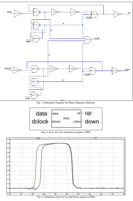
The phase frequency detector is one of the main integral parts of PLL circuits. It compares the phase and frequency difference between the reference clock and feedback clock. Depending upon the phase and frequency deviation it generates two output signals Up and Down. If there is a phase difference between the two signals, it will generate UP or DOWN synchronized signals. When the reference clock rising edge leads the feedback input clock rising edge UP signal goes high while keeping “DOWN” signal low. On the other hand if the feedback input clock rising edge leads the reference clock rising edge “DOWN” signal goes high and “UP” signal goes low. Fast phase and frequency acquisition PFDs are generally preferred over traditional PFD.
Fig. 3: Schematic Diagram for Phase frequency Detector
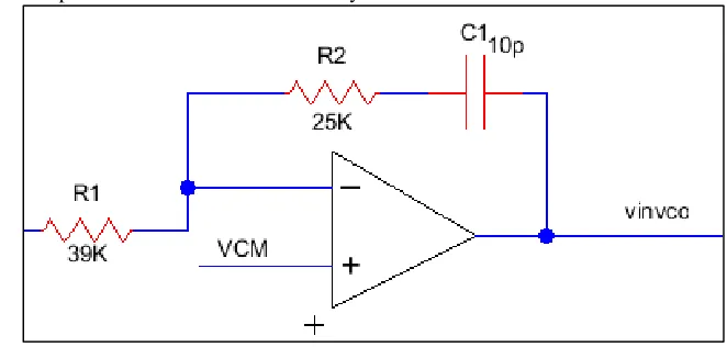
Charge Pump and Loop Filter:
Charge pump circuit is an important block of the whole PLL system.
Fig. 6: Basic Charge Pump Loop Filter using Opamp
It converts the phase or frequency difference information into a voltage, used to tune the VCO. Charge pump circuit is used to combine both the outputs of the PFD and give a single output which is fed to the input of the filter.
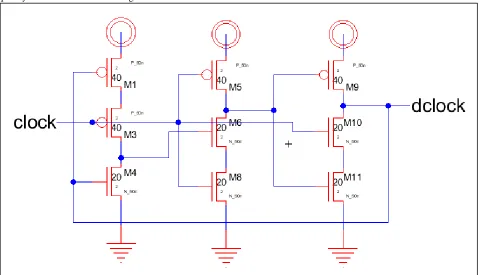
Voltage Controlled Oscillator:
An oscillator is an autonomous system which generates a periodic output without any input.The most popular type of the VCO circuit is the current starved voltage controlled oscillator
(CSVCO). Here the number of inverter stages is varied, generically used with 21 stage with simple inverter or current starved configurations
Frequency Divider:
The output of the VCO is fed back to the input of PFD through the frequency divider circuit. The frequency divider in the PLL circuit forms a closed loop. It scales down the frequency of the
VCO output signal. A simple flip flop (FF) acts as a frequency divider circuit. The schematic of a simple divider based divide by 2 frequency circuit is shown in the Figure 8
Fig. 8: Schematic view for frequency divider network
IV. DESIGN AND SYNTHESIS OF DPLL
The schematic level design entry of the circuits is carried out in the Electric CAD VLSI Design Environment. The structure of the DPLL is designed in Electric CAD using 50 nm SPICE models for CMOS. In order to analyze the performances, these circuits are simulated in the LTSPICE simulator of Level 3 or 4 BSIM SPICE CAD. Different performance indices such as phase,group delay and corresponding magnitude are measured in this environment. Transient parametric sweep and phase analyses are carried out in this work to find out the performances of the circuit. The optimization of the current starved VCO circuit, the scale factor for transistor sizing is found out using the LTSpice environment.
Following Design procedure is adopted for the presented design 1) VCO Design
2) PFD Loop Design
3) Frequency Divider Circuit
4) Loop Filter and Charge Pump Design 5) Assembling all subunits in a single design 6) Carry out transient analysis
7) FFT analysis
V. SIMULATION RESULTS
Fig. 8: Schematic for VCO Linear analog PLL
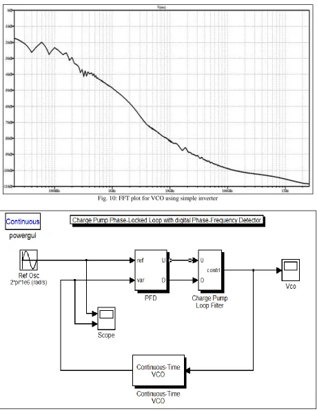
Fig. 10: FFT plot for VCO using simple inverter
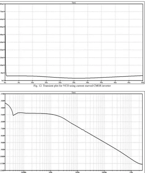
Fig. 12: Transient plot for VCO using current starved CMOS inverter
Fig. 14: DPLL topology 1 using RC as loop filter and Charge pump
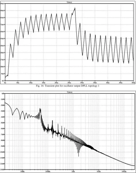
Fig. 16: Transient plot for oscillator output DPLL topology 1
Fig. 18: DPLL topology 2 using Opamp as loop filter and Charge pump
Fig. 21: FFT Plot for Oscillator output DPLL topology 2
Fig. 23: Transient plot for Vdata and Vclock in DPLL topology 3
Fig. 25: FFT Plot for Oscillator output DPLL topology 2
Fig. 27: Schematic of DLL Clock generator
Fig. 28: Schematic waveform of DLL Clock generator
VI. FFT RESULTS
Table – 1
VII. CONCLUSION
In this paper presented DPLL works with better locking times, the digital PLL consumes low power as designed with 50 nm CMOS technology, the transient analysis mainly depends on the type of the PFD architecture used and parasitic parameters utilized for charge pumps and loop filters. So by properly choosing VCO architecture, PFD design and adjusting the charge pump configurations. The efficiency of the overall design also depends on the reduction of transistor sizes which is 50nm.
REFERENCES
[1] Dian Huang, Ying Qiao, “A fast locked all digital phase locked loop for dynamic frequency scaling”,
[2] Moon Seok Kim, Yong Bin Kim, Kyung Ki Kim, “All digital phase locked loop with local passive interpolation time to digital converter based on tristate inverter ” IEEE transactions 2012R.E. Best, “Phase Locked Loops Design, Simulation and Applications,” McGraw-HillPublication, 5th Edition, 2003. [3] Dan H. Wolaver, “Phase Locked Loop Circuit Design,” Prentice Hall Publication, 1991.
[4] R.J.Baker, H.W.Li, and D.E.Boyce, “CMOS Circuit Design, Layout, and Simulation,” IEEE Press Series on Microelectronic Systems, 2002.
[5] S. M. Shahruz, “Novel phase-locked loops with enhanced locking capabilities,” Journal of Sound and Vibration, Vol. 241, Issue 3, 29 March 2001, Pages 513-523.
[6] B. Razavi, “Design of Analog CMOS Integrated Circuits,” Tata McGraw Hill Edition,2002
[7] M.Mansuri, D.Liu, and C.K.Yang, “Fast Frequency Acquisition Phase Frequency Detector for GSamples/s Phase Locked Loops,” IEEE Journal of Solid State Circuit, Vol. 37, No. 10, Oct., 2002.
[8] Youngshin Woo, Young Min Jang and Man Young Sung, “Phase-locked loop with dual phase frequency detectors for high-frequency operation and fast acquisition,” Microelectronics Journal, Vol. 33, Issue 3, March 2002, Pages 245-252.
[9] Quan Sun, Yonguang Zhang, Christine Hu-Guo, Kimmo Jaaskelainen and Yann Hu, “A fully integrated CMOS voltage regulator for supply-noise-insensitive charge pump PLL design,” Miroelectronics Journal, Vol. 41, Issue 4, April 2010, Pages 240-246
[10] S.J.Li, and H.H.Hsieh,” A 10 GHz Phase-Locked Loop with a Compact Low-Pass Filter in 0.18 µm CMOS Technology”, IEEE Microwave and Wireless Components Letters, VOL. 19, NO. 10, OCTOBER 2009
[11] H.Janardhan, and M.F.Wagdy “Design of a 1GHz Digital PLL Using 0.18 µm CMOS Technology,” IEEE Proc. of the Third International Conference on Information Technology, 2006.
[12] S.M.Kang, and Y.Leblebici, “CMOS Digital Integrated Circuits: Analysis and Design,” McGraw-Hill Publication, 3 rd Edition, 2003.