http://www.sciencepublishinggroup.com/j/am doi: 10.11648/j.am.20180704.13
ISSN: 2327-2503 (Print); ISSN: 2327-252X (Online)
Role of [Cu]/[In] Molar Ratio in Controlling Structural,
Morphological and Optical Properties of Sprayed CuInS
2
Thin Films
Mazabalo Baneto
1, *, Damgou Mani
Kongnine
1, Krishnasamy Ravichandran
2, Donafolgo Soro
3,
Koffi Sagna
1, Kossi Napo
11
Department of Physics, University of Lomé, Lomé, Togo
2
Post Graduate and Research Department of Physics, AVVM Sri Pushpam College (Autonomous), Thanjavur, India
3
Department of Sciences and Technology, High Normal School of Abidjan, Abidjan, Ivory Coast
Email address:
*
Corresponding author
To cite this article:
Mazabalo Baneto, Damgou ManiKongnine, Krishnasamy Ravichandran, Donafolgo Soro, Koffi Sagna, Kossi Napo. Role of [Cu]/[In] Molar Ratio in Controlling Structural, Morphological and Optical Properties of Sprayed CuInS2 Thin Films. Advances in Materials.
Vol. 7, No. 4, 2018, pp. 111-117. doi: 10.11648/j.am.20180704.13
Received: October 25, 2018; Accepted: November 10, 2018; Published: December 18, 2018
Abstract:
CuInS2 thin films were deposited by chemical spray pyrolysis from aqueous solutions containing CuCl2, InCl3 andthiourea at substrate temperature of 300°C and annealed at 500°C in air. [Cu]/[In] molar ratio was varied from 0.8 to 1.4 in precursor solution. The influence of [Cu]/[In] molar ratio on structural, morphological and optical properties of CuInS2 thin
films was investigated. X-ray diffraction analysis shows that all the films have chalcopyrite structure with the preferential orientation along (112) plane. CuInS2 films with indium excess have poor crystallinity and consist of large quantity of small
particles while copper-rich films exhibit good crystallinity with large grains. The best film crystallinity is obtained for [Cu]/[In] = 1.2. The scanning electron microscopy and atomic force microscopy images indicated that [Cu]/[In] molar ratio has a strong influence on the microstructure and surface morphology of the films. It was observed that films obtained with [Cu]/[In] ratio of 0.8 are porous. But films surface became gradually dense with increase in [Cu]/[In] molar ratio. As consequence films roughness decreased from 236.12 nm to 110.30 nm. Optical analysis shows that all the films have good absorbance in the visible. The optical absorbance of films is found to increase with increase in [Cu]/[In] molar ratio.
Keywords:
Thin Film, CuInS2, Molar Ratio, Spray Pyrolysis1. Introduction
The conversion of sunlight directly into electricity using the photovoltaic properties of suitable materials is perfect energy conversion process [1]. Photovoltaic energy to be widely used, the key issue is higher efficiency of energy conversion, low-cost materials and low-cost manufacturing process. In recent years, the critical issues of global warming and energy-resource crises have driven scientists, engineers and technologists to develop thin-films photovoltaic devices, which directly convert sunlight into electricity mainly by semiconductor absorber layers [2], such as CdTe [3], CdSe
[4], PbS [5], CuInSe2 [6], CuInS2 [7], CuIn (Se, S)2 [8],
CuInxGa1-xSe2 [9] and Cu (In, Ga) (Se, S)2 [10]. Among
these, the ternary chalcopyrite semiconductor CuInS2 (CIS)
has received intense attention for its potential higher conversion efficiency of 30% [11], utilising low-cost and environmentally friendly materials [12]. It exhibits high absorption coefficient of more than 104 cm-1 [13] and direct optical band gap of about 1.5 eV [14], which matches well with the solar spectrum. In addition, CuInS2 exhibts
influenced mainly by the qualities of CuInS2 thin films.
Hence, many studies have focused on finding the correlation between its preparation methods and the resulting properties in structure, morphology and photo-electricity. Moreover, the deposition temperature and [Cu]/[In] molar ratio play a crucial role on the properties of CuInS2 thin films. In our
previous work [20], we studied the effects of growth temperature on the properties of spray deposited CuInS2 thin
films for photovoltaic applications.
The main purpose of the present work is to prepare single-phase CuInS2 thin films by spray pyrolysis method. These
films are deposited from mixed solutions with different chemical compositions ([Cu]/[In] ratios) and heated-treated under room air at 500°C for 1h. The preparative parameters were optimized and the influence of the [Cu]/[In] molar ratio on different properties of CuInS2 thin films was investigated.
2. Experimental Details
Spray pyrolysis deposited CuInS2 thin films were obtained
from an aqueous solution containing CuCl2, InCl3 and (CS
(NH2)2). In the present study, [Cu]/[In] molar ratio in the
precursor solution was varied in the range of 0.8–1.4. First, a solution of CuCl2 and CS (NH2)2 was mixed, which was
followed by the addition of InCl3 solution. The solvent was a
mixture of deionized water and ethanol with the ratio of (4:1). Previous studies have shown that 300°C was the optimal deposition temperature [20]. Thus, a solution of a total amount of 50 ml was sprayed onto pre-heated glass substrates at 300°C. Compressed ambient air was used to atomize the solution at the pressure of 2 bar. Initially the substrates were successively cleaned in an ultrasound bath, using ethanol and distilled water, and were further dried in air. Post-deposition annealing was done for 1h in air at 500°C.
The crystalline structure of the samples was studied by XRD analysis using a Bruker D8 Discover Advanced
films was determined by energy dispersive X- ray spectroscopy (EDX, with 15 kV operating voltage).
3. Results and Discussion
3.1. Structural Analysis
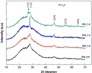
The structural properties of the films were investigated using XRD measurement. Figure 1 shows the XRD spectra of CuInS2 thin films derived from different [Cu]/[In] ratios. The
protruding background in the range of 15 to 40° originates from the diffraction of glass substrate. The diffraction peaks can be assigned for CuInS2 planes (112), (200), (204) (312)
and (400), respectively (JCPDS 65 – 1572). It is confirmed that all the films have polycrystalline chalcopyrite CuInS2
structure with the preferred orientation along (112) plane. It can be seen that the intensity of the peak (112) increases with increase in [Cu]/[In] ratio up to 1.2. For further increase in [Cu]/[In] ratio, the intensity of the peak (112) decreases and we remarked the appearance of an additional phase of Cu2S
(Figure 1 (CIS_1.4)). Hence, the [Cu]/[In] ratio in the solution can drastically affect the crystallinity of CIS films. The crystallinity of the film with indium excess is poor (Figure 1 (CIS_0.8)), which may be ascribed to the intrinsic defects of indium in copper sites (InCu) and indium
interstitials (Ini) [25]. On the other hand, the improvement of
crystallinity with increase of the [Cu]/[In] ratios from 0.8 to 1.2 can be attributed to higher mobility of copper ions [26].
As seen in Figure 1, the preferential orientation of the (112) peak do not increase monotonously with [Cu]/[In] ratios. The near stoichiometric CuInS2 film with [Cu]/[In] =
1.2 has the optimum value of the preferential orientation. We noticed that when [Cu]/[In] ratio is higher than 1.2, the crystallinity of the film decreases as a consequence of the crystal structure deformation and/or recrystallization. This is confirmed by the appearance of the second phase Cu2S with
Figure 1. X-ray powder diffraction patterns of samples.
The average crystallite sizes corresponding to the prominent peak (112) was calculated using Scherrer formula:
0.9
where β is the observed angular width at half maximum intensity (FWHM) of the peak, λ is the X-ray wavelength (1.5406 Å for CuKα1) and θ is the Bragg’s angle. The
different crystallite sizes obtained for different [Cu]/[In] ratios are reported in table 1. It can be seen that the crystallite sizes varied with [Cu]/[In] molar ratios. The largest crystallite size is obtained with [Cu]/[In] = 1.2 confirming the good crystallinity of the films.
Table 1. Crystallite sizes and average roughness of CuInS2 films with different [Cu]/[In] molar ratios.
Sample name Crystallite sizes (nm) Roughness (nm)
CIS_0.8 8.05 236.12
CIS_1.0 9.72 202.75
CIS_1.2 25.40 110.30
CIS_ 1.4 17. 95 143. 82
3.2. Compositional Analysis
The stoichiometric ratio of [Cu]/[In] is an important factor in CuInS2 films. By controlling the ratio of composition
element, n-type or p-type CuInS2 can be adjustedeasily [27].
Indium-rich films may lead to the formation of n-type CuInS2
film, while copper-rich may result in p-type CuInS2. Figure 2
compares the [Cu]/[In] ratio in the precursor solution and the [Cu]/[In] ratio in the film. The [Cu]/[In] ratios in the deposited films were calculated from the EDX results (Table 2). It is observed that the [Cu]/[In] ratio in film increases monotonously with the increase of [Cu]/[In] ratio in the precursor solution and always higher than that in precursor
solution. As the [Cu]/[In] ratio in the mixed solution was varied from 0.8 to 1.4, [Cu]/[In] ratio in the film changed from 0.9 to 1.9. This indicates that there was more Cu in the film than in the precursor solution. It may be due to the fact that, Copper has higher reactivity compared to indium.
Table 2. EDX results showing atomic percentage of elements in CuInS2 films.
Sample
name Cu (%) In (%) S (%)
Cu /In (in film)
Cu / In (in solution)
CIS_0.8 26.18 29.42 44.40 0.9 0.8
CIS_1.0 30.10 26.05 43.85 1.2 1.0
CIS_1.2 35.62 21.60 42.78 1.7 1.2
CIS_1.4 38.92 21.02 41.44 1.9 1.4
Figure 2. [Cu]/[In] ratio in the film as a function of [Cu]/[In] ratio in precursor solution.
3.3. Surface Morphology
The SEM images of CuInS2 thin films deposited at
Figure 3. SEM images of CuInS2 films with different [Cu]/[In] molar ratios: (a) CIS_0.8; (b) CIS_1.0; (c) CIS 1.2; (d) CIS_1.4.
All the films are relatively homogenous, smooth and adherent to the substrate. It can be seen from the AFM images (Figure 4) that, [Cu]/[In] ratio has a strong influence on the microstructure and surface morphology of the films. Films deposited from precursor with [Cu]/[In] ratio of 0.8 (Figure 4 (a)) are very porous and consist of large quantity of small particles which are less than 250 nm in size. When [Cu]/[In] ratio increases, the film surface becomes dense ( Figure 3 (b, c and d)) and the grain size also increases (Figure 4 (b, c and d)). The agglomeration of particles into
Figure 4.AFM images of CuInS2 films with different [Cu]/[In] molar ratios: (a) CIS_0.8; (b) CIS_1.0; (c) CIS 1.2; (d) CIS_1.4.
3.4. Optical Properties
Figure 5 shows the optical absorbance spectra of CIS films in the wavelength range of 300-1200 nm. It can be observed that all the films exhibit good absorbance in the visible. In addition, it can be also seen that the absorbance increases with increase in [Cu]/[In] ratio. This can be explained, on the one hand by the fact that with increasing in [Cu]/[In] ratio films thickness also increases leading to higher absorbance. On the other hand, it can be due to the fact with increasing in [Cu]/[In] ratio, films exhibit good crystallinity as discussed in XRD results. It is well known that good crystallinity is a key factor in thin film optical absorbance. But in the present
study, in contrast, we remarked that although films obtained with [Cu]/[In] = 1.2 exhibit good crystallinity compared to those obtained with [Cu]/[In] = 1.4, they present lower absorbance. This can be interpreted by the poor crystallinity or deviation from stoichiometry that gives rise to defect states and thus induce smearing of absorption edge. On the other hand, a possible reason for this phenomenon can be carrier degeneracy in CuInS2 films due to continuous
distribution of defect states. For example, copper and indium vacancies (VCu and VIn), substitutional copper indium sites
(CuIn) and the defects pairs such as (2VCu- + InCu2+) and
Figure 5. Optical absorbance spectra of the CuInS2 films with different [Cu]/[In] molar ratios.
4. Conclusion
Sprayed CuInS2 thin films have been deposited from
aqueous solutions containing CuCl2, InCl3 and thiourea with
different [Cu]/[In] molar ratios. The effect of molar ratio on structural, morphological and optical properties of CuInS2
have been investigated. The X-ray diffraction analysis shows that all the films have polycrystalline chalcopyrite CuInS2
structure with the preferred orientation along (112) plane. Films with indium excess have poor crystallinity while Copper-rich films exhibit good crystallinity. The largest crystallite size is obtained for [Cu]/[In] = 1.2. The surface morphology study reveals that all the films are homogenous, smooth and adherent to the substrate. Copper-rich films had well developed grains, whereas indium-rich films exhibited poorly grown grains. The optical analysis shows that all the films exhibit good absorbance in the visible.
References
[1] Park MS, Han SY, Bae EJ, Lee TJ, Chang CH, Ryu SO, Synthesis and characterization of polycrystalline CuInS2 thin
films for solar cell devices at low temperature processing conditions, Curr Appl Phys 2010; 10: S 379–82.
[2] I. Konovalov, Material requirements for CIS solar cells, Thin Solid Films 451– 452 (2004) 413–419.
[3] R. S. Singh, V. K. Rangari, S. Sanagapalli, V. Jayaraman, S. Mahendra, V. P. Singh, Nano structured CdTe, CdS and TiO2
for thin film solar cell applications, Sol. Energy Mater. Sol. Cells 82 (2004) 315–330.
[4] C. Lévy-Clément, R. Tena-Zaera, M. A. Ryan, A. Katty, G. Hodes, CdSe - sensitized p-CuS CN/nanowire n- ZnO heterojunctions, Adv. Mater. 17 (2005) 1512–1515.
processes, Thin Solid Films 431–432 (2003) 116–121. [9] M. Venkatachalam, M. D. Kannan, S. Jayakumar, R.
Balasundaraprabhu, A. K. Nandakumar, N. Muthukumarasamy, CuInxGa1xSe2 thin films prepared by
electron beam evaporation, Sol. Energy Mater. Sol. Cells 92 (2008) 571–575.
[10] J. Palm, V. Probst, F. H. Karg, Second generation CIS solar modules, Sol. Energy 77 (2004) 757–765.
[11] J. M. Meese, JC Manthuruthil, D. R. Locker, CuInS2 Diodes
for solar energy conversion, Bull Am Phys Soc 1975; 20:696– 707.
[12] P. Guha, S. Gorai, D. Ganguli, S. Chaudhuri, Ammonia -mediated wet chemical synthesis of CuInS2 Mater Lett 2003;
57:1786–1791.
[13] W. J. Tsai, C. H. Tsai, C. H. Chang, J. M. Ting, R. R. Wang, Addition of Na into CuInS2 thin film via co- evaporation Thin
Solid Films 2010; 519: 1712–1716.
[14] J. P. Xiao, Y. Xie, R. Tang, Y. T. Qian, Synthesis and Characterization of Ternary CuInS2 Nanorods Via a
Hydrothermal Route, J Solid State Chem 2001; 161: 179–183. [15] Y. Chen, X. He, X. Zhao, M. Song, X. Gu, Preparation and
characterization of copper indium disulfide films by facile chemical method, Mater. Sci. Eng. B 139 (2007) 88–94. [16] K. Siemer, J. Klaer, I. Luck, J. Bruns, R. Klenk, D. Braünig,
Efficient CuInS2 solar cells from a rapid thermal process
(RTP), Sol. Energy Mater. Sol. Cells 67 (2001) 159– 166. [17] R. Scheer, I. Luck, M. Kanis, M. Matsui, T. Watanabe, T.
Yamamoto, Incorporation of the doping elements Sn, N, and P in CuInS2 thin films prepared by co-evaporation, Thin Solid
Films 392 (2001) 1.
[18] H. J. Muffer, C. H. Fischer, K. Diesner, LGAR—A novel thin-film technology for sulfides, Sol. Energy Mater. Sol. Cells 67 (2001) 121.
[19] J. A. Hollingsworth, K. K. Banger, M. H. C. Jin, Single source precursors for fabrication of I-III-VI2 thin-film solar cells via spray CVD), Thin Solid Films 431 (2003) 63.
[20] M. Baneto, A. Enesca, C. Mihoreanu, Y. Lare, K. Jondo, K. Napo, A. Duta, Effects of the growth temperature on the properties of spray deposited CuInS2 thin films for
photovoltaic applications. Ceramics International 41 (3), 4742-4749 (2015).
[21] Y. B. He, A. Polity, H. R. Alves, I. O¨ sterreicher, W. Kriegseis, D. Pfisterer, B. K. Meyer, M. Hardt, Structural and optical characterization of RF reactively sputtered CuInS2 thin
[22] H. M. Pathan, C. D. Lokhande, Chemical deposition and characterization of copper indium disulphide thin film, Appl. Surf. Sci. 239 (2004) 11.
[23] M. Baneto, A. Enesca, Y. Lare, K. Jondo, K. Napo, A. Duta, Effect of precursor concentration on structural, morphological and opto-electric properties of ZnO thin films prepared by spray pyrolysis Ceramics International 40 (2014) 8397–8404. [24] A. Enesca, M. Baneto, D. Perniua, L. Isaca, C. Bogatu, A.
Duta, 7. Solar-activated tandem thin films based on CuInS2,
TiO2 and SnO2 in optimized wastewater treatment processes,
Applied Catalysis B: Environmental 186 (2016) 69–76. [25] J. H. Schon, E. Bucher, Characterization of Intrinsic Defect
Levels in CuInS2, Phys. Status Solidi 171 (1999) 511.
[26] M. Krunks, V. Milli, O. Bijakina, H. Rebane, Composition and structure of CuInS2 films prepared by spray pyrolysis, Thin
Solid Films 361 (2000) 61.
[27] G. C. Park, H. D. Chung, C. D. Kim, H. R. Park, W. J. Jeong, J. U. Kim, H. B. Gu, K. S. Lee, Photovoltaic characteristics of CuInS2/CdS solar cell by electron beam evaporation, Solar
Energy Materials and Solar Cells 49 (1997) 365.
[28] R. Klenk, T. Walter, H. W. Schock, A model for the successful growth of polycrystalline films of CuInSe2 by multisource
physical vacuum evaporation, Adv. Mater. 5 (1993) 114. [29] S. B. Zhang, S. H. Wei, A. Zuger, Defect physics of the
CuInSe2 chalcopyrite semiconductor Phys. Rev. 57 (1997)
![Figure 3. SEM images of CuInS2 films with different [Cu]/[In] molar ratios: (a) CIS_0.8; (b) CIS_1.0; (c) CIS 1.2; (d) CIS_1.4](https://thumb-us.123doks.com/thumbv2/123dok_us/8469717.1710904/4.595.71.528.84.458/figure-sem-images-cuins-films-different-molar-ratios.webp)
![Figure 4. AFM images of CuInS2 films with different [Cu]/[In] molar ratios: (a) CIS_0.8; (b) CIS_1.0; (c) CIS 1.2; (d) CIS_1.4](https://thumb-us.123doks.com/thumbv2/123dok_us/8469717.1710904/5.595.69.535.71.594/figure-afm-images-cuins-films-different-molar-ratios.webp)
![Figure 5. Optical absorbance spectra of the CuInS2 films with different [Cu]/[In] molar ratios](https://thumb-us.123doks.com/thumbv2/123dok_us/8469717.1710904/6.595.47.284.121.320/figure-optical-absorbance-spectra-cuins-films-different-ratios.webp)
