University of Pennsylvania
ScholarlyCommons
Publicly Accessible Penn Dissertations
2018
Microlamination Based Lumped And Distributed
Magnetic Mems Systems Enabled By
Through-Mold Sequential Multilayer Electrodeposition
Technology
Yuan Li
University of Pennsylvania, [email protected]
Follow this and additional works at:https://repository.upenn.edu/edissertations Part of theNanoscience and Nanotechnology Commons
This paper is posted at ScholarlyCommons.https://repository.upenn.edu/edissertations/2965 For more information, please [email protected].
Recommended Citation
Li, Yuan, "Microlamination Based Lumped And Distributed Magnetic Mems Systems Enabled By Through-Mold Sequential Multilayer Electrodeposition Technology" (2018).Publicly Accessible Penn Dissertations. 2965.
Microlamination Based Lumped And Distributed Magnetic Mems
Systems Enabled By Through-Mold Sequential Multilayer
Electrodeposition Technology
Abstract
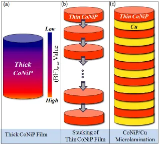
Microfabricated magnetic MEMS components such as permanent micromagnets and soft magnetic structures are key enablers in various lumped and distributed systems such as energy harvesters, magnetometers, biomagnetic filters, and electromagnetic micromotors. The unique functionalities of such systems often require designers to controllably scale the relevant dimensions of a device relative to the characteristic length of a targeted application. We demonstrate in this dissertation that the developed Microlamination Technology could create two-dimensional uniform- or dual- height monolithic metallic structures with additional
deterministic structural and compositional complexities along thickness direction, suitable to facilely and flexibly fabricate both lumped and distributed magnetic MEMS systems at a designer's will. The utility of the Microlamination Technology is further validated through the realization of two exemplary systems based on this technology:
(i) A lumped system of laminated permanent micromagnets. Microfabricated permanent magnets possessing a multilayer structure enabled by the Microlamination Technology that preserves the high energy density of thinner magnetic films, while simultaneously reducing average residual stress of the films and achieving a significant thickness are presented. The key to retain the superior magnetic properties of thin films in thick laminations is the low interface roughness between the layers, which in turn improves the coercivity of the micromagnets.
(ii) A distributed system of a bi-stable vertical magnetic actuator with non-contact latching. The utilization of the Microlamination Technology translates the structural periodicity (multilayer) into magnetic-field-pattern periodicity, which in turn enables the bi-stability of the microsystem and leads to the defined latching behavior. The latching mechanism is solely based on the magneto-static interaction without the need of a mechanical stop. No external energy is needed in the latching positions. This vertical bi-stable actuator could have potential applications as valves in micro-fluidic controls, and as integral parts of micro-mirrors in optical applications.
Degree Type Dissertation
Degree Name
Doctor of Philosophy (PhD)
Graduate Group
Electrical & Systems Engineering
First Advisor Mark G. Allen
Keywords
Actuator, Electrodeposition, Magnetic, MEMS, Microfabircation, Multilayer
Subject Categories
Engineering | Nanoscience and Nanotechnology
MICROLAMINATION BASED LUMPED AND DISTRIBUTED MAGNETIC MEMS SYSTEMS
ENABLED BY THROUGH-MOLD SEQUENTIAL MULTILAYER ELECTRODEPOSITION
TECHNOLOGY
Yuan Li
A DISSERTATION
in
Electrical and System Engineering
Presented to the Faculties of the University of Pennsylvania
in
Partial Fulfillment of the Requirements for the
Degree of Doctor of Philosophy
2018
Supervisor of Dissertation
____________________
Dr. Mark G. Allen Alfred Fitler Moore Professor
Department of Electrical and System Engineering
Graduate Group Chairperson
____________________
Dr. Alejandro Riberio Associate Professor
Department of Electrical and System Engineering
Dissertation Committee
Dr. Cherie Kagan Stephen J. Angello Professor; Department of Electrical
and System Engineering
Dr. Kevin Turner Professor; Department of Mechanical Engineering
and Applied Mechanics
MICROLAMINATION BASED LUMPED AND DISTRIBUTED MAGNETIC MEMS SYSTEMS
ENABLED BY THROUGH-MOLD SEQUENTIAL MULTILAYER ELECTRODEPOSITION
TECHNOLOGY
COPYRIGHT
2018
Yuan Li
This work is licensed under the Creative Commons Attribution- NonCommercial-ShareAlike 3.0 License
To view a copy of this license, visit
iii Dedication
iv
ACKNOWLEDGMENT
This Ph.D. thesis could not be able to be accomplished without the gracious supports and
helps from lots of people. I would like to use this opportunity to say thank you.
First and foremost, it is my Ph.D. advisor Dr. Mark G. Allen, who not only leads me to
the finish of a degree, but more importantly, taught me how to critically think and
creatively solve problems. These precious skill sets would benefit me far beyond my
graduate student life, influencing the rest of my career.
Secondly, I would like to thank Drs. Cherie Kagan, Kevin Turner, and David Issadore for
their gracious supports and participation in my thesis reading committee members.
Thirdly, I would like to thank MicroSensors and MicroActuators (MSMA) group
members both at Georgia Institute of Technology and University of Pennsylvania, in
particular, Dr. Xuehong 'Shannon' Yu who introduced me to this group; Drs. Florian
Herrault, Jooncheol Kim, Minsoo Kim and Ms. Melissa Tsang for the countless
knowledge pass-down in the field of MEMS and microfabrication; Dr. Brock Peterson
for his help and broad knowledge in the field of magnetism and laser microprocessing;
Mr. Richard Shafer and Dr. Jungkwun 'JK' Kim for equipments design, setup and
administrative work, especially for their helps in building the electroplating system at
Penn. I would also like to thank my peers, Dr. Wen Shen, Mr. Mike Synodis, Mr.
Chenpeng Huang, Ms. Didi She, Mr. Akshay Ananthakrishnan, Ms. Lin Du, Ms. Naixin
Song, and Mr. Tao Zhang for various technical discussion spanning multiple engineering
v
John Russell and Ms. Purnima Sharma for their administrative supports. Most
importantly, I cherish all the friendships from previous and current members of the
research group.
Also, I would also like to thank the trainers and staff members in Singh Center for
Nanotechnology (SCN) at Penn and Institute for Electronics and Nanotechnology (IEN)
at Georgia Tech. In particular, Mr. Charles 'Charlie' Veith at Penn for timely lab supplies
critical to meet the deadlines of various projects. I would like to thank Mr. Steve
Szewczyk and Mr. Liyan Wu for the assistance on XRD measurement, and Dr. Yijie
Jiang for the assistance on triboindenter.
Last but not least, I am very grateful for the love and support of my family: my wife, my
vi
ABSTRACT
MICROLAMINATION BASED LUMPED AND DISTRIBUTED MAGNETIC MEMS
SYSTEMS ENABLED BY THROUGH-MOLD SEQUENTIAL MULTILAYER
ELECTRODEPOSITION TECHNOLOGY
Yuan Li
Mark G. Allen
Microfabricated magnetic MEMS components such as permanent micromagnets and soft
magnetic structures are key enablers in various lumped and distributed systems such as
energy harvesters, magnetometers, biomagnetic filters, and electromagnetic micromotors.
The unique functionalities of such systems often require designers to controllably scale
the relevant dimensions of a device relative to the characteristic length of a targeted
application. We demonstrate in this dissertation that the developed Microlamination
Technology could create two-dimensional uniform- or dual- height monolithic metallic
structures with additional deterministic structural and compositional complexities along
thickness direction, suitable to facilely and flexibly fabricate both lumped and distributed
magnetic MEMS systems at a designer's will. The utility of the Microlamination
Technology is further validated through the realization of two exemplary systems based
on this technology:
(i) A lumped system of laminated permanent micromagnets. Microfabricated permanent
magnets possessing a multilayer structure enabled by the Microlamination Technology
vii
reducing average residual stress of the films and achieving a significant thickness are
presented. The key to retain the superior magnetic properties of thin films in thick
laminations is the low interface roughness between the layers, which in turn improves the
coercivity of the micromagnets.
(ii) A distributed system of a bi-stable vertical magnetic actuator with non-contact
latching. The utilization of the Microlamination Technology translates the structural
periodicity (multilayer) into magnetic-field-pattern periodicity, which in turn enables the
bi-stability of the microsystem and leads to the defined latching behavior. The latching
mechanism is solely based on the magneto-static interaction without the need of a
mechanical stop. No external energy is needed in the latching positions. This vertical
bi-stable actuator could have potential applications as valves in micro-fluidic controls, and
viii
TABLE OF CONTENTS
ACKNOWLEDGMENT ... IV
ABSTRACT ... VI
LIST OF TABLES ... X
LIST OF ILLUSTRATIONS ... XI
CHAPTER 1 INTRODUCTION ... 1
1.1 Motivation ... 1
1.2 Lumped Magnetic MEMS systems ... 6
1.2.1 Permanent magnets for energy harvesters ... 6
1.2.2 Permanent magnets for magnetometers ... 7
1.3 Distributed Magnetic MEMS systems ... 9
1.3.1 Soft magnetic structures for biomagnetic filters ... 9
1.3.2 Permanent magnets for electromagnetic micromotors ... 13
1.4 Research objective and dissertation structure ... 15
CHAPTER 2 FABRICATION TECHNOLOGY ... 17
2.1 Technology Overview ... 17
2.2 Robotic-assisted Multilayer Electrodeposition Technology ... 18
2.3 Thick Plating-mold Fabrication Technology ... 23
2.3.1 Conventional Thick Resist Mold for Uniform-height Structures ... 23
2.3.2 HAR UV-LIGA Mold for Dual-height Structures Separated by Narrow Gaps ... 30
2.4 Summary ... 40
CHAPTER 3 MICROLAMINATION BASED LUMPED SYSTEM: PERMANENT MICROMAGNETS WITH PRESERVED PROPERTIES ... 41
3.1 Backgrounds and Motivation ... 41
3.2 Design and Optimization... 45
3.2.1 Material Selection ... 45
ix
3.3 Fabrication and Characterization Method ... 48
3.3.1 Fabrication Sequence ... 48
3.3.2 Characterization Method ... 50
3.4 Single Layer CoNiP Films ... 51
3.5 Laminated CoNiP Micromagnets ... 54
3.5.1 Fabrication Results ... 55
3.5.2 Effect of Substrate/Interface Roughness on Resultant Magnetic Properties ... 57
3.5.3 Residual Stress Reduction on Laminated Micromagnets ... 67
3.5.4 Highly Laminated Permanent Micromagnets ... 69
3.6 Summary ... 73
CHAPTER 4 MICROLAMINATION BASED DISTRIBUTED SYSTEM: A BI-STABLE VERTICAL MAGNETIC ACTUATOR WITH NON-CONTACT LATCHING ... 75
4.1 Backgrounds and Motivation ... 75
4.2 Actuator design ... 80
4.2.1 Operation principle ... 80
4.2.2 Material selection ... 84
4.2.3 Device modeling ... 85
4.3 Fabrication sequence... 99
4.4 Device Characterization ... 101
4.5 Summary ... 109
CHAPTER 5 CONCLUSIONS AND FUTURE WORK ... 111
5.1 Summary of Conducted Research ... 111
5.2 Suggestions for Future Research ... 111
5.2.1 Intrinsically stronger permanent magnetic material for microlaminated magnets ... 112
5.2.2 Magnetic multi-stable actuator ... 114
x
LIST OF TABLES
Table 1.1 Definition of lumped and distributed systems in magnetic devices. ... 3
Table 2.1 Mold heights and stripping methods for various removable resist. ... 26
Table 2.2 Parameters of test structures. ... 38
Table 3.1 Electrodeposition conditions for CoNiP thin film ... 47
Table 3.2 Measured residual stress of various films. ... 68
Table 4.1 Examples of the bi- and multi- stable MEMS actuators ... 78
xi
LIST OF ILLUSTRATIONS
xii
xiii
xiv
shuttle. The dotted lines show the relative proximity of the shuttle edge (when presented) to the flux guides, with small gaps (edge at S line) and large gaps (edge at L line). (c) Simulated magneto-static latching force (y component) versus vertical displacement of the bi-stable magnetic actuator using finite-element analysis for gaps sizes 10, 20, 30, 50, and 70μm. A force sign convention is used such that a force along the positive y direction is deemed positive. ... 88 Figure 4.6 Simulated dimensional-less size of the round-shape regions with large intensity of
dBx/dy near the corner of the permeable piece, as a function of aspect ratio of the piece (γ). The γ
is defined as tM/WM, with values varying from 0.1-0.6... 92 Figure 4.7 (a) schematics of the passive force (sum of magneto-static force (FM) and spring force(FS)) and stable latching positions (LD and LU) of the bi-stable actuator. (b) Simulated passive force (y component) of type A device versus vertical displacement, from which LD, LU, upward-passive-force-barrier (UPFB) and downward-passive-force-barrier (DPFB) could be determined. A force sign convention is used such that a force along the positive y direction is deemed positive. ... 94 Figure 4.8 Simulated magnetic flux density Bx (x component) at PU (y=-23.1μm) and PD
xv
1
CHAPTER 1INTRODUCTION
1.1 Motivation
Magnetic MEMS devices, based on the interaction between magnetic material, coils, and
passive magnetic field sources (e.g. earth), have applications in the information
technology, automotive, biomedical, space and instrumentation [1]. Magnetic MEMS
devices comparing to its electrostatic counterparts, offer distinct advantages including
large energy densities, large forces, and long actuation ranges [1-4].
There are multiple ways to categorize magnetic MEMS systems. For example, one way
of categorization depends on whether a system executes an output or detects an input: the
former being an actuator and the latter being a sensor. After all, most magnetic MEMS
systems are either actuators or sensors, serving as the interfaces between
human-engineered systems and the external physical world [2]. For magnetic MEMS actuators,
by utilizing certain transduction mechanisms, such as electromagnetic [5] or
magnetostrictive [6] to mechanical, the corresponding energy is converted into
mechanical motions. For a magnetic MEMS sensor, magnetic parameters (most
commonly magnetic field) are detected from the environment and many
approaches/applications have been developed for magnetic sensing, including Lorentz
force magnetometer [7], Hall-effect gauss meter [8], permanent magnetic material based
magnetic field sensor [9], flux-gate magnetometer [10] and so on.
One other way to categorize magnetic MEMS systems is by the magnetic components
2
such systems include planar or three-dimensional coils (e.g. in an on-chip air-core
inductor [11] or a flux-gate magnetometer [10]), soft magnetic films with low coercivity
and high saturation flux density (e.g. NiFe, CoNiFe cores in a magnetic-core inductor [3,
12] or as flux guides in a magnetic actuator [5, 13]), hard magnetic films with high
coercivity, remanence and magnetic energy density (e.g. CoNiP, CoPt, NdFeB for field
generation [14], force/torque exertion in a magnetometer [9], and a magnetic actuator
[5]), and magnetostrictive films with large room-temperature magnetostriction (e.g.
TbDyFe as a functional material in a magnetic actuator for high-frequency operations
[6]).
Alternatively, magnetic MEMS systems can also be categorized into lumped and
distributed systems. One might be familiar with the term of lumped and distributed
systems in the circuit abstraction of electrical engineering. An element could be modeled
as a lumped element when the characteristic length (LC) of the element is small relative to the circuit's operating wavelength (λ), i.e. voltage across and current through the element
does not vary. An example of the lumped element is a resistor in a DC circuit. On the
contrary, an element could be modeled as a distributed element when the characteristic
length (LC) of the element is large relative to the circuit's operating wavelength (λ), i.e. voltage across or current through the element does vary. An example of a distributed
element is a transmission line. Similarly, in a magnetic MEMS system, if one compares
the relative dimensions of 1) the characteristic length (LC) of an application and 2) the spatial wavelength (λ) of a system, a lumped system could be defined when the
3
system, i.e. the corresponding magnetic field can be modeled to have a spatially uniform
distribution throughout the range of an application (but can be time-varying); while a
distributed system could be defined when characteristic length (LC) of an application is on the order of, or even smaller than the spatial wavelength (λ) of a system, i.e. spatially
varying magnetic field exists throughout the span of an application. As a summary, the
definition of lumped and distributed magnetic systems discussed in the present thesis
could be find in table 1.1.
Table 1.1 Definition of lumped and distributed systems in magnetic devices.
Commonly seen magnetic systems are lumped systems, which have the application sizes
larger than the spatial wavelength of the system. For example, a fridge magnet on a
refrigerator could be modeled as a lumped system, as the size of a refrigerator is much
larger than the spatial wavelength of the magnetic field produced by a fridge magnet
(figure 1.1(a) [15]). On the other hand, one way to consider designing a distributed
magnetic system is to introduce a spatially periodic magnetic field with spatial
wavelength larger or similar to an application. For example, a linear motor in a Meglev
train (figure 1.1(b) [16]) could be treated as a distributed system, as the application
Parameters/Conditions Magnetic systems
Characteristic Length (LC) LCof application
Wavelength (λ) Spatial λ of system
When LC=<λ Distributed system
4
(rotor) is of the similar size as compared with the spatial wavelength of the magnetic field
generated by the stator, which is composed of spatially alternating magnetic poles.
In a similar fashion, structures/devices with multilayer architectures consisting of
alternating layers of two or more materials leading to additional structural and
compositional variations in the thickness direction can extend their utilizations from
lumped to distributed systems construction. These multilayer structures have shown
unique characteristics distinct from their single-layered counterparts, owing to the high
density of interfaces, repeating structural periodicities, and possible interactions between
the component layers [17, 18].
Figure 1.1(a) a collection of refrigerator magnets [15] as a demonstration of lumped magnetic systems. (b) A schematic of a synchronous linear motor [16] as a demonstration of a distributed
magnetic system.
5
Both vacuum-based processes (e.g. co-sputtering [19]) and non vacuum-based processes
(e.g. electrodeposition [20]) can be utilized for multilayer fabrication. Low processing
temperatures, atmospheric pressures, fast deposition rates, and the convenience of
tailoring the microstructural and the compositional properties of the deposits are the main
advantages of the electrodeposition process as compared with the vacuum-based
approaches [17]. For electrodeposition process, single- or multi- bath multilayer
electrodeposition are both commonly seen, each with its own benefits (a detailed review
can be found somewhere else [17]). Multi-bath electrodeposition technique having
advantages such as a higher compositional contrast between component layers and a
higher degree-of-freedom in selecting electrodeposition bathes for various desired
component materials [21]. In this thesis, we present a multi-bath through-mold
robotic-assisted multilayer electrodeposition process with great flexibility and controllability
using which both lumped and distributed magnetic MEMS devices could be fabricated in
a COMS-compatible and fully integrated manner.
In the following sections within this chapter, representative lumped and distributed
magnetic MEMS systems from the literatures are reviewed, serving as inspiring examples
for the further development of such systems. In particular, we are interested in
developing a technology capable to controllably and conveniently scale the relative
dimensions of the competing length scales (LC and λ) that defines the lumped/distributed systems in such a way that both types of systems could be design and fabricated facilely
and flexibly at the designer's will. Further, we are interested in demonstrating both of
6
1.2 Lumped Magnetic MEMS systems
1.2.1 Permanent magnets for energy harvesters
Scavenging energy from oscillations produced by human bodies, vehicles and
machineries, vibration based energy harvesters have been proposed as promising devices
to power wireless sensor nodes (from the milliwatt to the microwatt range) as an
alternative to batteries in the Internet of Things (IoT) era [22, 23]. One possible design of
such energy harvesters is based on mechanical to electromagnetic transduction. The basic
operating principles of these devices is Faraday's law of induction: the induced voltage
(and hence generated energy) is due to the change of magnetic flux in a winding (coil).
Such flux variation is caused by the relative mechanical movement of a magnetic source
(e.g. a permanent magnet) respect to a winding. One of the most common designs of the
vibration based electromagnetic energy harvesters is shown in Figure 1.2, where a
permanent MEMS micromagnet is designed to sit on vertically movable supporting
springs, below which microfabricated cooper coils are laid in close proximity to enhance
the energy conversion efficiency. A key challenge for such design is the difficulty of
integrating relative exotic permanent magnetic materials into COMS-compatible
processes [24]. Bonded magnets (e.g. NdFeB powder dispersed in epoxy resin) [24] or
electroplated magnets (e.g. CoNiMnP) [25], for example, have been proposed as
approaches to meet the challenge. In the case of a vibration based electromagnetic energy
harvester, the characteristic length scale of the application (copper coils and their
supporting circuitry) are larger in size than the spatial wavelength of the system (the size
7
magnetic flux (not flux density, as the Faraday's law of induction indicates) generated by
the permanent magnet. According to the lumped/distributed magnetic system definition
outlined in Table 1.1, the permanent MEMS micromagnet shown above is a lumped
system.
Figure 1.2 Schematic of an electromagnetic vibration harvester [6], in which bonded permanent MEMS micromagnet are deigned to sit on vertically movable supporting, and to be laterally
enclosed by a planer coil in close proximity to enhance the energy conversion efficiency.
1.2.2 Permanent magnets for magnetometers
Figure 1.3 Schematics of the working principle of a permanent-magnet based magnetometer [10]. Structure (a) without magnetic field and (b) with a magnetic field that exerts a torque. The torque
8
Besides MEMS accelerometers and gyroscopes, MEMS magnetometers (magnetic field
sensors) haven become the third most widely used sensors in consumer applications such
as smart phones and wearable electronics [9]. Various technologies have been developed
for these small-scale magnetometers, including flux-gate, AMR, GMR, Lorentz force,
magneostrictive and Hall effect, a detailed review can be found elsewhere [26].
Noticeably, an alternative approach developed recently is to utilize the interaction
between a permanent magnet and the external magnetic field for field measurements. The
main motivation of integrating permanent micromagnets into magnetometers is to take
advantage of the beneficial 'magnet to magnet' (e.g. permanent magnet to earth) scaling
law as compared with the unfavorable 'current to magnet' (e.g. current carrying wire to
earth) scaling law as sensor sizes scale down [9, 27]. The basic concept of such devices is
to integrate a MEMS permanent magnet with rotational degrees of freedom into the
device, generating a torque due to the alignment of the magnetic poles of the permanent
magnets to the that of the earth, which in turn creating a measureable rotational
displacement that can be further detected based on various well-developed sensing
schemes. One example to detect the measureable rotational displacement induced by the
interaction, as reported by Ettelt et al. [9], is based on piezoresistive detection using
suspended silicon nanowires as strain gauges (figure 1.3). Another example, as reported
by Choi et al. [28], is based on monitoring the shifts in the resonant frequency of the
device due to the changing effective stiffness of the beams (on which the mobile MEMS
permanent magnet sits) as a reaction to the applied torque caused by external field (figure
9
(the span of the to-be-measured external magnetic field such as the earth's field) can be
assumed to be much larger than the spatial wavelength of the system (the size of the
integrated permanent MEMS magnets). According to the lumped/distributed magnetic
system definition outlined in Table 1.1, the permanent MEMS micromagnet shown above
is a lumped system.
Figure 1.4 Schematic of a permanent-magnet based resonant magnetometer [28], shifts in the resonant frequency of the device due to the changing effective stiffness of the beams are
monitored to determine external magnetic field.
1.3 Distributed Magnetic MEMS systems
1.3.1 Soft magnetic structures for biomagnetic filters
Magnetism combined with microfluidics has been providing ways to sort magnetically
labeled cells with greater sensitivity, lower cost than conventional methods such as
centrifuge method, and hence been introduced as the next generation technology for cell
separation [29]. The basic concept of such devices is to firstly attach magnetic beads
(most likely made of a mixture of polymer and iron oxide particles, ranging in size from
10
labeled cells all together in a microfluidic channel integrated with patterned soft magnetic
structures in an external magnetic field, so that the magnetized labeled cells would be
captured by the magnetized soft magnetic structures and separated out. The removal of
the trapped magnetically labeled cells could be conventionally achieved by turning off
the external field, thanks to the low coercivities possessed by these soft magnetic traps.
The attractive forces exerted on the magnetic beads is proportional to the magnetic field
gradient generated by the microscale magnetic structures, and the field gradient is biggest
near the edge of these structures [29]. In that sense, comparing to a soft magnetic
structure with large volume, where the chunk of body volume become a 'dead' volume in
terms of the favorable field gradient, an pattern array of soft magnetic structures with the
same total volume would be more advantages to harness usable magnetic forces.
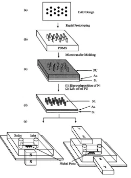
Deng et al. [31] reported a magnetic filtration system (figure 1.5), using arrays of
microfabricated nickel posts along with external field to generate high magnetic field
gradients in a microfluidic channel to trap magnetic beads moving in the flow. The nickel
posts were fabricated by electrodeposition through a soft-lithography defined mold, with
a height of 7μm, a diameter of 15μm and 40μm in spacing. The beads are with diameters
around 4.5μm. The fabricated Ni posts were then integrated into a PDMS microfluidic
channel 50μm tall and 150μm wide, and placed into an external field of 500Gauss
generated by nearby rare earth permanent magnets, to form the microfiltration system.
According to the lumped/distributed magnetic system definition outlined in Table 1.1, the
application of this system is the magnetic beads, with the characteristic length of 4.5μm
11
40μm, defined by the spacing of Ni posts. Hence, this is a distributed magnetic system.
The utilization of the system is tested by flowing a solution containing 104 beads per milliliter with a flow rate of 2μL/h, controlled by micromanipulators. The system showed
a good bead-capturing capability, with a maximum of 50 beads trapped per post.
Figure 1.5 Schematics of the fabrication sequence of a magnetic filtration system using arrays of microfabricated nickel posts along with external field to generate high magnetic field gradients in
12
Ko et al. [29] reported a magnetic sorting system (figure 1.6), utilizing the high magnetic
gradient near the edge of the numerous micropores (traps) patterned on a NiFe film to
trap magnetically labeled target cells with a high throughput (>100mL/h) for
immunomagnet sorting applications. In order to achieve a 100X greater throughput, the
authors converted the conventional lateral flow inside of a microfluidic channel that
subjected to clogging into a vertical flow through numerous through-film pores on a NiFe
film. Through-film circular pores 30μm in diameter and 30μm apart on 12μm thick NiFe
films, for example, have been achieved by electroplating through a reusable polyimide
master mold, followed by a mechanical peel-off of the plated films from the Cu substrate,
without destroying micro-sized features in the master mold, as a way for cost reduction.
A film bearing pores was then incorporated into the sorting system using a polyester film
packaging and a fluid reservoir. A blunt syringe tip was connected to the system to pull
the fluid out from the reservoir. According to the lumped/distributed magnetic system
definition outlined in Table 1.1, in this system, the magnetic-nanoparticle-labeled target
cells as an application with a 20μm characteristic size (cell diameter plus nanometer sized
magnetic nanoparticles) is less than the spatial wavelength of the system (30μm), defined
by the lateral spacing between the micropores. Hence the fabricated NiFe film bearing
traps is a distributed system. By largely improving throughput from 5mL/hr to 100mL/hr
along with the economically scalable fabrication approach, this design of magnetic
sorting system would help to meet the need of processing of large volumes of clinical
13
Figure 1.6 A magnetic sorting system (MagNET) [29] utilizing the high magnetic gradient near the edge of the numerous micropores (traps) patterned on NiFe films to trap magnetically labeled
target cells with high throughput (>100mL/h) for immunomagnet sorting. (a) MagNET isolate cells targeted with functionalized magnetic nanoparticles; MagNET rotates the conventional microfluidic geometry (b) by 90° to form magnetic traps for vertical flow(c); (d) Micrographs of Track Etched Magnetic microPOre (TEMPO) devices; (e) Micrographs of MagNET devices and (f) a graph Summarizing relationship between % open area and % overlap for both TEMPO and
MagNET devices.
14
Figure 1.7 Concept of rotationary synchronous micromotors [32].
Benefiting from large output torque, high efficiency and long operation lifetime,
electromagnetic micromotors are suitable micro-actuators for various MEMS
applications, for example, as pumps for microfluidic applications, and as propellers for
micro-robots [33, 34]. The most common type of such permanent magnet micromotors is
a three-phase, axial-flux rotational synchronous micromotor, as one example
demonstrated by Feldmann et al. [32], shown in figure 1.7. The two most important
components in such devices are the rotor, comprised of multipoled permanent magnets
generating magnetic field parallel to the axis of the rotation (hence the axial flux); and the
stator windings with microfabricated copper coils on silicon or ferrite substrates [33, 35].
The alternating magnetic poles can be realized either by assembling of discrete magnets
or by impressing pole patterns into a contiguous magnet [35]. The arrangement of the
coils and magnets allows the motor driving by three phases. Namely, the three-phase
supply produces a rotating magnetic field in the stator windings, in turn generating a
torque on the multipoled permanent magnets, exciting the rotor revolving near the
15
stator and rotor poles, the characteristic length of the application (twice of the pitch of the
stator winding poles) is equal to the spatial wavelength of the system (twice of the pitch
of the rotor poles). According to the lumped/distributed magnetic system definition
outlined in Table 1.1, the multipoled permanent magnets shown above is a distributed
system.
1.4 Research objective and dissertation structure
The objective of this thesis is three-fold: 1) to develop a technology capable to
controllably and conveniently scale the relative dimensions of the characteristic length of
an application and the spatial wavelength of a device in a CMOS-compatible and fully
integrated manner, for both lumped and distributed systems; 2) to design, build and test
the systems using the developed technologies demonstrating the flexibility and versatility
of the technology.
The structure of this dissertation is shown in Figure 1.8. The present chapter reviewed the
lumped and distributed magnetic MEMS systems, paving the way for a fabrication
technology capable of controllably and conveniently scaling the relative dimensions of
the competing length scales (LC and λ) that defines the lumped/distributed systems in such a way that both types of systems could be design and fabricated facilely and flexibly
at the designer's will. Chapter 2 will detail the proposed fabrication technology:
through-mold robotic-assisted multilayer electrodeposition technology (Microlamination
Technology in short). First, the concept of robotic-assisted multilayer electrodeposition
16
electrodeposition system. Second, fabrication procedures of several conventional thick
photoresist molds and a high-aspect-ratio (HAR) UV-LIGA mold will be discussed,
intended to be used in conjunction with the robotic-assisted multilayer electrodeposition
technology for the paradigms of lumped and distributed magnetic systems enabled by the
fabrication technology. Chapter 3 will elaborate on a paradigmatic lumped magnetic
system based on the Microlamination Technology: microlaminated permanent magnets
with preserved magnetic properties. Chapter 4 will discuss the design, fabrication, and
characterization of a paradigmatic distributed magnetic system based on the
Microlamination Technology: a bi-stable vertical magnetic actuator with non-contact
latching behavior. Chapter 5 will conclude this dissertation and present possible future
works.
Figure 1.8 Dissertation outline.
Ch 1. Introduction
Ch 2. Fabrication Technology:
Through-mold sequential multilayer electrodeposition technology
HAR UV-LIGA mold for dual-heightstructures Conventional thick mold
for uniform-heightstructures
Ch 4. Distributed System
Bi-stable vertical magnetic actuator
Ch 3. Lumped System
17
CHAPTER 2FABRICATION TECHNOLOGY 2.1 Technology Overview
Through-mold robotic-assisted multilayer electrodeposition technology (Microlamination
Technology in short) discussed in this chapter is capable of creating two-and-a-half
dimensional (2.5D) uniform- or dual- height volumetric MEMS multilayer structures
with precisely controlled individual layer thicknesses at the smaller scale (tens of
nanometers to a few micrometers) and monolithic metallic structures (tens to hundreds of
micrometers in thickness) at the larger scale. The smaller scale fine structures are an
essential enabler for distributed systems while the larger volumetric structures provides
the desirable extrinsic properties (e.g. sufficient force or sensitivity, which are normally
volume-dependent) that are typically desirable [36-40] for MEMS applications.
In this chapter, we will break down the Microlamination Technology into modular
processes comprised of one chief technology: robotic-assisted multilayer
electrodeposition technology, and one auxiliary technology: thick plating-mold
fabrication technology capable of building two types of molds of interest: 1) a
conventional thick resist mold for uniform-height structures, and 2) a high-aspect-ratio
(HAR) UV-LIGA mold using which dual-height MEMS metallic structures separated by
narrow gaps can be realized. For demonstration purposes, when applicable, the processes
of the thick plating-mold fabrication technology in the present chapter will be illustrated
in combination with single-layer nickel electrodeposition. The actual incorporation of
18
2.2 Robotic-assisted Multilayer Electrodeposition Technology
Through-mold robotic-assisted multilayer electrodeposition is conceptually
straightforward. Electrodeposition of each individual layer of the multilayer structure
occurs in its individual electroplating bath (a solution that normally contains metal salts,
supporting ions, and stress-reduction agents), where sample is connected to the negative
terminal of the power supply and a sacrificial (dissolvable) or non-sacrificial anode is
connected to the positive terminal of the power supply (figure 2.1(a)). Upon immersing a
sample into a bath, a closed circuit forms through the electrolyte and film growth initiates
(metal ions in the electrolyte are reduced at the interface between the solution and the
sample surface). The electrodeposition of one layer of material could be followed by the
electrodeposition of another layer of materials, and further continues. Through this
sequential and repetitive layer-by-layer deposition, volumetric structures (normally tens
to hundreds of micron thick) comprised of thin individual layer (down to tens of
nanometers) could be fabricated. The introduction of automatic tools such as a robotic
arm greatly enhances the precision and consistency throughout the process and at the
same time reduces the labor of handling. Since each layer has its dedicated bath,
theoretically no restrictions exist for the number of materials involved or the sequence of
the comprising layers. For demonstration purposes, two bathes corresponding to material
A and B are shown in figure 2.1(a). Two power supplies are used to provide desired
current densities for each material deposition, with both of their positive terminals
connecting to the individual anodes, while negative terminals connecting to the sample.
19
for material A, until the desired individual thickness achieved. After which, the robotic
arm pulls the wafer out of the bath A and rinse in deionized water (DI water) to avoid
cross-contamination before placing into the bath B for the B material electrodeposition.
After rinsing in DI water, the robotic arm carries the wafer again into bath A for another
layer of material A, so on and so forth.
Figure 2.1 (a) schematic of the robotic-assisted multilayer electrodeposition system setup with exemplary two bathes and a rinsing DI water tank; (b) cross-sectional schematic showing a die of
a through-mold deposited multilayer structure with A/B/A/B/A/B layers (three pairs of A/B multilayers), the first layer deposition of A occurs on top of a conductive seed layer, the rest of
the layers deposited on top of the respective underlying layers.
A schematic of an exemplary through-mold deposited multilayer structure with
A/B/A/B/A/B layers is shown in figure 2(b). The smallest repeating unit of a certain
sequence in a multilayer structure is called a pair, such as the example in figure 2(b), A/B
is one pair and a total of three pairs are shown. The first layer of electrodeposition occurs Substrate
(b)
Mold Material B
Material A Seed layer
Bath A
Power Supply 1
Power
Supply 2 Bath B Rinse
(DI)
anode A anode B
sample
(a)
20
within an insulating mold on top of a conducting substrate (seed layer) that is connected
to the negative terminal of the power supply. The following rounds of electrodeposition
occur inside the mold (as long as the mold is sufficiently tall) on top of the underlying
layers (as long as the underlying layers remains conductive after being deposited), using
the layers underneath as an effective substrate. The individual layer thickness is
controlled by both current density and plating time, as governed by the Faraday’s law of
electrolysis shown in equation (1), where h is the thickness (in meters) of the deposited
metal, η is the current efficiency (normally not 100%, due to parasitic reactions, e.g.
hydrogen evolution at the cathode), I is the current input (in Ampere), A is the platable
area (in meter squared, defined by mold), M molar mass of the substance (in gram per
mole), t is the plating time (in second), z is the valency number of ions of the plated
material (unitless), F is Faraday's constant (96485 Coulomb per mole) , ρ is the density of
the plated material (in gram per meter cubed). Due to the fact that current efficiency
might not always be 100%, the calculated target thickness of the deposits (h) using
equation (2.1) might not be precise. It is recommended that a dummy sample should be
used to experimentally verify the thickness of deposits. A common method is to assume a
100% current efficiency to calculate the plating time to start with, and account for any
discrepancy of theoretical and experimental thickness differences into current efficiency
21
Figure 2.2 In-house built robotic-assisted electrodeposition system. (a) Zoomed-out view, system comprised of robotic arm, machine guard, power supply, bath tray, microcontroller and controlling software. (b) Zoomed-in view for bath tray, showing two bathes, 2 rinsing DI water
containers, and a sample holder.
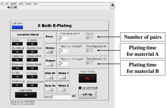
Figure 2.3 In-house programmed LabVIEW graphical user interface (GUI). The end user can vary the number of pairs and plating time for both materials. While running, the interface will indicate location of the wafer, the current layer status in the sequence, as well as the elapsed
plating time in each bath to the user. LabVIEW
Controlling Interface
Machine Guard
Robotic Arm
Power Supply
Bath 1 Bath 2
Microcontroller
DI (2)
(a) (b)
Sample Holder
Bath Tray
Number of pairs
Plating time for material A
22
An in-house built robotic-assisted electrodeposition system (referred to as the robot from
now on) has been assembled (figure 2.2), converted from a commercially available CNC
mill (PRO4824, CNCRouterParts). The robot is composed of six components shown in
figure 2.2(a): (1) a robotic arm capable of moving in three axes; (2) a bath tray for
multiple bathes and rinsing containers (DI water) as indicated in figure 2.2(b); (3) a
programmable DC power supply (Keithley2220 dual-channel); (4) an in-house designed
machine guard (McMasterCarr); (5) a microcontroller (Nema34, CNCRouterParts) and
(6) a controlling PC with in-house programmed LabVIEW controlling interface. We
choose to program the robot using LabVIEW due to friendly graphical user interface
(GUI) LabVIEW offers for the end users in our lab, as well as to facilitate the potential
integration of other LabVIEW-ready instruments into the electrodeposition system. The
LabVIEW GUI for the robot is shown in figure 2.3. Three parameters need to be input by
users: number of pairs, plating time for both materials A and B. These parameters along
with input current densities and other plating parameters will define the microlamination
structures to be fabricated.
23
Figure 2.4 Fabrication sequence (side view) of conventional thick resist mold for uniform-height structures. (a) Sputtering of Ti/Cu/Ti seed layer on substrate (e.g. Si or glass); (b) spinning and patterning of the thick resist mold; (c) exposed top Ti seed layer wet-etched immediately before
electrodeposition; (d) electrodeposition of Ni layer; and (e) optional resist mold stripping. The final structures all have uniform height.
2.3 Thick Plating-mold Fabrication Technology
2.3.1 Conventional Thick Resist Mold for Uniform-height Structures
One of the common themes in the field of MEMS is the desire of microstructures with
relatively large volumes (or large thicknesses with a given footprint, normally a few to a
few hundred micrometers). The fundamental reason for this desire is that most likely, the
sensitivity of a MEMS sensor or the collectable forces of a MEMS actuator relates to
volume-dependent properties. For example, in an electrostatic MEMS stepper motor, the
electrostatic force is directly proportional to the height of the micromachined electrodes
[41]; in a magnetic energy harvester, it is the magnetic flux rather than the flux density is
of importance [25]; in a micromachined compass, it is the volumetric magnetization
Ni Thick resist
Cu
(a) (b)
Substra te Ti
(c) (d)
24
rather than magnetization itself is of relevance [9]. It is hence critical to develop suitable
technologies for volumetric microstructure fabrication.
The traditional bulk-micromachining techniques to fabricate thick microstructures (and
related high-aspect-ratio microstructures) include LIGA (German acronym for
lithography, electroplating and moulding) and DRIE (silicon deep reactive ion etching)
[42]. Thick mold fabrication is a prerequisite of the electrodeposition, and hence are of
critical importance to LIGA structures. Conventional thick resist molds for fabricating
uniform-height structures via electrodeposition will be discussed in this section. Various
thick photoresists could be used to prepare the mold for this process, including
chemically-inert resists and removable resists, the details of which are discussed below.
The fabrication sequence (side view) of uniform-height structures via through-mold
electrodeposition is shown in figure 2.4. A substrate (e.g. silicon or glass) was cleaned
using Piranha Solution (3:1 volume ratio of sulfuric acid and hydrogen peroxide)
followed by an hour-long dehydration bake in a convection oven at 110C. A seed layer
comprising copper (300nm) sandwiched by titanium (30nm) layers was then formed
using DC sputtering (Denton Explorer14) shown in figure 2.4(a). The top titanium layer
serves the purpose of 1) reducing possible oxidation of the copper seed layer on which
the plated metallic structures grow; and 2) enhancing the adhesion of the photoresist
mold to the seed layer. The bottom titanium layer enhances the adhesion of the structures
to the substrate. The substrate with Ti/Cu/Ti seed layer was then cleaned with solvent
25
create thick molds for electrodeposition (figure 2.4(b)) depending on the applications of
the fabricated structures and devices.
2.3.1.1 Chemically-inert Resist
SU8 is an epoxy based chemically amplified negative resist. SU8 has two prominent
properties [43]: 1) high optical transmittance beyond the wavelength of 360nm; 2)
superior thermal and chemical resistance. The former property makes it ideal for thick,
HAR photoresist structures with straight wall-profiles, the latter property has enabled
permanent structures made by SU8 such as microfluidic channels [44] and microgears
[45]. Here a procedure for a 160μm-thick SU8-2050 mold is documented.
The resist was dispensed over the wafer manually. A two-step spinning was implemented
to achieve a 160μm thickness with a pre-spin of 500rpm/10s and a main-spin of
1000rpm/30s. After edge bead removal, the substrate was left to sit on a leveled surface
for 3 minutes to aid the planarization of the resist. The wafer was then soft-baked on a
contact hotplate (65C/7min + 95C/30min), after which the hotplate was turned off till
the wafer reaching the room temperature (normally takes more than a few hours). The
wafer was then exposed with a 364mJ (i-line) dose in the vacuum contact mode through
both a chrome mask and a 360nm long-pass filter. The application of the long-pass filter
helps to obtain vertical sidewall profile as the wavelength below 360nm shows a low
transmittance [43]. A temperature ramping post-exposure bake (from room temperature
to 95C at a ramping rate of 180C/h + 95C/120min + from 95C to room temperature at
26
shock to the thick SU8 structures that might cause delamination. The wafer was then
developed upside down in SU8 developer (MicroChem) followed by an isopropyl alcohol
rinse. An absolutely clean SU8 resist stripping without any residue left behind is
extremely hard and might be incompatible with the deposited metallic structures, that
said, a few methods exist which were reviewed somewhere else [46].
2.3.1.2 Removable Resists
Table 2.1 Mold heights and stripping methods for various removable resist.
Removable resists are desired especially when post-processing is needed that can only be
carried out after stripping the resist molds. Both the cleanness of the resist removal and
process simplicity (i.e. in some cases, wet removal using solvent is preferable over
plasma etching due to process compatibility) are essential for these applications. Here we
will discuss five removable resists (SPR220-7 (6.5μm), AZ4620 (12μm), AZ40XT-11D
(20μm), NR26-25000P (50μm), and KMPR1050 (100μm))) for molds of different heights
Resist Documented height
Maximum height w/ single spin
Stripping method Easiness of fabrication Resist wall profile SPR220-7 6.5μm/ 4000rpm 12μm/ 1000rpm Acetone/ O2plasma
Easy Slanted AZ4620 12μm/ 1500rpm 17μm/ 1000rpm Acetone/
O2plasma Easy Slanted
AZ40XT-11D 20μm/ 3000rpm
65μm/ 720rpm
Acetone/ O2plasma
Hard Near-vertical NR26-25000P 50μm/ 1500rpm 100μm/ 1000rpm Acetone/ O2plasma
Medium Slanted KMPR1050 100μm/ 1000rpm 100μm/ 1000rpm NMP/ O2plasma
27
ranging over 7-100μm. These resists were selected due to three reasons: 1) their
availability at Georgia Tech’ and Penn’s nanofabrication facilities; 2) to cover a wide
range of mold thicknesses (a few to a hundred micrometer) for different applications; and
3) fabrication simplicity (e.g. SPR220-7 and AZ4620, no stepping/ramping bake or
post-exposure bake) or vertical resist wall profiles (e.g. AZ40XT-11D and KMPR1050,
important for actuator applications detailed in the Chapter 4). Their documented height
(with the fabrication procedure in the present section), maximum height by a single spin
(from resist manuals), resist stripping methods, easiness of fabrication, and qualitative
sidewall profiles are summarized in Table 2.1.
SPR220-7 is a positive photoresist capable of achieving thicknesses ranging from
5.5-12μm [47]. The detailed process of a 6.5μm-thick plating mold is as follows. The resist
was manually dispensed onto the substrate bearing the seed layer. A two-step spinning
procedure with a pre-spin of 500rpm/10s and a main-spin of 4000rpm/30s was used. A
soft bake of 110C/180s on a contact hotplate was implemented. After soft baking, the
resist was cooled down for 10 minutes to room temperature. The wafer was then exposed
with a dose of 380mJ (i-line) using a UV mask aligner (Karl Suss MA6) through a
chrome mask in the vacuum contact mode. A post-exposure bake of 105C/60s was
carried out on a contact hotplate, after which the wafer was removed and let to cool down
to room temperature. The exposed wafer was then developed in a dedicated resist
developer MF26A (MicroChem) for 105s at room temperature.
AZ4620 is a positive photoresist capable of achieving thicknesses ranging from 6-17μm
28
manually dispensed onto the substrate bearing the seed layer. A two-step spinning
procedure with a pre-spin of 500rpm/10s and a main-spin of 2000rpm/30s was used. A
soft bake of 90C/180s on a contact hotplate was implemented. After soft baking, the
resist was cooled down for 10 minutes to room temperature. The wafer was then exposed
with a dose of 1000mJ (i-line) using a UV mask aligner (Karl Suss MA6) through a
chrome mask in the vacuum contact mode. The exposed wafer was then developed in a
DI water diluted resist developer AZ400K (25% vol.) for 130s at room temperature.
Thick positive photoresist AZ 40XT-11D (MicroChemicals) has been shown to have
nearly vertical resist wall profiles [49, 50]. The detailed process of a 20μm-thick plating
mold is as follows. The resist was manually dispensed onto the substrate bearing the seed
layer. To achieve a 20μm thickness, a two-step spinning procedure with a pre-spin of
500rpm/10s and a main-spin of 3000rpm/30s was used. In order to prevent the formation
of bubbles in the resist film during the soft bake, a temperature-stepping soft bake
(65C/60s + 95C/60s + 125C/300s + 95C/60s + 65C/60s) on a contact hotplate was
implemented. After soft baking, the resist was cooled down for 10 minutes to room
temperature. The wafer was then exposed with a dose of 300mJ (i-line) using a UV mask
aligner (Karl Suss MA6) through a chrome mask in the vacuum contact mode. A
post-exposure bake of 105C/60s was carried out on a contact hotplate and let to cool down to
room temperature. The exposed wafer was then developed in a dedicated resist developer
AZ 726MIF (MicroChemicals) for 210-240s at room temperature.
NR26-25000P is a negative photoresist capable of achieving thicknesses ranging from
29
resist was manually dispensed onto the substrate bearing the seed layer. A two-step
spinning procedure with a pre-spin of 500rpm/10s and a main-spin of 1500rpm/30s was
used. A temperature-stepping soft bake (80C/240s + 150C/210s) on a contact hotplate
was implemented. After soft baking, the resist was cooled down for 10 minutes to room
temperature. The wafer was then exposed with a dose of 800mJ (i-line) using a UV mask
aligner (Karl Suss MA6) through a chrome mask in the vacuum contact mode. A
post-exposure bake of 90C/300s was carried out on a contact hotplate and let to cool down to
the room temperature. The exposed wafer was then developed in a dedicated developer
RD6 (Futurrex).
KMPR1050 is a chemically amplified thick negative photoresist with HAR capability and
straight wall-profile, has been reported as an SU8 alternative for UV LIGA process with
improved removability [52, 53]. The detailed process of a 100μm-thick plating mold is as
follows. A two-step spinning was implemented to achieve 100μm thickness with a
pre-spin of 500rpm/10s and a main-pre-spin of 1500rpm/30s. After edge bead removal, the wafer
was left to sit on a leveled surface for 3 minutes to aid the planarization of the resist. The
wafer was then soft-baked on a contact hotplate at 100C/30min. After cooling down to
room temperature, the wafer was exposed with a 1300mJ (i-line) dose in the vacuum
contact mode through both a chrome mask and a 360nm long-pass filter. The application
of the long-pass filter helps to obtain vertical sidewall profile as the wavelength below
360nm shows a low transmittance similar to SU8 [52]. A temperature stepped
post-exposure bake (65C/120s + 95C/240s + 65C/120s) was carried out on a contact
30
down in SU8 developer (MicroChem) for 7 minutes followed by an isopropyl alcohol
rinse.
After resist mold fabrication, prior to electrodeposition, an O2 descum process was carried out to remove any possible photoresist residue. The exposed top titanium layer in
the Ti/Cu/Ti seed layer stack was wet etched (figure 2.4(c)) in a diluted hydrofluoric acid
solution (0.25% vol.) immediately before commencement of electrodeposition. For
demonstration purposes, conventional single-layer through-mold electrodeposition of
nickel (figure 2.4(d)) was implemented using a DC current source with current density of
10mA/cm2 in a nickel electrodeposition bath [54] consisting of 200g/L NiSO4·7H2O, 5g/L NiCl2·6H2O, 25g/L H3BO3, and 3g/L saccharin, with a pH of 2.5-2.8. The plating rate was measured to be 6.5μm per hour. Plating occurred at room temperature with no
agitation. Whenever needed the single-layer electrodeposition could be conveniently
replaced by robotic-assisted multilayer electrodeposition using the automated multilayer
electrodeposition system. Lastly, optional resist mold stripping can be further carried out
and the uniform-height metallic structures (figure 2.4(e)) are readily fabricated.
2.3.2 HAR UV-LIGA Mold for Dual-height Structures Separated by Narrow Gaps
Vertical actuators with large stroke have been shown to play an important role in optical
and electrical applications [55, 56]. Various transduction mechanisms have been
proposed to realize vertical actuation, among which, electrostatic [55] and magnetic
actuators [57] most of which rely on vertically displaced electrodes (comb fingers) or
31
that they are initially vertically misaligned, and as actuation occurs, they are snapped into
alignment at the same vertical height level. Moreover, it is often optimal for the
electrodes/magnetic poles to be separated by narrow gaps in order to enhance the
actuation force [55]. This height difference in poles, together with the narrow gaps that
separate them, normally necessitates multiple masks [55, 56]. In this section, we will
describe a process that addresses this challenge using a single mask to create
fully-isolated, dual-height MEMS metallic structures separated by narrow gaps on a
transparent substrate.
The technology described here is capable of achieving dual-height MEMS metallic
structures separated by narrow-gaps as long as four (4) design considerations are met (see
figure 2.5(a) for illustration): 1) the thinner structure (A) and the thicker structure (B) in
the dual-height structures are fully isolated by a continuous gap (G); 2) the thinner
structure resides inside of the gap forming an island whereas the thicker structure resides
on the periphery; 3) the thicker structure always has identical materials with the thinner at
the same vertical height level; and 4) a transparent substrate is needed for the dual-height
structures to be built on. The proposed fabrication sequence is a modified conventional
through-mold electrodeposition: the gap area will be occupied by photoresist molds twice
(figure 2.5(b)), whereas the remaining areas will be electroplated twice, forming the
32
Figure 2.5 (a) 3-D schematic of the exemplary dual-height structures after fabrication. Inner island A is the thinner structure, enclosed by a continuous white area G, the gap. On the periphery
is the thicker structure. (b) Schematic of the structures during fabrication. The photoresist mold used for the through-mold electrodeposition is shown. The mold will be removed after plating,
forming the continuous gap G of figure 2.1(a) between the dual-height structures.
The process relies on two self-aligned steps enabled by the electrodeposited thinner
structures: a wet-etching of the seed layer utilizing the thinner structure as an etch-mask
to electrically isolate the thinner and thicker structures, and a backside UV lithography
utilizing the thinner structure as a lithographic mask to create a high-aspect-ratio mold for
the thicker structure through-mold electrodeposition.
A schematic of the fabrication is shown in figure 2.6. A soda lime glass slide (Corning)
was cleaned using Piranha Solution followed by an hour-long dehydration bake in a
convection oven at 110C. A seed layer comprising copper (300 nm) sandwiched by
titanium (30 nm) layers was then formed using DC sputtering (Denton Explorer14).
A (thinner) B
(thicker)
G X
X’
(b) (a)
33
Figure 2.6 Fabrication sequence (side view, cross-section X-X’ of Figure 2.5). (a) Sputtering of Ti/Cu/Ti seed layer on glass substrate and patterning positive resist mold; (b) top Ti seed layer
wet-etched and electrodeposition of Ni layer; (c) positive resist mold stripping followed by exposed seed layer wet-etching, electrically insulating the inner (thinner) structure; (d) negative resist spinning and backside UV exposure; (e) negative resist development, forming a self-aligned mold; (f) electrodeposition of Ni on the outer (thicker) structure only; and (g) negative resist mold
stripping.
The glass substrate with Ti/Cu/Ti seed layer was then cleaned with solvent, followed by
an O2 descum (Technics RIE, 110sccm O2, 100W, 30s). This first lithography step was intended to create a photoresist mold for the first plated metallic layer that will
functionally serve as a mask-equivalent for subsequent wet-etching and lithography steps,
as well as structurally realize the entirety of the thickness of the thinner structure, and
partially realize the thickness of the thicker structure. Both positive and negative
photoresists are suitable for this lithography step, but one caveat is that due to the
mask-equivalent nature of this layer, pattern non-idealities will propagate throughout Ni KMPR AZ 40XT
Cu UV
(a) (b)
(d)
Gla ss Ti (c)
insulated
UV
(e) (f)
(g)
34
subsequent process steps. Hence, in general, a straighter wall-profiled photoresist with a
thickness larger than that of the desired first plated metallic layer is preferable for this
step. For demonstration purposes, a chemically amplified thick positive photoresist AZ
40XT-11D (MicroChemicals) with nearly vertical resist wall profile [49, 50] was used for
the first lithography step to create a 20μm plating mold. The detailed process for pattering
this photoresist is can be found in section 2.3. This concludes the first lithography process
as shown in figure 2.6(a).
Prior to electrodeposition, an O2 descum process was carried out to remove any possible photoresist residue. The exposed top titanium layer in the Ti/Cu/Ti seed layer stack was
wet etched in a diluted hydrofluoric acid solution (0.25% vol.) immediately before
commencement of electrodeposition. Conventional through-mold electrodeposition
(figure 2.6(b)) was implemented using a DC current source with current density of
10mA/cm2 in a nickel electrodeposition bath [54]. The plating rate was measured to be 6.5μm per hour. Plating occurred at room temperature with no agitation. The target
thickness of this layer plating is the thickness of the thinner structure in the dual-height
structures. After electrodeposition, the plating mold was subsequently stripped in
acetone.
Using the previously plated nickel layer as a wet-etching mask, the copper conductive
layer and bottom titanium adhesion layer in the Ti/Cu/Ti seed layer stack originally
underneath the resist mold were selectively wet etched using diluted hydrofluoric acid
(0.25% vol.) and a saturated solution of copper sulfate in ammonium hydroxide [58],
![Figure 1.1(a) a collection of refrigerator magnets [15] as a demonstration of lumped magnetic systems](https://thumb-us.123doks.com/thumbv2/123dok_us/9234550.1459040/22.612.151.491.339.574/figure-collection-refrigerator-magnets-demonstration-lumped-magnetic-systems.webp)
![Figure 1.6 A magnetic sorting system (MagNET) [29] utilizing the high magnetic gradient near the edge of the numerous micropores (traps) patterned on NiFe films to trap magnetically labeled](https://thumb-us.123doks.com/thumbv2/123dok_us/9234550.1459040/31.612.163.488.67.356/magnetic-utilizing-magnetic-gradient-numerous-micropores-patterned-magnetically.webp)
![Figure 1.7 Concept of rotationary synchronous micromotors [32].](https://thumb-us.123doks.com/thumbv2/123dok_us/9234550.1459040/32.612.221.408.81.226/figure-concept-rotationary-synchronous-micromotors.webp)