Structure Generation and Design of Multiple Loop
Feedback OTA-Grounded
Capacitor Filters
Yichuang Sun,
Member, IEEE, and J. Kel Fidler
Abstract—This paper addresses the structure generation,
anal-ysis and synthesis of multiple loop feedback OTA-C filters. A systematic approach is proposed for all-pole filters, and the generation and design of minimum component structures are extensively exemplified. Two general methods for transmission zero realization are also suggested and two architectures with sim-ple design formulas are illustrated. Using the theory many new interesting configurations can be produced alongside some known structures. All the filter architectures contain only grounded capacitors and all internal nodes in canonical realizations have a grounded capacitor. A general method for sensitivity analysis of the structures is formulated. Numerical design examples and simulation results are also presented. The essence of the theory is the establishment of the relationship between the filter structure and the feedback matrix, which makes systematic structure generation and general design equation formulation possible.
Index Terms—Active filters, analog circuit design, analog signal
processing, continuous-time filters, OTA-C filters.
I. INTRODUCTION
A
CTIVE FILTER DESIGN has been thoroughly investi-gated for operational voltage amplifier based active-filters. Three well-known methods, that is, the cascade of biquadratic sections, simulation based on passive ladder prototypes, and the multiple loop feedback have been very well established [1]. However, it has been found that op amp based active- filters are not suitable for high frequency operation, fully integrated implementation, and electronic tuning, and frequently are based on complex structures.Tremendous efforts have therefore been made over recent years to develop new alternative techniques in high frequency continuous-time filters. The OTA-C approach, in particular, uses the operational transconductance amplifer to displace the conventional operational voltage amplifer and associated resistors in active- filters and has achieved outstanding performance improvement in structural simplicity, electronic tunability, high frequency capability, and monolithic integra-bility. This technique has hence received most attention [2] and has become today the main approach for high-frequency full-integration filtering.
Manuscript received June 6, 1995; revised January 14, 1996. This paper was recommended by Associate Editor D. Haigh.
Y. Sun is with the Department of Electrical and Electronic Engineering, University of Hertfordshire, Hatfield Herts AL 10 9AB, U.K.
J. K. Fidler is with the Department of Electronics, University of York, York Y01 5DD, U.K.
Publisher Item Identifier S 1057-7122(97)00813-1.
At present the performance of low-order OTA-C filters has been proved and a body of literature has been published for the design of second-order OTA-C filters [3]–[8]. Research has turned to the realization of high-order specifications [8]–[21]. For high-order OTA-C filter synthesis, cascade design based on biquadratic sections has been most widely used. Research has been directed to simulation techniques [9]–[11] as well. Some researchers have also explored the feedback coupled-biquad method [12], [13], although this well-known filter design method has not received equal attention, compared with the other two. No matter what the approach, the filter structures almost always consist of integrators and amplifiers as the most basic building blocks, and have feedback loops in this basic level. A general approach may be therefore developed based on the multiple loop feedback structure constructed with integrators and amplifiers.
Practical considerations in high frequency OTA-C filter design may specify using grounded capacitors and reduc-ing the number of components. The former is because the grounded capacitor can be implemented on a smaller area than the floating counterpart and it can absorb equivalent shunt capacitive parasitics. The latter is due to the fact that a large number of components may increase power con-sumption, chip areas, noise, and parasitic effects. Thus the design method and resulting filter structures should be based on grounded capacitors and canonical architectures, although noncanonical realizations may be required in some situations to achieve design flexibility or to satisfy some special spec-ifications.
This paper will show how to generate, analyze and de-sign multiple integrator loop feedback filter structures using OTA’s and grounded capacitors for synthesis of both trans-mission poles and zeros. General theory with a systematic scheme for generating all-pole filter structures is established in Section II, with concentration on minimum component OTA-C realizations in Section III, where the exhaustive enumera-tion of canonical filter structures is investigated. Secenumera-tion IV introduces two general methods for generation of transmis-sion zeros, together with illustrative examples. In Section V general sensitivity relations are established and Section IV presents some design and simulation examples. The paper concludes with a brief summary and some further com-ments.
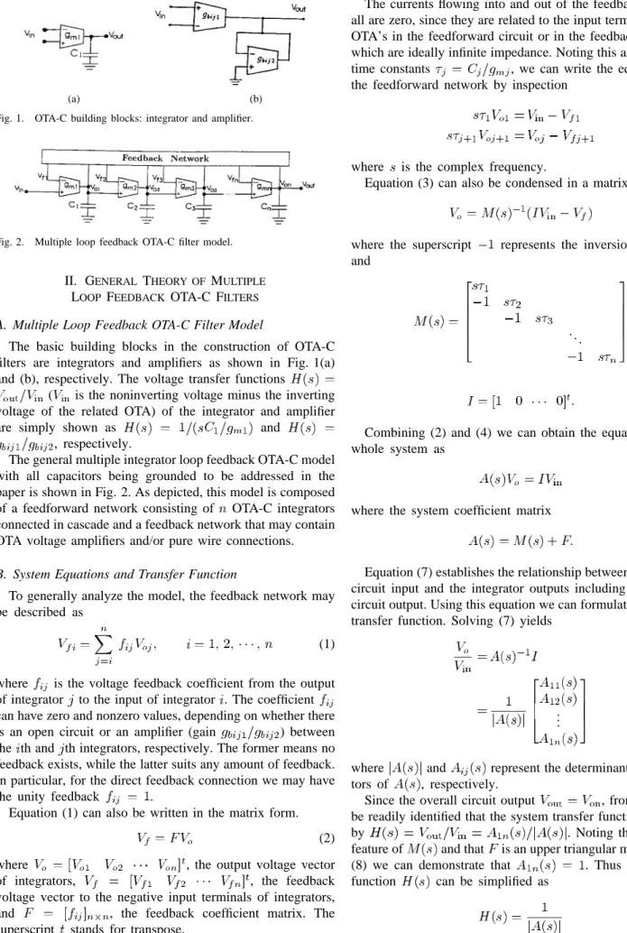
(a) (b) Fig. 1. OTA-C building blocks: integrator and amplifier.
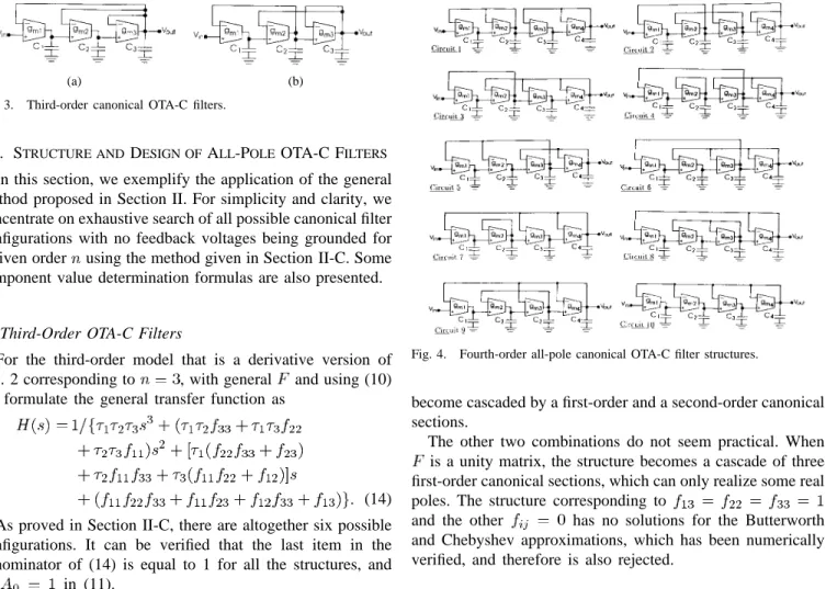
Fig. 2. Multiple loop feedback OTA-C filter model.
II. GENERAL THEORY OF MULTIPLE LOOP FEEDBACK OTA-C FILTERS A. Multiple Loop Feedback OTA-C Filter Model
The basic building blocks in the construction of OTA-C filters are integrators and amplifiers as shown in Fig. 1(a) and (b), respectively. The voltage transfer functions
( is the noninverting voltage minus the inverting voltage of the related OTA) of the integrator and amplifier
are simply shown as and
, respectively.
The general multiple integrator loop feedback OTA-C model with all capacitors being grounded to be addressed in the paper is shown in Fig. 2. As depicted, this model is composed of a feedforward network consisting of OTA-C integrators connected in cascade and a feedback network that may contain OTA voltage amplifiers and/or pure wire connections. B. System Equations and Transfer Function
To generally analyze the model, the feedback network may be described as
(1)
where is the voltage feedback coefficient from the output of integrator to the input of integrator . The coefficient can have zero and nonzero values, depending on whether there is an open circuit or an amplifier (gain ) between the th and th integrators, respectively. The former means no feedback exists, while the latter suits any amount of feedback. In particular, for the direct feedback connection we may have
the unity feedback .
Equation (1) can also be written in the matrix form. (2)
where , the output voltage vector
of integrators, , the feedback
voltage vector to the negative input terminals of integrators,
and , the feedback coefficient matrix. The
superscript stands for transpose.
The currents flowing into and out of the feedback network all are zero, since they are related to the input terminals of the OTA’s in the feedforward circuit or in the feedback network, which are ideally infinite impedance. Noting this and denoting
time constants , we can write the equations for
the feedforward network by inspection
(3) where is the complex frequency.
Equation (3) can also be condensed in a matrix form (4) where the superscript represents the inversion operation and
. .. (5)
(6) Combining (2) and (4) we can obtain the equation for the whole system as
(7) where the system coefficient matrix
(8) Equation (7) establishes the relationship between the overall circuit input and the integrator outputs including the overall circuit output. Using this equation we can formulate the circuit transfer function. Solving (7) yields
..
. (9)
where and represent the determinant and
cofac-tors of , respectively.
Since the overall circuit output , from (9) it can be readily identified that the system transfer function is given
by . Noting the structural
feature of and that is an upper triangular matrix, using
(8) we can demonstrate that . Thus the transfer
function can be simplified as
C. Feedback Coefficient Matrix and Systematic Generation of Filter Structures
The feedback matrix is defined by (2) and has the property that
if there is feedback between and otherwise
As can be seen from (2), if all the elements in a row of , say row , are zero, the corresponding feedback voltage will be zero and so is the converse. means that the inverting terminal of the OTA in the th integrator is grounded. Note that is an upper triangular matrix; for all nonzero
elements there are . If we further suppose that
no inverting integrator terminals are grounded, the feedback matrix will also have the property that each row has one and only one nonzero element, which implies that is always nonzero. The nonzero feedback coefficient can be realized using an OTA voltage amplifier and the unity feedback coefficient can also be achieved using pure wire connection, as an alternative to using a unity gain amplifier.
In the following by the canonical or minimum component realization we mean that for realizing the unity DC gain th-order all-pole low-pass filter, only OTA’s and capacitors (i.e., integrators) are required [14], [15]. For the general model in Fig. 2 the canonical realization is clearly equivalent to no components existing in the feedback network. Alterna-tively we can say that for canonical architectures, the feedback
matrix defined by (2) obviously has only zero
and unit elements, since feedback can only be achieved by direct connection.
It is apparent that there is an one-to-one correspondence between the feedback matrix and the circuit configuration and different will give rise to different circuit structures. To show this we consider the situation that feedback is realized only by direct connection and none of the OTA inverting terminals in the integrators are grounded. According to the features of the general discussed above, the feedback matrix now becomes an upper triangular (0, 1) matrix and has one and only one unit element in each row, leading to . Therefore for the th-order model there are combinations of unit element positions in the matrix. Note that the unit element in each combination is realized by a direct connection between the negative input terminal of integrator and the output of integrator . Thus we have different combinations of feedback connections, i.e., different filter structures.
It is of particular interest that this also suggests a method for generating all possible filter architectures that are canonical and without grounded integrator inverting terminals. That is, for any given order , we first find all combinations of unit element positions in . Direct connections are then made corresponding to all unit feedback coefficients in each combi-nation; this is repeated for all different combinations. This method is extensively studied and exemplified in Section III. D. Filter Synthesis Procedure Based on Coefficient Matching
From (5) and (8) we can see that the determinant may normally be an th-order polynomial of . The
trans-fer function in (10) may therefore have the all-pole filter characteristic.
The general form of all-pole low-pass transfer functions can be expressed as
(11) To synthesize this desired function we may follow the generic procedure shown below.
Based on (10), by expansion of we attain the circuit transfer function
(12) Comparing (11) and (12), to achieve the desired character-istic the following set of coefficient matching equations must be satisfied:
(13) Solving (13) we obtain and . To finish the design we
compute the values of each and from and .
The efficient expansion of to reach the polynomial form in of (12) is the first step in the design. Some symbolic analysis techniques may be required generally to deal with to get coefficient matching equations. However, the issue may be quite easily handled for low-order and some general high-order filters as will be shown in the next section. The coefficient match equations are usually nonlinear. Note that to produce the item , there is at least one group of integrators making a multiplicative contribution to the
corresponding coefficient. Hence will contain at
least one term of multiplication of integration constants . In most cases a nonlinear equation solver may be invoked to solve the derived parameter value determination equations. In Section III we will show that the design equations of many structures can also be easily solved explicitly.
To further determine each and there exist degrees of freedom in the canonical realization and more than degrees in the noncanonical. Thus the transconductances or the capacitances can be arbitrarily assigned to be identical. Taking the canonical realization as an example we may set
and then calculate ,
for any or let and then compute
.
As can be seen from (8) the network performance is a function of . Different will lead to different transfer characteristics in (10). is also linked with filter structures and different will correspond to different architectures. Thus the relationship between the performance and the structure is established through the feedback matrix. The significance is even more in that the generality and systematicality of the design method is obtained due to the introduction of .
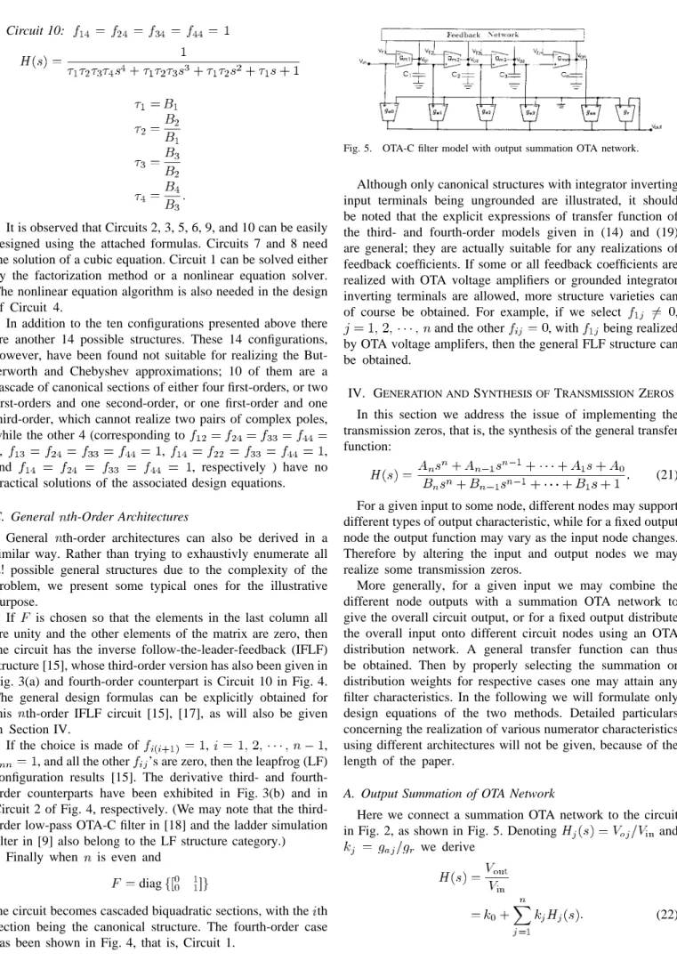
(a) (b) Fig. 3. Third-order canonical OTA-C filters.
III. STRUCTURE ANDDESIGN OFALL-POLEOTA-C FILTERS In this section, we exemplify the application of the general method proposed in Section II. For simplicity and clarity, we concentrate on exhaustive search of all possible canonical filter configurations with no feedback voltages being grounded for a given order using the method given in Section II-C. Some component value determination formulas are also presented.
A. Third-Order OTA-C Filters
For the third-order model that is a derivative version of Fig. 2 corresponding to , with general and using (10) we formulate the general transfer function as
(14) As proved in Section II-C, there are altogether six possible configurations. It can be verified that the last item in the denominator of (14) is equal to 1 for all the structures, and
so in (11).
When and the other elements are
zero, we have the structure in Fig. 3(a) and the circuit transfer function in (14) becomes
(15) The parameter value equations are demonstrated as
(16)
If we select and the other , the
filter architecture in Fig. 3(b) results. The corresponding trans-fer function and the parameter value determination formulas are derived as
(17)
(18)
For with and the other ,
or and the other , the circuits
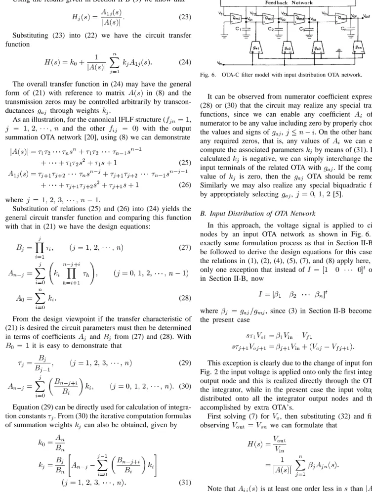
Fig. 4. Fourth-order all-pole canonical OTA-C filter structures.
become cascaded by a first-order and a second-order canonical sections.
The other two combinations do not seem practical. When is a unity matrix, the structure becomes a cascade of three first-order canonical sections, which can only realize some real poles. The structure corresponding to
and the other has no solutions for the Butterworth and Chebyshev approximations, which has been numerically verified, and therefore is also rejected.
B. Fourth-Order OTA-C Filters
For the fourth-order general model of Fig. 2, again from (8) and (10) the general transfer function can be written with some tedious manipulation as
(19) For any particular we can easily draw the associated struc-ture, obtain the corresponding transfer function, and calculate the component values. There are altogether 24 combinations of possible filter configurations according to the discussion in Section II-C. Ten practical structures are shown in Fig. 4 and the corresponding ’s, transfer functions, and some design formulas are presented below. Note that in each case the ’s that are not written out are treated as zero and the realization of the unity dc gain all-pole characteristic in (11) with is dealt with.
Circuit 1: Circuit 2: (20) Circuit 3: Circuit 4: Circuit 5: Circuit 6: Circuit 7: Circuit 8: Circuit 9:
Circuit 10:
It is observed that Circuits 2, 3, 5, 6, 9, and 10 can be easily designed using the attached formulas. Circuits 7 and 8 need the solution of a cubic equation. Circuit 1 can be solved either by the factorization method or a nonlinear equation solver. The nonlinear equation algorithm is also needed in the design of Circuit 4.
In addition to the ten configurations presented above there are another 14 possible structures. These 14 configurations, however, have been found not suitable for realizing the But-terworth and Chebyshev approximations; 10 of them are a cascade of canonical sections of either four first-orders, or two first-orders and one second-order, or one first-order and one third-order, which cannot realize two pairs of complex poles, while the other 4 (corresponding to
, , ,
and , respectively ) have no
practical solutions of the associated design equations. C. General th-Order Architectures
General th-order architectures can also be derived in a similar way. Rather than trying to exhaustivly enumerate all possible general structures due to the complexity of the problem, we present some typical ones for the illustrative purpose.
If is chosen so that the elements in the last column all are unity and the other elements of the matrix are zero, then the circuit has the inverse follow-the-leader-feedback (IFLF) structure [15], whose third-order version has also been given in Fig. 3(a) and fourth-order counterpart is Circuit 10 in Fig. 4. The general design formulas can be explicitly obtained for this th-order IFLF circuit [15], [17], as will also be given in Section IV.
If the choice is made of , ,
, and all the other ’s are zero, then the leapfrog (LF) configuration results [15]. The derivative third- and fourth-order counterparts have been exhibited in Fig. 3(b) and in Circuit 2 of Fig. 4, respectively. (We may note that the third-order low-pass OTA-C filter in [18] and the ladder simulation filter in [9] also belong to the LF structure category.)
Finally when is even and diag
the circuit becomes cascaded biquadratic sections, with the th section being the canonical structure. The fourth-order case has been shown in Fig. 4, that is, Circuit 1.
Fig. 5. OTA-C filter model with output summation OTA network.
Although only canonical structures with integrator inverting input terminals being ungrounded are illustrated, it should be noted that the explicit expressions of transfer function of the third- and fourth-order models given in (14) and (19) are general; they are actually suitable for any realizations of feedback coefficients. If some or all feedback coefficients are realized with OTA voltage amplifiers or grounded integrator inverting terminals are allowed, more structure varieties can of course be obtained. For example, if we select ,
and the other , with being realized
by OTA voltage amplifers, then the general FLF structure can be obtained.
IV. GENERATION ANDSYNTHESIS OFTRANSMISSIONZEROS In this section we address the issue of implementing the transmission zeros, that is, the synthesis of the general transfer function:
(21) For a given input to some node, different nodes may support different types of output characteristic, while for a fixed output node the output function may vary as the input node changes. Therefore by altering the input and output nodes we may realize some transmission zeros.
More generally, for a given input we may combine the different node outputs with a summation OTA network to give the overall circuit output, or for a fixed output distribute the overall input onto different circuit nodes using an OTA distribution network. A general transfer function can thus be obtained. Then by properly selecting the summation or distribution weights for respective cases one may attain any filter characteristics. In the following we will formulate only design equations of the two methods. Detailed particulars concerning the realization of various numerator characteristics using different architectures will not be given, because of the length of the paper.
A. Output Summation of OTA Network
Here we connect a summation OTA network to the circuit
in Fig. 2, as shown in Fig. 5. Denoting and
we derive
Using the results given in Section II-B (9) we know that (23) Substituting (23) into (22) we have the circuit transfer function
(24)
The overall transfer function in (24) may have the general form of (21) with reference to matrix in (8) and the transmission zeros may be controlled arbitrarily by
transcon-ductances through weights .
As an illustration, for the canonical IFLF structure ( ,
and the other ) with the output
summation OTA network [20], using (8) we can demonstrate
(25)
(26)
where .
Substitution of relations (25) and (26) into (24) yields the general circuit transfer function and comparing this function with that in (21) we have the design equations:
(27)
(28) From the design viewpoint if the transfer characteristic of (21) is desired the circuit parameters must then be determined in terms of coefficients and from (27) and (28). With
it is easy to demonstrate that
(29)
(30) Equation (29) can be directly used for calculation of integra-tion constants . From (30) the iterative computation formulas of summation weights can also be obtained, given by
(31) The parameter value determination formulas in (29) and (31) apply to any order realizations, including the second-order [5].
Fig. 6. OTA-C filter model with input distribution OTA network.
It can be observed from numerator coefficient expressions (28) or (30) that the circuit may realize any special transfer functions, since we can enable any coefficient of the numerator to be any value including zero by properly choosing the values and signs of , . On the other hand, for any required zeros, that is, any values of we can easily compute the associated parameters by means of (31). If the calculated is negative, we can simply interchange the two input terminals of the related OTA with . If the computed value of is zero, then the OTA should be removed. Similarly we may also realize any special biquadratic filters
by appropriately selecting , [5].
B. Input Distribution of OTA Network
In this approach, the voltage signal is applied to circuit nodes by an input OTA network as shown in Fig. 6. The exactly same formulation process as that in Section II-B can be followed to derive the design equations for this case. All the relations in (1), (2), (4), (5), (7), and (8) apply here, with
only one exception that instead of of (6)
in Section II-B, now
(32)
where , since (3) in Section II-B becomes for
the present case
(33) This exception is clearly due to the change of input form; in Fig. 2 the input voltage is applied onto only the first integrator output node and this is realized directly through the OTA in the integrator, while in the present case the input voltage is distributed onto all the integrator output nodes and this is accomplished by extra OTA’s.
First solving (7) for , then substituting (32) and finally
observing we can formulate that
(34)
Note that is at least one order less in than .
The expression in (34) offers transfer functions of less than th order numerators. Now we consider the canonical IFLF
structure with the distribution network. Using (8) we formulate
(35)
and is given by (25).
Combining (35) into (34) we have the circuit transfer function
(36) Comparing (36) with (21) when and noting that the
are calculated using (29) we get
(37) Any filters with may be realized through adjusting distribution weights , that is, the associated . If the th-order numerator of the transfer function [ in (21)] is required, one or two more OTA’s can be further added to sum the voltage and the input voltage to form the overall output.
Note that the distribution method actually involves the superposition theorem, since the responses corresponding to the different resulting node inputs are superposed at the output node. This method can therefore also be understood in the way that the different node inputs are collected with weights into a single input. In some realizations the input distribution method is advantageous over the output summation technique in that the former does not require any component matching or equality constraints. For instance if a zero coefficient is required, from (30) we may see that some restriction on the relations of will be needed for the output summation approach. However, inspection of (37) indicates that a zero coefficient, say can be achieved simply by setting
to zero, that is, eliminating the OTA with . V. GENERALFORMULATION OF SENSITIVITY ANALYSIS Sensitivity is one of the most important criteria in assessing the active filter quality. This section focuses on sensitivity analysis of all-pole filters based on the proposed design method. Instead of calculating the sensitivity of individual structures generated we will give a general approach. The formulation of sensitivity relations needs referring back to Section II-B.
The sensitivity definition to be adopted is
. Since after calculation of the and sensitivities we can further compute the ’s and
’s sensitivities using the relations and
, in the following we deal with only the sensitivities to and .
A. General Sensitivity Relations
To formulate sensitivity functions we differentiate in (9) with respect to circuit parameter using the well-known
inverse matrix differentiation formula and obtain the derivative
of as
(38) where and were shown in (8) and (6), respectively.
When , since is independent of , using (5) and
(8), we have .. . .. . (39)
Substituting (39) into (38), together with (6) yields
.. .
(40)
From (40) we can identify , which is the last
element in vector . Thus using the sensitivity
definition and incorporating (10) we can obtain the sensitivities of the transfer function with respect to integration constants , given by
(41) Next we consider the transfer function sensitivities to feed-back coefficients . Using (8) and considering that is not related to we derive
.. . .. .
(42)
Then substituting (42) into (38) (now ) and incor-porating (6) we can obtain that
.. .
(43)
From (43) we can identify and prove the
relative sensitivity functions as
(44)
Considering that , from (41) we can write the
simplified sensitivity relations for , and . We
can also simplify (44) for the sensitivities to , , and . Using (41) and (44), or from the structural feature of matrix
B. Sensitivities of Third- and Fourth-Order Filters
The general sensitivity functions of the third-order struc-ture are derived using (41).
where has been given in (14) in Section III-A.
When realizing the unity dc gain characteristic ( ) in
(11), the sensitivities for and the other
in , i.e., the configuration in Fig. 3(a), are calculated with substitution of (16), given by
For with and the other ,
i.e., the structure in Fig. 3(b), with incorporation of (18) the sensitivities can also be readily derived [14].
Now consider the fourth-order canonical LF structure, Cir-cuit 2 in Fig. 4. Again, based on the general relation in (41) and when the filter realizes the unity dc gain all-pole characteristic in (11), the sensitivity functions to are demonstrated, with (20) being incorporated, as
From the sensitivity functions developed above, we may easily obtain the magnitude and the phase sensitivities of
, since they are the real and imaginary parts of ( is or ), respectively. The Schoeffler’s measure [1] can also be readily calculated by
(45)
TABLE I
PARAMETERVALUES FORNORMALIZEDFOURTH-ORDERBUTTERWORTHFILTER
Circuit 1 2 3 4 1 0.765 367 1.306 56 1.847 76 0.541 196 1.847 76 0.541 196 0.765 367 1.306 56 2 1.530 73 1.577 16 1.082 39 0.382 683 3 1.767 63 1.748 47 0.845 492 0.382 683 4 1.9453 0.896 275 0.858 833 0.667 826 5 2.230 44 1.148 05 1.020 49 0.382 683 6 2.230 44 1.530 73 0.765 367 0.382 683 7 2.613 13 0.667 368 0.639 195 0.8971 8 2.613 13 0.639 195 0.8971 0.667 368 9 2.613 13 0.923 88 1.082 39 0.382 683 10 2.613 13 1.306 56 0.765 367 0.382 683
VI. DESIGN ANDSIMULATION EXAMPLES
All the examples in Sections III–V for all-pole filters, finite transmission zero filters, and sensitivity calculation, respectively have been confirmed by direct routine circuit analysis. This straightforward confirmation also intuitively verifies the correctness of the general relations established in Sections II–V. In this section we further give some numerical and simulation results.
A. Numerical Design Examples
For the fourth-order Butterworth low-pass filter the normal-ized transfer function is
We use the ten canonical structures given in Fig. 4 in Section III-B to realize this characteristic. Identifying that
, , and , the
parameter values of the structures are calculated by using the formulated explicit solutions or the nonlinear equation solving approach, which are given in Table I.
In Table I we list two sets of solutions for Circuit 1 in Fig. 4. This is because the two biquadratic sections in the circuit are interchangeable in cascade order. We have also realized the Chebyshev filters using the structures in Fig. 4 [15].
B. Sensitivity Analysis Results
For the fourth-order LF canonical Butterworth filter,
sub-stituting , ,
into the expressions in Section V-B and utilizing (45) (where the second part is now zero) the Schoeffler’s multiparameter sensitivity is computed as shown in Fig. 7.
C. Frequency Performance Simulation
The realization of the fourth-order 455 kHz unity gain Butterworth filter using the LF structure (Circuit 2) in Fig. 4 is simulated. The equal transconductance design is adopted
with the transconductance value being S. The
normalized capacitances are calculated as ,
, , and F from the
corresponding data in Table I. For the cut-off frequency 455 kHz, frequency denormalization leads to the nominal circuit
Fig. 7. Schoeffler’s multiparameter sensitivity of fourth-order canonical LF structure.
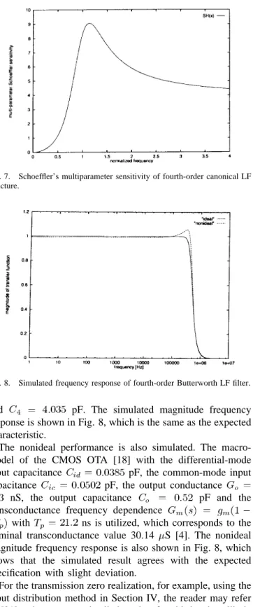
Fig. 8. Simulated frequency response of fourth-order Butterworth LF filter.
and pF. The simulated magnitude frequency
response is shown in Fig. 8, which is the same as the expected characteristic.
The nonideal performance is also simulated. The macro-model of the CMOS OTA [18] with the differential-mode
input capacitance pF, the common-mode input
capacitance pF, the output conductance
nS, the output capacitance pF and the
transconductance frequency dependence
with ns is utilized, which corresponds to the nominal transconductance value 30.14 S [4]. The nonideal magnitude frequency response is also shown in Fig. 8, which shows that the simulated result agrees with the expected specification with slight deviation.
For the transmission zero realization, for example, using the input distribution method in Section IV, the reader may refer to [21], where a very detailed study of a third-order elliptic filter has been presented.
VII. CONCLUSIONS
A general multiple loop feedback approach for the real-ization of OTA-C filters has been proposed. The systematic generation, analysis and design of different filter configurations have been addressed. The method has the following advan-tages: a) it is systematic and general due to the introduction of the feedback matrix and the relationship between
and the feedback connection; b) a variety of new structures with different performances are generated, with both canonical and noncanonical realizations being available; c) all capacitors are grounded and canonical realization can guarantee that all internal nodes have a grounded capacitor; and d) it is also flexible in assigning element values and in various cases simple explicit design formulas are applicable.
We have formulated general relations for all-pole and finite transmission zero realizations. We have also demonstrated the general expressions for sensititvity computation. Using the one-to-one correspondence between the feedback connection matrix and the circuit configuration one can deal with any particular applications based on these general equations. For example, if the circuit topology is known, we may write the feedback matrix and analyze the filtering characteristic and sensitivity performance. For the desired transfer function, on the other hand, an , that is, a circuit structure, may be defined to realize the transfer function. In the paper extensive examples have been given. Although we have concentrated on the demonstration of the powerfulness of the proposed approach in generating high-order OTA-C filter structures, it is very obvious that some first- and second-order filters [3] can also be derived from the general model in Fig. 2.
The performance of multiple loop feedback OTA-C filters taking OTA nonidealities into account should be evaluated. OTA nonidealities may embrace finite input and output imped-ances, frequency dependence of transconductance, noise and nonlinearity of transconductance characteristic. They not only influence the frequency responses and pose stability problems, but also limit the filter dynamic range, as have been discussed in [21].
Noncanonical realization with OTA amplifiers realizing general feedback coefficients can provide some design flex-ibility and results in more useful architectures. However, the noncanonical synthesis produces some nonintegrating nodes (for example, if is realized with an OTA voltage amplifier, there will be a resistive node, which is the inverting input terminal of the th integrator). The parasitic capacitances associated with the node may thus influence the high frequency performance, producing an unwanted pole. More OTA’s also cause other problems as well; the total impact of OTA excess phases will dramatically increase, further degrading the high frequency performance, and larger chip areas and power consumption will also result. Since in the noncanonical re-alization some circuit node may connect more OTA’s, the equivalent node conductance will be enhanced, which may severely deteriorate the low-frequency performance. In both canonical and noncanonical realizations the input capacitance of the integrator OTA will contribute to feedthrough effects (causing unwanted zeros). But in the canonical case it does not cause parasitic poles, since the OTA input capacitance is in a loop containing two circuit capacitances and the number of independent capacitances therefore remains the same.
There exists equivalent transformation of the structures with differential input OTA’s and those with single input OTA’s. Ideally a differential input OTA can be equivalent to two single input OTA’s with the same transconductance value but opposite polarity. As discussed in [21], tradeoffs
between the feedthrough effects (parasitic zeros) caused by some differential input application and the large number of OTA’s due to the single input application must be considered when deciding whether to exploit the differential or single input OTA’s.
Balanced structures using differential input and differen-tial output OTA’s are popular in integrated implementation, which can achieve very high common-mode rejection ratio (CMRR) and reduce both the even-order harmonic distortion components and the effects of the power supply noise. The general unbalanced model in Fig. 2 can be converted into the balanced equivalent by using differential four input and two output OTA’s in integrators and mirroring the feedback network in the upper part to the lower part. All the unbalanced configurations given in the paper can be thus converted into the corresponding balanced counterparts.
REFERENCES
[1] R. Schaumann, M. S. Ghausi, and K. R. Laker, Design of Analog Filters: Passive, Active-RC, and Switched Capacitor. Englewood Cliffs, NJ: Prentice-Hall, 1990.
[2] R. L. Geiger and E. S´anchez-Sinencio, “Active filter design using oper-ational transconductance amplifiers: A tutorial,” IEEE Circuits Devices Mag., pp. 20–32, Mar. 1985.
[3] E. S´anchez-Sinencio, R. L. Geiger, and H. Nev´arez-Lozano, “Generation of continuous-time two integrator loop OTA filter structures,” IEEE Trans. Circuits Syst., vol. 35, pp. 936–946, 1988.
[4] H. Nevarez-Lozano and E. S´anchez-Sinencio, “Minimum parasitic ef-fects biquadratic OTA-C filter architectures,” Analog Integrated Circuits Signal Process., vol. 1, pp. 297–319, 1991.
[5] Y. Sun and J. K. Fidler, “Novel OTA-C realizations of biquadratic transfer functions,” Int. J. Electron., vol. 75, pp. 333–340, 1993. [6] , “Resonator-based universal OTA-grounded capacitor filters,” Int.
J. Circuit Theory Appl., vol. 23, pp. 261–265, 1995.
[7] , “Current-mode continuous-time biquadratic filters based on dual output OTA’s and capacitors,” in Proc. Euro. Conf. Circuit Theory Design, Istanbul, Turkey, Aug. 1995, vol. 2, pp. 805–808.
[8] A. C. M. de Queiroz and L. P. Caloba, “Some design methods of OTA-C and OTA-COTA-CII-ROTA-C active filters,” in Proc. IEE Saraga OTA-Colloquium Dig. Analogue Filters and Filtering Syst., 1993, pp. 1/7–8/7.
[9] R. Nawrocki, “Electronically tunable all-pole low-pass leapfrog ladder filter with operational transconductance amplifier,” Int. J. Electron., vol. 62, pp. 667–672, 1987.
[10] A. C. M. de Queiroz, L. P. Caloba, and E. S´anchez-Sinencio, “Signal flow graph OTA-C integrated filters,” in Proc. IEEE Int. Symp. Circuits Syst., 1988, pp. 2165–2168.
[11] , “Some practical problems in OTA-C filters related with para-sitic capacitances,” in Proc. IEEE Int. Symp. Circuits Syst., 1990, pp. 2279–2282.
[12] R. Nawrocki, “Electronically controlled OTA-C filter with follow-the-leader-feedback structures,” Int. J. Circuit Theory Applicat., vol. 16, pp. 93–96, 1988.
[13] F. Krummenacher, “Design considerations in high-frequency CMOS transconductance amplifier capacitor (TAC) filters,” in Proc. IEEE Int. Symp. Circuits Syst., 1989, pp. 100–105.
[14] Y. Sun and J. K. Fidler, “Canonical realization of high-order all-pole low-pass OTA-C filters,” in Proc. Euro. Conf. Circuit Theory Design, Davos, Switzerland, 1993, pp. 69–72.
[15] , “Minimum component multiple integrator loop feedback OTA-C all-pole filters,” in Proc. Midwest Symp. OTA-Circuits Syst., Lafayette, LA, 1994, pp. 983–986.
[16] Y. Zhang and J. K. Fidler, “A design method for high-order OTA-C low-pass filters with topological structure selection flexibility,” in Proc. Int. Conf. Elec. Measure. Instrum., 1992.
[17] W. Guo, J. Liu, and S. Yang, “The realization of high-order OTA-C filter,” Int. J. Electron., vol. 65, pp. 1153–1157, 1988.
[18] A. P. Nedungadi and R. L. Geiger, “High-frequency voltage-controlled continuous-time lowpass filter using linearized CMOS integrators,” Electron. Lett., vol. 22, pp. 729–731, 1986.
[19] Y. Sun and J. K. Fidler, “High-order current-mode continuous-time multiple output OTA capacitor filters,” in Proc. IEE 15th Saraga Colloq. Digital and Analogue Filters and Filtering Syst., London, England, 1995. [20] , “OTA-C realization of general high-order transfer functions,”
Electron. Lett., vol. 29, pp. 1057–1058, 1993.
[21] , “Performance analysis of multiple loop feedback OTA-C filters,” in Proc. IEE Saraga Colloq. Digital and Analogue Filters and Filtering Syst., London, England, 1994, pp. 9/1–9/7.
Yichuang Sun (M’90) was born in Dalian, China, in 1960. He received the B.S. degree in radio commu-nications and the M.S. degree in radio navigation from Dalian Maritime University, China, and the Ph.D. degree in electronic engineering from the University of York, U.K., in 1982, 1985, and 1996, respectively.
In 1985, he joined Dalian Maritime University, where since 1990, he has been an Associate Profes-sor. He has held a research post at the University of York during the 1995–1996 academic year. He is currently on the staff of the University of Hertfordshire, U.K. His teaching and research interests include analog filter design, analog fault diagnosis, current-mode circuits, analog circuits and signal processing, RF circuits, circuit theory, computer-aided circuit design, and telecommunications and design. He has published more than 70 papers and received a number of awards and honors. His name has been included in three international Who’s Who books.
J. Kel Fidler graduated from King’s College, Durham University, and also the University of Newcastle.
He is Professor of electronics and Pro-Vice-Chancellor at the University of York, U.K., and has held posts at the University of Essex and the Open University. He has more than 30 years of research experience in the area of circuit theory, active and passive filter design, and computer-aided circuit design.
Professor Fidler was a past Chair of the IEE Professional Group E10 (Circuit Theory and Design), and was Chair of the ECCTD’88 Conference in Brighton, England. He is a Fellow of the Institute of Electrical Engineers, U.K.