Reducing Memory Latency by
Improving Resource Utilization
Doctoral thesis
for the degree of philosophiae doctor
Trondheim, June 2010
Norwegian University of Science and Technology
Faculty of Information Technology, Mathematics and
Electrical Engineering
Doctoral thesis
for the degree of philosophiae doctor Faculty of Information Technology, Mathematics and Electrical Engineering
Department of Computer and Information Science c
Marius Grannæs
ISBN 978-82-471-2177-1 (printed version) ISBN 978-82-471-2178-8 (electronic version) ISSN 1503-8181
Doctoral theses at NTNU, 2010:106 Printed by NTNU-trykk
Integrated circuits have been in constant progression since the first prototype in 1958, with the semiconductor industry maintaining a constant rate of miniaturisa-tion of transistors and wires. Up until about the year 2002, processor performance increased by about 55% per year. Since then, limitations on power, ILP and mem-ory latency have slowed the increase in uniprocessor performance to about 20% per year. Although the capacity of DRAM increases by about 40% per year, the latency only decreases by about 6 – 7% per year. This performance gap between the processor and DRAM leads to a problem known as the memory wall.
This thesis aims to improve system memory latency by leveraging available re-sources with excess capacity. This has been achieved through multiple techniques, but mainly by using excess bandwidth and improving scheduling policies.
The first approach presented, destructive read DRAM, changes the underlying assumptions about the contents of a DRAM cell being unchanged after a read. The latency of a read is reduced, but the rest of the memory system requires changes to conserve data.
Prefetching predicts what data is needed in the future and fetches that data into the cache before it is referenced. This dissertation presents a technique for generating
highly accurate prefetches with good timeliness calledDelta Correlating Prediction
Tables (DCPT). DCPT uses a table indexed by the load’s address to store the delta history of individual loads. Delta correlation is then used to predict future
misses. Delta Correlating Prediction Tables with Partial Matching (DCPT-P)
ex-tends DCPT by introducing L1 hoisting which moves data from the L2 to the L1
to further increase performance. In addition, DCPT-P leveragespartial matching
which reduces the spatial resolution of deltas to expose more patterns.
The interaction between the memory controller and the prefetcher is especially im-portant, because of the complex 3D structure of modern DRAM. Utilizing open pages can increase the performance of the system significantly. Memory controllers can increase bandwidth utilization and reduce latency at the same time by schedul-ing prefetches such that the number of page hits are maximized. The interaction between the program, prefetcher and the memory controller is explored.
This thesis examines the impact of having a shared memory system in a CMP. When resources are shared, one core might interfere with another core’s execution by delaying memory requests or displacing useful data in the cache. This effect is quantified and which components are most prone to interference between cores identified. Finally, we present a framework for measuring interference at runtime.
This doctoral thesis was submitted to the Norwegian University of Science and Technology (NTNU) in partial fulfillment of the requirements for the degree phil-osophiae doctor (PhD). The work herein was performed at the Department of Com-puter and Information Science, NTNU, under the supervision of Professor Lasse Natvig.
This thesis consists of two parts. The first part consists of introduction, back-ground, research process, a summary of papers and final conclusions. The second part is the main contribution, presented as a collection of nine research papers.
Acknowledgements
There are many people to whom I am very grateful for their help and encouragement while undertaking the work described in this thesis.
First, I would like to thank my advisor Lasse Natvig for his support, guidance and keeping me on track. He has allowed me to explore this wonderful area of
computer science in the way I wanted. My co-advisors, Professor Mads Nyg˚ard
and Dr. Gaute Myklebust deserves credit for guiding this work, especially in the early phases. Their insights provided much valuable knowledge for completing this thesis.
I would especially like to thank my co-authors: Dr. Haakon Dybdahl, Magnus Jahre and Dr. Per Gunnar Kjeldsberg. Thank you for all the marvellous computer architecture discussions that have led to such wonderful research ideas. Asbjørn Djupdal deserves my gratitude as he did a wonderful job proof-reading the final manuscript for this thesis. I would also like to thank all my coworkers at the Com-plex Systems Section at NTNU: Morten, Dragana, Gunnar T, Gunnar L, Pauline, Kostas, Bjørn-Magnus, Frode, Sigve, Christina, Jan-Christian, Thorvald, Magnus, Nils and Truls.
I would like to thank Professor Per Stenstr¨om for letting me visit Chalmers during
all the people I met there; Martin, Magnus, Wolfgang and Daniel. Thank you for taking so good care of me and making my stay so memorable.
I would like to thank the Faculty of Information Technology, Mathematics and Electrical Engineering and the Department of Computer and Information Science for funding my research. NOTUR provided computational resources which were very valuable for making simulating systems easier and less time-consuming. I would like to thank the HiPEAC European network of excellence. I was fortunate to attended the ACACES summer school on two separate occasions, both of which were very interesting.
I would like to thank my family for inspiring me and supporting me through all these years. Finally, I would like to thank Maria Kristina for her love and support.
Marius Grannæs June 09, 2010
Abstract iii
List of Figures xiii
List of Tables xvi
Abbreviations xix
1 Introduction 1
1.1 The Memory Gap . . . 1
1.2 Analyzing the Memory Hierarchy . . . 2
1.3 Overcoming the Memory Wall . . . 3
1.3.1 Tolerating or Hiding the Memory Gap . . . 3
1.3.2 Increasing Bandwidth Utilization . . . 4
1.3.3 Parallel Throughput-Oriented Architectures . . . 4
1.4 Research Questions . . . 5
1.5 Thesis Outline . . . 5
2 Background 7 2.1 Performance and Fairness Metrics . . . 7
2.1.1 Measuring Performance . . . 7
2.1.2 Aggregating Performance Numbers . . . 9
2.1.3 Multiprogrammed Workload Metrics . . . 9
2.2 Main Memory . . . 10 2.2.1 Memory Cells . . . 10 2.2.2 DRAM Organization . . . 12 2.2.3 DRAM Scheduling . . . 14 2.3 Cache . . . 17 2.3.1 Set-associative caches . . . 17 2.3.2 Cache Misses . . . 18 2.3.3 Replacement Policies . . . 20
2.3.4 Miss Status Holding Registers . . . 20
2.4 Prefetching . . . 20
2.4.1 Sequential Prefetching . . . 21
2.4.3 Address-Based Prefetchers . . . 24
2.4.4 Spatial Locality Prediction . . . 25
2.4.5 Linked Data Prefetchers . . . 26
2.4.6 Adaptive Prefetchers . . . 26
2.4.7 Runahead Execution . . . 27
2.4.8 Software Prefetching . . . 27
3 Research Process and Methodology 29 3.1 Research Process . . . 29
3.1.1 Master Thesis . . . 29
3.1.2 Destructive Read DRAM - Paper I & II . . . 30
3.1.3 Shadow Tags - Paper III . . . 30
3.1.4 Changing Simulators . . . 31
3.1.5 Prewriting . . . 32
3.1.6 Low-Cost Open-Page Prefetch Scheduling - Paper IV . 32 3.1.7 Data Prefetching Championship - Paper V & VII . . . 33
3.1.8 3D Stacking . . . 34
3.1.9 Memory System Interference - Paper VI & VIII . . . . 35
3.1.10 Opportunistic Prefetch Scheduling - Paper IX . . . 36
3.2 Research Methodology . . . 37 3.2.1 Simulators . . . 37 3.2.2 Benchmarks . . . 39 4 Research Contributions 43 4.1 Paper I . . . 43 4.1.1 Abstract . . . 43 4.1.2 Retrospective View . . . 44
4.1.3 Roles of the Authors . . . 44
4.2 Paper II . . . 45
4.2.1 Abstract . . . 45
4.2.2 Retrospective View . . . 45
4.2.3 Roles of the Authors . . . 45
4.3 Paper III . . . 46
4.3.1 Abstract . . . 46
4.3.2 Retrospective View . . . 46
4.3.3 Roles of the Authors . . . 46
4.4 Paper IV . . . 47
4.4.1 Abstract . . . 47
4.4.2 Retrospective View . . . 47
4.4.3 Roles of the Authors . . . 47
4.5 Paper V . . . 48
4.5.1 Abstract . . . 48
4.5.2 Retrospective View . . . 48
4.5.3 Roles of the Authors . . . 49
4.6 Paper VI . . . 49
4.6.2 Retrospective View . . . 49
4.6.3 Roles of the Authors . . . 49
4.7 Paper VII . . . 50
4.7.1 Abstract . . . 50
4.7.2 Roles of the Authors . . . 50
4.8 Paper VIII . . . 50
4.8.1 Abstract . . . 50
4.8.2 Roles of the Authors . . . 51
4.9 Paper IX . . . 51
4.9.1 Abstract . . . 51
4.9.2 Roles of the Authors . . . 52
5 Concluding Remarks 53 5.1 Conclusion . . . 53 5.2 Contributions . . . 54 5.3 Future Work . . . 55 5.4 Outlook . . . 56 Bibliography . . . 57 Papers 71 I Cache Write-Back Schemes for Embedded Destructive-Read DRAM 73 Abstract . . . 75
I.1 Introduction . . . 76
I.2 Embedded Destructive-Read DRAM . . . 77
I.2.1 Embedded Memory . . . 77
I.2.2 Destructive-Read DRAM . . . 78
I.3 New Write-back Schemes . . . 79
I.4 Methodology . . . 82
I.5 Evaluation . . . 84
I.5.1 Initial experiment . . . 84
I.5.2 IPC for Different Write-back Schemes . . . 85
I.5.3 Cache size . . . 87
I.5.4 Latency and number of DRAM banks . . . 88
I.5.5 Write-back Buffer size . . . 88
I.6 Discussion . . . 90
I.7 Related Work . . . 91
I.8 Conclusion . . . 91
Bibliography . . . 92
II Destructive-Read in Embedded DRAM, Impact on Power Consumption 95 Abstract . . . 97
II.1 Introduction . . . 98
II.2.1 Embedded Memory . . . 99
II.2.2 Related Work . . . 99
II.2.3 Destructive-Read DRAM . . . 100
II.2.4 Write-backs . . . 102
II.3 Model for Power Consumption . . . 102
II.3.1 Power model of DRAM with bus . . . 103
II.4 Simulations . . . 105
II.5 Results . . . 106
II.6 Discussion . . . 110
II.7 Conclusions . . . 111
Bibliography . . . 112
III Hardware Prefetching Using Shadow Tagging 115 Abstract . . . 117
III.1 Introduction . . . 118
III.1.1 Contributions . . . 118
III.2 Previous Work . . . 119
III.2.1 Feedback Directed Prefetching . . . 119
III.2.2 Tuning . . . 119
III.2.3 Shadow Tag Directories . . . 120
III.3 Methodology . . . 120
III.3.1 Shadow Tag Controlled Prefetching . . . 120
III.3.2 Prefetch Configuration Selection Heuristic . . . 122
III.3.3 Experimental Setup . . . 123
III.4 Results . . . 124
III.4.1 Bandwidth Usage . . . 126
III.4.2 Sensitivity Analysis . . . 126
III.5 Discussion . . . 128
III.5.1 Parameter Space Exploration . . . 128
III.5.2 Clearing the Shadow Tags . . . 129
III.6 Conclusion . . . 129
Bibliography . . . 129
IV Low-Cost Open-Page Prefetch Scheduling in Chip Multipro-cessors 133 Abstract . . . 135
IV.1 Introduction . . . 136
IV.2 Previous Work . . . 137
IV.2.1 Prefetching . . . 137
IV.2.2 Memory Controllers . . . 137
IV.3 Prefetch Scheduling . . . 138
IV.4 Low cost open page prefetching . . . 139
IV.5 Methodology . . . 140
IV.6 Results . . . 142
IV.6.1 Scheduled Region Prefetching . . . 142
IV.6.3 Insertion policy . . . 143
IV.6.4 Treshold parameter . . . 143
IV.6.5 Quality of Service . . . 144
IV.7 Discussion . . . 145
IV.8 Conclusion . . . 146
Bibliography . . . 146
V Storage Efficient Hardware Prefetching using Delta Corre-lating Prediction Tables 149 Abstract . . . 151
V.1 Introduction . . . 152
V.2 Previous Work . . . 152
V.2.1 Reference Prediction Tables . . . 152
V.2.2 PC/DC Prefetching . . . 153
V.3 Delta Correlating Prediction Tables . . . 154
V.4 Methodology . . . 155 V.5 Results . . . 155 V.5.1 DCPT Parameters . . . 157 V.6 Discussion . . . 158 V.7 Conclusion . . . 159 Bibliography . . . 160
VI A Quantitative Study of Memory System Interference in Chip Multiprocessor Architectures 163 Abstract . . . 165
VI.1 Introduction . . . 166
VI.2 Related Work . . . 168
VI.3 Methodology . . . 169
VI.3.1 Chip Multiprocessor Architectures . . . 169
VI.3.2 Measuring and Reporting Interference . . . 169
VI.3.3 Processor Model Scaling . . . 171
VI.3.4 Simulation Methodology . . . 172
VI.4 Results . . . 174
VI.5 Conclusion and Further Work . . . 179
Bibliography . . . 180
VII Multi-Level Hardware Prefetching using Low Complexity Delta Correlating Prediction Tables with Partial Matching 183 Abstract . . . 185
VII.1 Introduction . . . 186
VII.2 Previous Work . . . 186
VII.3 Delta Correlating Prediction Tables . . . 188
VII.3.1 Overview . . . 188
VII.3.2 DCPT-P Implementation . . . 189
VII.3.3 L1 Hoisting . . . 192
VII.4 Methodology . . . 194
VII.5 Results . . . 194
VII.5.1 Area and performance trade-offs . . . 197
VII.6 Discussion . . . 199
VII.7 Conclusion . . . 201
Bibliography . . . 201
VIII DIEF: An Accurate Interference Feedback Mechanism for Chip Multiprocessor Memory Systems 205 Abstract . . . 207
VIII.1 Introduction . . . 208
VIII.2 Background . . . 209
VIII.2.1Interference Definition and Metrics . . . 209
VIII.2.2Modern Memory Bus Interfaces . . . 210
VIII.3 Shared Memory System Latency Taxonomy . . . 210
VIII.4 The Dynamic Interference Estimation Framework . . . 212
VIII.4.1Estimating Private Memory Bus Latency ( ˆLmt, ˆLmq and ˆLme) . . . 213
VIII.4.2Estimating Cache Capacity Interference ˆIcc . . . 217
VIII.4.3Estimating Interconnect Interference ( ˆIie, ˆIiq, ˆIit and ˆ Iid) . . . 217 VIII.5 Methodology . . . 218 VIII.6 Results . . . 218 VIII.6.1Estimation Accuracy . . . 219 VIII.6.2DIEF Parameters . . . 222
VIII.7 Related Work . . . 222
VIII.8 Conclusion . . . 224
Bibliography . . . 224
IX Exploring the Prefetcher/Memory Controller Design Space: An Opportunistic Prefetch Scheduling Strategy 227 Abstract . . . 229
IX.1 Introduction . . . 230
IX.2 Related Work . . . 231
IX.2.1 Prefetching . . . 231
IX.2.2 Memory Controllers . . . 231
IX.3 Prefetch Scheduling Strategies . . . 232
IX.3.1 Opportunistic Prefetch Scheduling . . . 233
IX.4 Methodology . . . 233
IX.5 Results . . . 235
IX.5.1 Performance . . . 235
IX.5.2 Maximum Performance Regression . . . 236
IX.5.3 Accuracy and Coverage . . . 237
IX.5.4 Increasing DRAM Bandwidth . . . 238
IX.6 Discussion . . . 239
List of Figures
1.1 Development of CPU performance versus memory latency . . . . 2
1.2 Size of the last level on-die cache as a function of year of intro-duction for some Intel microprocessors . . . 3
2.1 Schematic diagram of a single DRAM cell. . . 11
2.2 Schematic diagram of a single CMOS SRAM cell. . . 12
2.3 Organization of DRAM. . . 13
2.4 DRAM latency as a function of bandwidth for common consumer-grade main memory technologies . . . 14
2.5 Example of a memory hierarchy with 2 levels of cache. . . 17
2.6 Cache access time and energy as a function of size . . . 18
2.7 Organization of a 4K two-way set associative cache with 64B cache lines. . . 19
2.8 Conceptual MSHR entry . . . 20
2.9 Format of a Stride Directed Prefetching entry. . . 23
2.10 Format of a Reference Prediction Table entry. . . 23
2.11 Construction of the delta table in PC/DC. . . 24
I.1 A logical sketch of a DRAM macro. . . 78
I.2 Conceptual waveform diagrams of conventional DRAM architec-ture vs. destructive-read . . . 78
I.3 Conceptual view of DRAM. . . 79
I.4 Example of execution with the two different write-back schemes 81 I.5 The simulated computer. . . 82
I.6 Source code for the initial experiment. . . 84
I.7 Results from the initial experiment. . . 85
I.8 Performance of baseline configuration for different SPEC2000 benchmarks. . . 86
I.9 Speedup in terms of increased IPC. . . 87
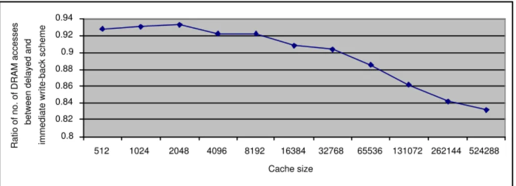
I.10 Comparison of the total number of accesses to DRAM from caches for the two different write-back schemes . . . 88
I.11 Average IPC as a function of latency . . . 89
I.12 Average IPC as a function of the number of DRAM banks and buffer size . . . 89
II.1 Multiple cores and memory in a single chip. . . 98
II.2 Inside a DRAM bank. . . 99
II.3 Conceptual waveform diagrams of conventional DRAM architec-ture vs. destructive-read . . . 101
II.4 Conceptual view of DRAM. . . 101
II.5 IPC for the applications in the SPEC2000 benchmark suite . . . 103
II.6 Data communication when accessing a memory bank. . . 104
II.7 The simulated single chip computer. . . 106
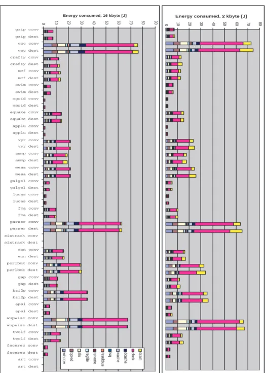
II.8 Energy consumption for various applications in the SPEC2000 suite . . . 107
II.9 Energy consumption for gcc . . . 108
II.10 Number of DRAM accesses per clock cycle for 16 kbytes cache . 108 II.11 Number of clock cycles and energy consumption for Ammp, Art and Twolf . . . 109
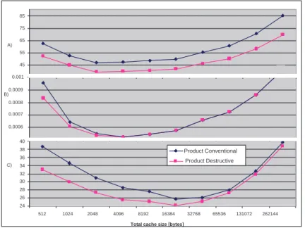
II.12 Product of execution time and energy consumption for Ammp, Art and Tworlf . . . 110
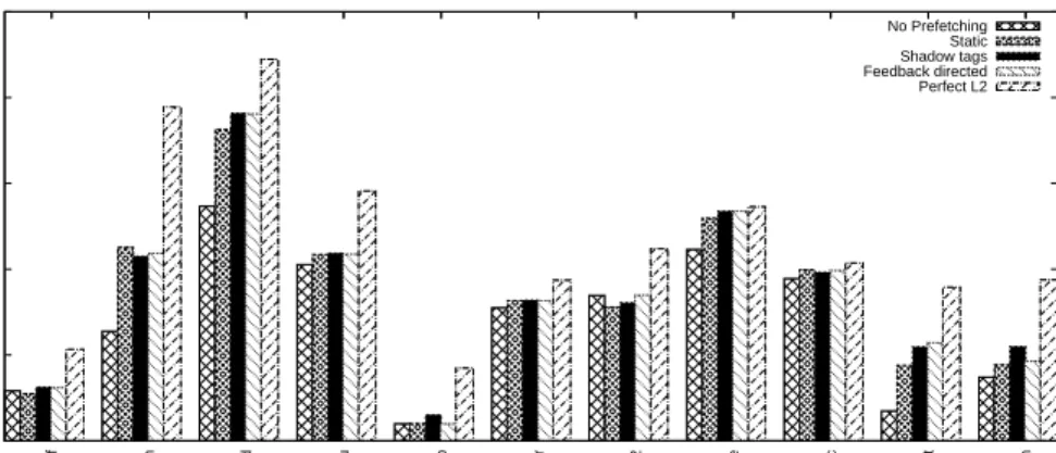
III.1 The proposed architecture. The L1 cache is connected to both the L2 cache and the shadow tag directory. The controller evalu-ates the performance of the two configurations and reconfigures the prefetchers accordingly. . . 121
III.2 Performance of dynamic parameter selection on static prefetching.124 III.3 Performance of dynamic parameter selection on C/DC prefetching.125 III.4 Performance of dynamic parameter selection on RPT prefetching. 126 III.5 Number of main memory accesses for different combinations of prefetching heuristics and parameter selection methods. Values are normalized to no prefetching. . . 127
III.6 Performance of shadow tag prefetching as a function of param-eters to the heuristic. . . 127
III.7 Performance of shadow tag prefetching as a function of the band-width threshold parameter. . . 128
IV.1 The 3D structure of modern DRAM. . . 136
IV.2 Prefetch scheduling policies . . . 139
IV.3 IPC improvement as a function of accuracy . . . 140
IV.4 Speedup in IPC relative to no prefetching using a FR-FCFS memory controller. . . 142
IV.5 Average speedup in IPC relative to no prefetching. . . 143
IV.6 Effects of insertion policy on average IPC speedup. . . 144
IV.7 IPC improvement as a function of treshold . . . 144
IV.8 Maximum IPC degradation for any thread as a function of work-loads. . . 145
V.1 Format of a Reference Prediction Table entry. . . 153
V.2 Example of a Global History Buffer. . . 153
V.4 Speedup compared to no prefetching. 2 MB L2 cache with
un-limited bandwidth. . . 156
V.5 Speedup compared to no prefetching. 2 MB L2 cache with lim-ited bandwidth. . . 156
V.6 Speedup compared to no prefetching. 512KB L2 cache with limited bandwidth. . . 156
V.7 Coverage and speedup as a function of the number of bits used to represent a delta. . . 158
V.8 Speedup vs. the number of deltas per entry. . . 159
V.9 Speedup vs table size. . . 160
VI.1 Performance Impact of Interference in the 4-core, Crossbar-Based CMP with 4 Memory Channels . . . 167
VI.2 Crossbar-based CMP . . . 167
VI.3 Ring-based CMP . . . 168
VI.4 Interference Measurement Workflow . . . 171
VI.5 4-core Fairness Metric Values . . . 177
VI.6 Interference Impact Breakdown . . . 177
VI.7 4-core CMP Interference Impact (cores-interconnect-channels) . 178 VI.8 16-core Ring Interference Impact . . . 178
VII.1 Format of a single DCPT-P entry. . . 188
VII.2 Impact of increasing the numbers of bits used to represent a delta.189 VII.3 Position in the circular buffer where a match is found. . . 190
VII.4 DCPT-P Pipeline . . . 191
VII.5 Pattern matching implementation. . . 191
VII.6 Speedup of Sphinx as a function of LSB masked in partial match-ing. . . 193
VII.7 2 MB L2 cache. Benchmarks with large speedups. . . 195
VII.8 2 MB L2 cache. Benchmarks with small speedups. . . 195
VII.9 512KB L2 cache. Benchmarks with large speedups. . . 196
VII.10 512KB L2 cache. Benchmarks with small speedups. . . 196
VII.11 Breakdown of performance contribution of DCPT-P. Benchmarks with large speedups. . . 197
VII.12 Breakdown of performance contribution of DCPT-P. Benchmarks with small speedups. . . 197
VII.13 Average speedup as a function of the number of deltas in each entry . . . 198
VII.14 Average speedup as a function of the number of table entries . . 198
VII.15 Distribution of the number of deltas registered in a table entry upon replacement. . . 199
VIII.1 Dynamic Interference Estimation Framework (DIEF) Architecture212 VIII.2 Private Memory Bus Emulation . . . 213
VIII.3 Memory Bus Queue and Transfer Latency Estimation Example . 215 VIII.4 Relative Estimation Errors and Number of Estimates . . . 219
VIII.7 4-core Bus Queue Error . . . 221
VIII.8 Root Mean Squared Error. 8-core CMP Sample Size Accuracy Impact . . . 221
VIII.9 Average Latency Between Estimates. 8-core CMP Sample Size Accuracy Impact . . . 222
VIII.10 4-core Page Locality Factor . . . 223
VIII.11 4-core Bus Buffer Size . . . 223
IX.1 3D structure of DRAM. . . 230
IX.2 Average speedup for all cores over all workloads for different scheduling strategies and prefetchers. . . 236
IX.3 Lowest speedup for any core in any workload for different sch-eduling strategies and prefetchers. . . 236
IX.4 Average accuracy for all workloads. . . 237
IX.5 Average coverage for all workloads. . . 237
IX.6 Effect of increasing the amount of bandwidth available on se-quential prefetching. . . 238
IX.7 Effect of increasing the amount of bandwidth available on RPT prefetching. . . 239
List of Tables
II.1 Random cycle time for various memories [11]. . . 100III.1 The simulation parameters used with SimpleScalar. . . 123
IV.1 Processor Core Parameters . . . 141
IV.2 Memory System Parameters . . . 141
IV.3 Multiprogrammed Workloads . . . 146
V.1 Example delta stream. . . 154
VI.1 Shared Memory System Latency Breakdown . . . 170
VI.2 Architecture Parameter Scaling . . . 172
VI.3 Cache Parameters (4-core/8-core/16-core) . . . 172
VI.4 Processor Core Parameters . . . 173
VI.6 Randomly Generated 4-core Multiprogrammed Workloads . . . . 174
VI.7 Randomly Generated 8-core Multiprogrammed Workloads . . . . 175
VI.8 Randomly Generated 16-core Multiprogrammed Workloads . . . 176
VII.1 Example delta stream. . . 190
VIII.1 Memory System Latency Taxonomy . . . 211
VIII.2 Status Bits . . . 214
VIII.3 Lˆmt Estimates . . . 214
VIII.4 CMP Models . . . 218
IX.1 Example Page Vector Table showing a strided prefetch pattern for page address 100. . . 233
IX.2 Processor Core Parameters . . . 234
IX.3 Memory System Parameters . . . 234
AMPM Access Map Pattern Matching
API Application Programming Interface
AWS Aggregated Weighted Speedup
C/DC CZone/Delta Correlation
CDP Content-Directed Prefetching
CMP Chip Multi-Processor
CPU Central Processing Unit
DCPT Delta Correlating Prediction Tables
DCPT-P Delta Correlating Prediction Tables with Partial Matching
DDR Double Data Rate
DPC Data Prefetching Championship
DRAM Dynamic Random Access Memory
EDP Energy Delay Product
ED2P Energy Delay Squared Product
eDRAM Embedded Dynamic Random Access Memory
FCFS First-Come First-Served
FIFO First In, First Out
FR-FCFS First-Ready First-Come First-Served
GA Genetic Algorithms
GHB Global History Buffer
GHB-LDB Global History Buffer - Local Delta Buffer
ICCD International Conference on Computer Design
ILP Instruction Level Parallelism
IPC Instructions Per Cycle
IQ Instruction Queue
ITRS International Technology Roadmap for Semiconductors
JILP Journal of Instruction-Level Parallelism
LRU Least Recently Used
MSHR Miss Status Holding Register
MLP Memory Level Parallelism
NFQ Network Fair Queuing
NUCA Non-Uniform Cache Architecture
OoO Out-of-Order
PC Program Counter
PC/DC Program Counter/Delta Correlation Prefetching
PDFCM Prefetching based on a Differential Finite Context Machine
PVT Page Vector Table
RL Reinforcement Learning
ROB Reorder Buffer
RPT Reference Prediction Tables
SDP Stride Directed Prefetching
SMS Spatial Memory Streaming
SMT Simultaneous Multithreading
SRAM Static Random Access Memory
TCP Tag Correlating Prefetching
TLB Translation Lookaside Buffer
TMS Temporal Memory Streaming
TPS Transactions Per Second
WAM Weighted Arithmetic Mean
Introduction
There is an old network saying: Bandwidth problems can be cured with money. Latency problems are harder because the speed of light is fixed – you can’t bribe God.
– Anonymous
1.1
The Memory Gap
Each year exponentially more transistors can be put into a single integrated cir-cuit [57, 99]. Moore’s law is the empirical observation that the number of transistors that can be placed on an integrated circuit, with respect to minimum component cost, will double every 24 months. Increased transistor density, in turn, translates into faster computers for consumers.
Up until about the year 2002, processor performance increased by about 55% per
year [47]. Since then, limitations on power,Instruction Level Parallelism (ILP)and
memory latency have slowed the increase in uniprocessor performance to about 20%
per year. Although the capacity of Dynamic Random Access Memory (DRAM)
increases by about 40% per year, the latency only decreases by about 6-7% per year [111]. This gap between the processor and DRAM leads to a performance
problem known as the“memory wall”(or“memory gap”) [149]. Figure 1.1 shows
the relative uniprocessor performance versus memory latency.
The most important technique in overcoming the memory wall was the introduc-tion of caches in the memory hierarchy [47, 128]. Caches were first introduced in literature in 1968 in a description of the memory system in a IBM Model 85 [137]. Caches are smaller and faster memories which exploits spatial and temporal lo-cality. Spatial locality is the tendency for programs to access data that is close in address space, for example instructions. Temporal locality is the tendency for programs to access the same data repeatedly. Examples include: read-modify-write
1 10 100 1000 10000 100000 1980 1985 1990 1995 2000 2005 2010 Performance Year CPU performance Memory performance
Figure 1.1: Development of CPU performance versus memory latency [47].
cycles and single variables in tight loops. These observations can be exploited by moving recently used data closer to the processor. This makes it faster to access data on average, which in turn speeds up overall computation. The importance of this technique is clearly shown in figure 1.2 where the size of the cache is plotted as a function of the year of introduction for some Intel processors.
1.2
Analyzing the Memory Hierarchy
Equation 1.1 shows a simplified1 analytical model to calculate the overall system
latency given a single level cache memory hierarchy. For a more complete analytical model see Jacob et al. [63].
Lsystem=Lcache+pmiss·(Lmain memory+Lcongestion) (1.1)
In this equation Lsystem is the overall memory system latency as observed by the
processor. DecreasingLsystemcan thus increase overall system performance. Lcache
is the latency of the cache. pmissis the probability that the data is not found in the
cache. If the data is not found in the cache, then the data is found in main
mem-ory. The latency of main memory consists of two components: Lmain memory is the
minimum time to transfer data over the memory bus. Additionally, modern
proces-sors (orChip Multi-Processors (CMPs)) can issue multiple memory requests that
can be serviced concurrently which can cause congestion, which in turn increases
latency (Lcongestion).
1This model assumes no virtual memory and infinite cache bandwidth. In addition, in most
1 10 100 1000 10000 1985 1990 1995 2000 2005 2010 Cache size (kB) Year 80486DX Pentium Pentium Pro
Pentium II Pentium IIIPentium 4
Pentium 4E Core 2
Core i7
Figure 1.2: Size of the last level on-die cache as a function of year of introduction for some Intel microprocessors. Note that only one cache size is shown per processor. In practice Intel varies the amount of cache on a processor as a way to differentiate products and to enhance yield [147].
1.3
Overcoming the Memory Wall
To increase memory system performance there are three main strategies: Tolerating or hiding the latency, increasing bandwidth utilization and moving to a parallel throughput-oriented architecture (CMPs).
1.3.1
Tolerating or Hiding the Memory Gap
Naturally, because of the importance of the memory system in achieving high performance several techniques have been developed to decrease or tolerate the memory system latency. Using a memory hierarchy of caches is a technique that hides the memory latency from the processors viewpoint. Although access to main memory is slow, in most cases the data that is needed will be in a faster cache. Prefetching or speculative loads, i.e. moving data from main memory to caches speculatively, can hide more of main memory latency [47]. Scratchpad memory makes the programmer explicitly move data from main memory to faster stor-age [8], which can increase performance. The Cell processor uses such an approach where each processor core has a relatively small local storage area [72, 79, 148]. Because cache misses will occur, it is important to be able to tolerate these events
and, if possible, continue execution. Out-of-Order (OoO) execution allows the
processor to continue execution of instructions which do not depend on the load [47]. By using caches that can handle multiple concurrent misses (lock-up free) the processor can then issue multiple loads that might also miss in the caches while waiting for the original load to complete [116].
In most operating systems, the processor will schedule another thread if it is stalled
waiting for a long I/O operation. Simultaneous Multithreading (SMT) takes this
further by allowing multiple threads to execute on the same core [141]. If one core stalls because of a load, the other threads will be able to continue execution. The UltraSPARC T1 (“Niagara”) processor uses up to eight cores which can process four threads simultaneously [77]. This adds up to a total of 32 concurrent threads. The idea is that by having a large number of concurrently executing threads, stalling is minimized.
1.3.2
Increasing Bandwidth Utilization
Overall, the amount of off-chip communication is limited by the number of pins
on the chip package [52]. In the short term (2007-2015) International Technology
Roadmap for Semiconductors (ITRS)projects that the number of pins will increase by only 7% p.a. [57]. Because the number of transistors per chip increases much faster, this results in that the number of transistors per pin increases exponentially. This in turn increases the bandwidth requirements per pin.
To meet this demand for increased bandwidth, a variety of techniques have been employed. DRAM interfaces have moved from asynchronous to synchronous with fast page buffers. The fast page buffers holds the most recently used data in a
faster access buffer to exploit the same spatial locality as caches. Double Data
Rate (DDR) memory was introduced to further increase effective bandwidth by transferring data on both edges of the DRAM clock signal. These techniques have all increased bandwidth by a significant amount, but at the expense of higher latency [47]. In addition, these advances have increased the complexity of the DRAM interface, thus increasing the interest in DRAM scheduling policies [119]. In particular, scheduling decisions can effect the utilization of the memory bus by prioritizing requests that can utilize the fast page buffer (page hits). Furthermore, by speculatively prefetching data into the cache, a lower latency can be traded for higher bandwidth usage.
1.3.3
Parallel Throughput-Oriented Architectures
Recently, there has been a shift in the industry from uniprocessors to CMPs. A CMP is multiple processor cores in a single package [109]. This shift is partially due to the memory gap, but equally important is the limits on ILP, power dissi-pation and design complexity. This also marks a shift in programming paradigms. To achieve maximum performance, a parallel implementation of the application is required [112]. Additionally, this shifts the focus away from single-threaded perfor-mance to system throughput. However, due to Amdahl’s law [47], there are limits to the maximum speedup achievable by having a parallel implementation as some portions of the code are bound to be sequential. In practice, some applications are more difficult to parallelize than others. Webservers or search engines are typical
examples of programs that can easily be made parallel as each client can use a separate thread and there are typically more users than cores available. Other ap-plications are harder to parallelize, because of dependencies between computations that forces serialization, such as long pointer-chains. In this context, there are two optimization goals: reducing the overall memory latency for the serial portion and increasing memory throughput and decreasing latency in the parallel portion.
1.4
Research Questions
The main research question for this thesis is:
How, and at what cost, can memory system latency be reduced by im-proving resource utilization?
This question can be subdivided further according to equation 1.1 into the following subquestions:
1. How can excess memory bandwidth be utilized to achieve a lowermaximum
memory latency (Lmain memory) ?
2. How can excess memory bandwidth be utilized to achieve a lower average
memory latency (pmiss) ?
3. How does scheduling decisions in modern highly parallel and complex DRAM
interfaces affect the bandwidth/latency trade-off (pmissandLcongestion) ?
4. How does interference in the shared memory system affect Chip
Multiproces-sor performance (Lcongestion) ?
1.5
Thesis Outline
The remainder of this thesis is organized as follows: Chapter 2 contains background information regarding measuring performance, DRAM, caches and prefetching. Chapter 3 describes the research process, introduces each paper, describes the simulators used and the methodology. Each paper is described in chapter 4 with a breakdown of the roles of each author and a retrospective view (where applicable). Chapter 5 concludes the thesis with a summary of contributions, some thoughts on future work and an outlook. The appendix holds each paper I have authored or coauthored in chronological order. These papers are reproduced faithfully with regard to the published text, but has been reformatted to increase readability.
Background
Those who don’t know history are doomed to repeat it.
– Edmund Burke
2.1
Performance and Fairness Metrics
2.1.1
Measuring Performance
Measuring performance is a tricky task even for a single processor system. The ideal measure of performance is the wall clock time needed to complete a compu-tation [47, 129]. “Completing a compucompu-tation” can have different meanings from a
user and a system perspective. A user is often interested in theresponse timeof the
system. That is the time it takes from the user issues a request to the completion of that request. The system has a different, and perhaps conflicting, view. In the
system view the objective is to maximize the overall throughput. Throughput is a
measure of the amount of computation performed by the system as a whole during a time interval. These two views can be conflicting, because the system might opt to delay one task (thus increasing that task’s response time) in order to prioritize some other task, which would in turn increase throughput.
However, measuring wall clock time is not always practical. This is especially true when simulating a computer system where running an entire benchmark suite to
completion could take several weeks. Thus, Instructions Per Cycle (IPC) is often
used as a proxy for overall performance. The IPC of a system can often be measured directly through performance counters, which are present in most modern high-performance processors [14]. In practice architects often simulate a portion of the benchmark and measure the IPC during that portion of the benchmark. Another approach is to reduce the dataset, which in turn reduces simulation time [150].
Such an approach can lead to non-representative performance measurements due to phase changes in program behaviour. This effect can be mitigated through the use of Simpoints [113]. Simpoints uses a statistical model to select several represen-tative points in the program execution and aggregates the results from several such points. A related approach is used by the SMARTS system [150]. SMARTS uses random samples and uses statistics to determine when the measurements converge and thus stop simulating.
IPC can be misleading as an indicator of performance in situations where a program can commit instructions, but fail to make forward progress. This is especially true in multi-threaded applications where threads can be waiting in a spinlock. A spinlock is often implemented as a tight loop which a modern processor can execute very quickly in terms of IPC. In this case, IPC will be high, but the actual work that is performed is none. This has lead to the development of more
work-oriented metrics such asTransactions Per Second (TPS), where the number
of useful (database-)transactions per second is measured.
In practice, one is often more interested in the speedup that is achieved by using a
certain technique rather than raw IPC numbers. Speedup is calculated according
to equation 2.1 [47]. In this equationnew refers to the enhanced system, whileold
refers to a system without the enhancement.
Speedup = Execution Timeold
Execution Timenew
(2.1)
If the same program with the same dynamic instructions are run and with the same clock frequency, then equation 2.1 can be rewritten to include IPC as shown in equation 2.2.
Speedup = Execution Timeold
Execution Timenew
=IPCnew
IPCold
(2.2)
In recent years there has been an increased interest in reducing the amount of power required by the processor. This interest has been sparked by the increasing number of mobile devices, which are powered by batteries. Therefore, decreasing the power requirements of the processor increases the life-time of the device considerably. In addition, as processors dissipate more power, the core temperature increases. To keep processors stable, significant cooling is required, which adds to the overall operating cost of the system [9].
It is possible to measure power (P) directly, but this is often not a very useful metric by itself as it does not give any indication of the computational performance.
A more useful metric is the Energy Delay Product (EDP). This metric has an
equal balance between the energy requirements and the performance of the system. However, the problem with EDP is that because it favors energy and performance equally, the metric favors small and slow processors, because power consumption
increases more than linearly with performance. Thus, the delay is often squared
(ED2P) or cubed (ED3P) thus increasing the emphasis on performance [43].
2.1.2
Aggregating Performance Numbers
To properly characterize an architectural technique it must be simulated on a wide range of programs in order to ensure that the proposed technique applies to a broad range of applications, rather than exploiting a feature of a particular program. This is often achieved through using a benchmark suite which is comprised of several benchmarks. It is often useful to aggregate the performance results from the entire benchmark suite into a single number.
The simplest approach is to use Weighted Arithmetic Mean (WAM) as shown in
equation 2.3. In this equation a measurement of programiis denoted byMi. Each
program is given a weight (ωi) which can be adjusted according to user preference
(program execution time, program importance in day-to-day use, etc.). Typically, when running experiments with a fixed number of cycles per benchmark WAM can be used with equal weights to measure average IPC [68].
WAM = 1 n n X i=1 ωi·Mi (2.3)
Another possibility is to use theWeighted Harmonic Mean (WHM)which is shown
in equation 2.4. This metric is typically useful when aggregating rates [68, 129].
WHM = Pnn
i=1
ωi
Mi
(2.4)
The third option is the geometric mean shown in equation 2.5. The use of the geometric mean is discouraged by several researchers [62, 68, 129]. The problem with the use of the geometric mean is that it is less useful as an predictor of actual performance [129]. Furthermore, it is harder to visualize than the harmonic and arithmetic mean, because it uses an n-dimensional space.
G= n v u u t n Y i=1 Mi (2.5)
2.1.3
Multiprogrammed Workload Metrics
In a multiprocessor or Chip Multi-Processor (CMP) it is possible to increase the
performance of one thread at the expense of another. One thread might use a dis-proportional amount of shared resources, such that a second thread’s performance
suffers. To measure this effect it is convenient to use a fairness metric such as the one proposed by Gabor et.al. [37, 41], as shown in equation 2.6.
Fairness = min j,k Speedup j Speedupk = min j,k IPCM P j IPCAlone j IPCMP k IPCAlone k (2.6)
In this metric the speedup1 for every core/processor is computed relative to the
performance of that core running alone in the system (i.e. no sharing of resources). A fairness value of 1 indicates that all cores have equal speedup, while 0 indicates that at least one core is not making forward progress.
Furthermore, optimizing for this fairness metric alone is meaningless as it is easy to slow down every thread such that this metric approaches 1. Instead, this metric
must be coupled with a performance metric, such asAggregated Weighted Speedup
(AWS) or Harmonic Mean of Speedups (HMS) [41, 92, 130]. AWS2 is defined as [130]: AWS = n X i=1 Speedupi = n X i=1 IPCMPi IPCAlonei (2.7)
Where nis the number of processors/cores in the system and the speedup is
cal-culated compared to a baseline where the core does not compete for resources (i.e. the other cores are idle).
HMS is defined as [92]: HMS =Pn n i=1 1 Speedupi (2.8)
2.2
Main Memory
2.2.1
Memory Cells
Dynamic Random Access Memory (DRAM) is the most common technology used to implement main memory. To store a single bit of information, a capacitor and transistor is used as shown in figure 2.1. Such a DRAM cell works by storing a
charge in the capacitor (CB) [48]. If the storage capacitor (CB) is charged to the
supply voltage (VDD) then the cell stores a 1. To access the data the cell transistor
1In practice, there will be a slowdown, because the performance of running alone in the system
is higher.
2The weight in AWS and HMS is not explicit in these equations. The weight is inversely proportional to IPC. Lower IPC threads will get a higher speedup compared to high IPC threads with an equal increase in the number of committed instructions.
DRAM Cell Row Select Q 1
CB C L
To Sense Amplifiers
Figure 2.1: Schematic diagram of a single DRAM cell.
(Q1) must be switched on. Because the sense line is comparatively large it has a
capacitance (CL) significantly larger thanCB. Thus the change in voltage in the
sense line is comparatively small according to equation 2.9.
∆v=VDD
CB
CB+CL
(2.9)
This small voltage change is amplified by sense amplifiers at the end of the sense line. After the data has been read, the sense lines must be returned to their neutral state such that charge transferred to the sense lines does not interfere with later
reads. This action is normally known asprecharging. The capacitorCBwill slowly
leak its charge over time due to leakage. In order to preserve data the cell contents
must be read and then rewritten periodically by the system (refresh). This interval
is typically in the order of once per millisecond [48]. The performance impact of refreshing can be neglible by using techniques to mask this periodic operation [42].
Static Random Access Memory (SRAM), on the other hand, is made entirely in
transistors as shown in figure 2.2. The cell can be in two stable states: Either Q1
and Q4 are active, or Q2and Q3 are active. In this figure the two transistorsQA
control access to the data stored in the cell, in a similar manner asQ1 for DRAM
cells. Because SRAM uses six transistors per bit, while DRAM only requires one transistor and a capacitor per bit, SRAM requires six to eight times as much area as DRAM [96]. SRAM has three advantages compared to DRAM: It has lower latency than DRAM, no need for refresh and can be built in the same logic-process used by high-performance processors. Thus, SRAM is often used for on-chip caches.
Embedded Dynamic Random Access Memory (eDRAM) offers a compromise. It uses a similar cell as regular DRAM. However, eDRAM can be integrated with the processor, because it uses the same logic-based process used in high-performance processors [61]. The use of a non-optimized process for eDRAM results in increased area requirements per bit, but the requirement is still much less than for SRAM [96]. This has led some researchers to investigate the possibility for using eDRAM as
Q4 Q2 Q1 Q3 VDD D D Row Select QA QA
Figure 2.2: Schematic diagram of a single CMOS SRAM cell. Note that it is possible to construct other types of SRAM cells using other technology and number of transistors.
on-chip caches [139], scratchpad memory [8], or main memory [88].
Recently, 3D stacking has become an option for integrating DRAM on a chip. 3D stacking is a technique where multiple dies are stacked on top of each other and inter-die vias connect them [26, 88, 115]. This technique has two major advan-tages. First, it reduces average wire latency, because the dies are typically very close. Secondly, because the dies can be produced separately, each die can be produced in different production technologies, thus enabling mixing high-density DRAM processes with high performance logic processes [12].
2.2.2
DRAM Organization
In order to store more than a single bit, DRAM cells are organized in a matrix as shown in figure 2.3. The row address is first decoded into activating a single row in the matrix (Row Select). This in turn activates all DRAM cells in that row. Each DRAM cell outputs its content into the corresponding bit lines, which in turn is amplified by the sense amplifiers. Finally, the column decoder selects the relevant bits and the data is transferred to the processor.
The matrix organization at the core of DRAM has changed very little over the past couple of decades. However, there has been a number of significant improvements in the interface to the matrix. The most significant improvements are fast page
mode, synchronous transfer andDouble Data Rate (DDR) transfer [47]. However,
as shown in figure 2.4 these improvements have for the most part improved memory bandwidth, rather than reduced memory latency [111].
Figure 2.3: Organization of DRAM.
2.2.2.1 Fast Page Mode
Most programs exhibit spatial locality. Spatial locality is the tendency for programs to access data that are close in address space. To improve performance multiple columns are read by the sense amplifiers and stored in a row buffer [22]. Accessing data in this row buffer has a much lower latency as it bypasses the need for the original data from the DRAM cells. An access to data that is located in this buffer
is often referred to as apage hit. In contemporary DRAM this row buffer is typically
1-8KB large.
The contents of this buffer is controlled by the memory controller. Leaving data in the buffer blocks the precharging of the bit lines, because the buffer is closely tied to the sense amplifiers. Thus, the memory controller has to make a trade-off between leaving the data in the buffer (open page policy ) and precharging the bit lines (closed page policy) [2]. The open page policy lowers latency if there is a page hit. Conversely, the closed page policy lowers the latency if there is a page miss. Thus, the best policy depends on the amount of spatial locality in the execution of the program.
2.2.2.2 Synchronous DRAM
Up until early 1997, all DRAM was asynchronous [98]. In an asynchronous design
there is no central clocking common to both the DRAM and the Central
Process-ing Unit (CPU). Instead, the bus was designed to use timing constraints and/or timing strobes. In particular, the CPU had to wait for one memory transfer to com-plete before issuing another memory request. Using a synchronous design (where the processor and DRAM module use a single master clock) made it possible to pipeline requests to different DRAM banks. A bank is essentially another DRAM matrix, which can be independently accessed (though multiple banks may share
0 50 100 150 200 250 300 350 1 10 100 1000 10000 100000 Latency (ns) Bandwidth (MB/s) DRAM (1980)
Page Mode DRAM (1983)
Fast Page Mode DRAM (1986)
Fast Page Mode DRAM (1993) Synchronous DRAM (1997)DDR SDRAM (2000)
DDR2 SDRAM (2003)DDR3 SDRAM (2007) DDR3-1600 SDRAM (2009)
Figure 2.4: DRAM latency as a function of bandwidth for common consumer-grade main memory technologies [111, 146].
the same memory bus). Additionally, a synchronous design removed the need for timing strobes, which reduces latency [22]. Overall, this technique reduced latency dramatically, while increasing throughput at the same time.
2.2.2.3 Double Data Rate
The third major innovation in DRAM technology was the introduction of DDR
DRAM. In DDR DRAM data is transferred on both edges of the clock, thus
effectively doubling the bandwidth to main memory [25, 98].
2.2.3
DRAM Scheduling
DRAM controllers have typically served memory requests in a Come
First-Served (FCFS) manner. Because of the increased complexity and parallelism in modern DRAM it is possible to increase performance or enforce memory fairness by reordering requests [104, 119]. Memory scheduling is currently a very active research field. The research focuses mostly on five distinct areas: Exploiting open pages, prioritizing critical loads, minimizing bank conflicts, increasing fairness and prefetch scheduling.
2.2.3.1 Increasing Page Hit Rates
Accessing an open page results in a page hit, which has a much lower latency than
a regular operation. Rixner et al. [119] introducedReady Come
First-Served (FR-FCFS). In FR-FCFS requests that use an open page are prioritized over other requests with the following priority rules:
1. Row-hit requests before row-miss requests. 2. Column commands over row commands. 3. Older requests before newer requests.
Inburst scheduling multiple read and write requests to the same DRAM page are issued together to achieve high bus utilization [123]. In addition, burst scheduling prioritize reads over writes to reduce access latency. Pending writebacks to an open page are serviced after all reads to this page have been serviced.
However, prioritizing reads over writes is not always beneficial. If writebacks are not serviced the write queue will become full and block the memory controller, which cascades through the memory system. To avoid this, it is possible to es-timate the ratio of reads to writes, such that writes and reads can be prioritized accordingly [55].
Because of the complexity of DRAM scheduling, some researchers have examined
the possibility of using Reinforcement Learning (RL) [58]. In this approach, the
RL-agent senses the current state of its environment and executes an action. If the action is beneficial, it receives an reward, which reinforces the possibility of using the same action given the same state. Overall, the RL-agent tries to maximize it’s reward over the long term. In DRAM scheduling, a high data bus utilization represents a reward, while the possible commands and their attributes are the state.
2.2.3.2 Memory Criticality
Another important aspect when scheduling DRAM accesses is that not all memory requests are equally important to the performance of a program. By predicting which loads are more important than others it is possible to prioritize these loads over other requests and thus increase performance. One possibility for predicting
load criticality is to examine the Reorder Buffer (ROB) and Instruction Queue
(IQ) [47] occupancy status [153].
One of the biggest bottlenecks in modern processors is off-chip memory. Because modern memory interfaces can handle multiple simultaneous memory requests,
it is critical for performance to exploit this property. Memory Level Parallelism
(MLP)refers to the system’s ability to issue multiple overlapping memory requests simultaneously.
Batch scheduling increases both page hit-rates and MLP by using batches [100]. A batch is formed when the previous batch of requests is completed. All memory requests in a batch are serviced before any other request. This strategy makes starvation impossible and increases fairness. In addition, higher priority processes (either set by the operating system, or by a heuristic) is serviced first. This ensures that MLP is increased by ensuring that all requests from a given process are serviced as simultaneously as possible. The priority rules for batch scheduling are:
2. Row-hit requests before row-miss requests.
3. Requests from higher-priority threads before requests from lower priority threads.
4. Oldest request before newer requests.
2.2.3.3 Minimizing Bank Conflicts
Bank conflicts are one of the main reasons for reduced memory bus utilization in modern, high-bandwidth memory interfaces. Therefore, a number of researchers have looked into how these conflicts can be reduced by changing the way memory addresses map on to banks. For instance, bit-reversal mapping results in a high probability of placing two adjacent rows in different DRAM banks [124]. Conse-quently, high row buffer hit rates are achieved at the same time as the probability of bank conflict is reduced.
2.2.3.4 Fairness
In CMPs, the memory bus is shared between all processing cores. This can cause unfairness as one high locality thread can effectively starve other threads, or get an unfair portion of off-chip bandwidth. A number of researchers have looked into how the off-chip interconnect can be shared in a fair way [60, 101, 108, 117]. In general, these techniques divide bandwidth among threads according to their priorities at the same time as requests are scheduled in a way that improves DRAM throughput.
2.2.3.5 Prefetch Prioritization
Prefetching (section 2.4) consumes bandwidth. Prioritizing prefetches and demand requests equally can thus delay a useful demand request and cause memory bus congestion [85, 107]. However, prioritizing demand requests over prefetches dimin-ishes the usefulness of prefetching, because the prefetches are issued too late or not at all.
One approach to this problem is to use a dedicated prefetch queue which holds
prefetches that are ready to be issued [85]. Then, the memory controller can
adaptively chose to issue these prefetches depending on the estimated accuracy of the prefetches. Thus, in a scarce bandwidth situation with an estimated low accuracy, the memory controller can simply ignore the prefetch requests. In a high accuracy situation, it can chose to prioritize reads and prefetches equally which in turn can result in higher page-hit ratios.
2.3
Cache
Caches are the most important technique in bridging the processor - memory gap. Conceptually, caches duplicate data from main memory into smaller and faster
storage [128]. Because of spatial and temporal locality, the data needed by the
processor is often found in caches [47]. Typically, caches form a part of a larger memory hierarchy as shown in figure 2.5. In this figure there are two levels of cache between main memory and the CPU.
CP Uoo // L1 oo // L2 oo // M ain memory
Figure 2.5: Example of a memory hierarchy with 2 levels of cache.
The fastest type of storage is the registers within the CPU itself. Next, the L1 cache is typically 32 – 64Kb large and has a latency of 2-3 clock cycles. The L2 cache is typically 512 KB – 16 MB large and has a latency of about 20 clock cycles.
Equation 2.3 shows the overall system latency for this organization3.
Lsystem=LL1+pL1miss·(LL2+pL2miss·LM ain M emory) (2.10)
Because of spatial and temporal locality, the probability of notfinding the required
data in the first level of cache is quite low (pL1miss), even though it is quite small
compared to main memory. This decreases the second term in the equation leading
the average overall memory latency (LSystem) to be low. Increasing the size of the
cache also increases the probability of a cache hit. However, increasing the size also increases it’s latency as shown in figure 2.6. Furthermore, increasing the size also increases the energy requirements significantly.
2.3.1
Set-associative caches
There are several ways to build a cache in hardware. Because caches can only hold a small portion of main memory at any point, some way to map main memory to
cache is needed. To exploit spatial locality a cache usually stores data in chunks
called cache blocks (lines), which are typically larger than the wordsize of the machine.
3This model, like the model in equation 1.1 assumes no virtual memory and infinite cache
bandwidth. In addition, in most implementations the latency of a cache miss is different from a cache hit.
1 1.5 2 2.5 3 3.5 4 216 217 218 219 220 221 222 223 0 1 2 3 Access Time (ns)
Dynamic Read Energy (nJ)
Cache Size
Access Time Read Energy
Figure 2.6: Cache access time and energy as a function of size. CACTI [127] was used to model this 4-way associative cache with 64B cache lines.
A cache can be organized in several ways:
• Direct mapped - A cache block can only be placed in one position based on its address.
• Fully associative- A cache block can be placed anywhere in the cache.
• Set associative- A cache line can be placed in exactly oneset. Each set can
holdn cache blocks. If there are n cache blocks per set, the cache is called
n-way set associative.
In essence, a direct mapped cache can be viewed as a 1-way set-associative cache. Similarly, a fully associative cache can be viewed as a set associative cache with only one set.
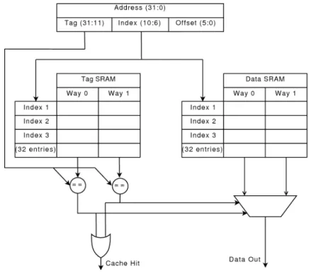
Figure 2.7 shows how cache lookup is performed in a set-associative cache. The address is split into three parts: the tag, the index and the offset. The index is used to index two SRAM arrays, the tag array and the data array. Since this is a two-way set associative cache, each index holds two tags. The tags from this array is compared to the tag portion of the address. If either tag matches, the data is in the cache (cache hit). The corresponding data line is then brought out of the data array by using a multiplexer. Since the cache lines are typically longer than the size of a word, the offset is used to further select what data from the cacheline to forward.
2.3.2
Cache Misses
There are three main reasons why data is not found in the cache. These are:
Definition 1 (Compulsory [47]):
Figure 2.7: Organization of a 4K two-way set associative cache with 64B cache lines.
into the cache. These are also called cold-start misses or first-reference misses. Definition 2 (Capacity [47]):
If the cache cannot contain all the blocks needed during the execution of a program, capacity misses (in addition to compulsory misses) will occur because of blocks being discarded and later retrieved.
Definition 3 (Conflict [47]):
If the block placement strategy is set associative or direct mapped, conflict misses (in addition to compulsory and capacity misses) will occur because a block may be discarded and later retrieved if too many blocks map to its set. These misses are also called collision misses or interference misses.
In a multiprocessor where data is shared between processors or cores, there is a
fourth type of cache miss called coherence miss. A coherence miss occurs due to
cache flushes to keep multiple caches coherent in a multiprocessor [31, 47, 140]. As an example, consider a two core CMP with separate private caches: Both cores reads the value of variable X from main memory. The value of X is then stored in both private caches. Core 1 then proceeds to modify X and stores the value. Now the value of X in main memory and core 2’s cache differs from the value in core 1’s
Block Address Target Information Valid Bit Figure 2.8: Conceptual MSHR entry
cache. These values are said to be invalid. An access by core 2 to X would then
cause a coherence miss.
2.3.3
Replacement Policies
After a cache miss new data is inserted into the cache. However, because of the cache’s limited capacity other data must be removed from the cache. There are
several possible replacement policies such as: Least Recently Used (LRU),First In,
First Out (FIFO) and random [128]. The most common replacement policy for general purpose processors is LRU, where the least recently accessed cache block is removed.
With the increased interest in CMPs andNon-Uniform Cache Architecture (NUCA)
there has been revived interest in cache replacement policies. Most cache misses are not performance-critical. In many cases, execution can continue regardless whether the load is a cache hit or miss. By reducing the number of isolated performance-critical cache misses, it is possible to increase the amount of MLP and perfor-mance [116]. When a cache block is evicted in NUCA, it can be moved to another cache. In that case, a policy for selecting a new cache is needed [32, 34].
2.3.4
Miss Status Holding Registers
Processors which can execute instructions Out-of-Order (OoO) has the potential
to issue multiple independent loads. To support this capability, caches need to be able to service more than a single access at a time. In particular, it must be able to handle multiple misses. To achieve this, it must keep an account of which misses are being serviced further down the memory hierarchy [80].
Miss Status Holding Registers (MSHRs)can be used for this purpose. A conceptual MSHR is shown in figure 2.8. A cache can sustain as many misses as there are MSHRs without blocking. Each MSHR holds the address that is being serviced and the target information for that miss. The target information is mainly what instruction caused the miss, and thus which instruction is waiting for the data and the destination register.
2.4
Prefetching
Prefetching is a technique to reduce the number of misses in a cache through predicting future memory references and fetching the corresponding data before it
is referenced by the CPU. It is especially effective for reducingcompulsory misses, as caches only retain previously referenced data. This can potentially speed up
execution significantly aspmissdecreases andLsystemdecreases. However, because
prefetching is a speculative technique some prefetched data will not be used, which
causes cache pollution and increased bandwidth usage. Agood prefetch is defined
as:
Definition 4 (Good prefetch [136]):
A prefetch is classified as good if the prefetched block is referenced by the application before it is replaced or bad otherwise.
A useful metric for dealing with prefetching isaccuracy. Accuracy is a metric for
how often the prefetcher’s prediction is correct:
Definition 5 (Accuracy [136]):
The accuracy of a given prefetch algorithm that yields G good prefetches and B bad prefetches is calculated as:
Accuracy= G
G+B (2.11)
It is not enough for a prefetcher to be accurate if the prefetches are issued too late. A prefetch must be issued sufficiently in advance so that it can be inserted into the
cache before it is referenced. This property is known astimeliness.
However, high accuracy and timeliness is not enough to ensure high performance. A significant portion of the program’s original cache misses must be eliminated to
increase performance. This is covered in thecoverage metric:
Definition 6 (Coverage [136]):
If a conventional cache has M misses without using any prefetch algorithm, the coverage of a given prefetch algorithm that yields G good prefetches and B bad prefetches is calculated as:
Coverage= G
M (2.12)
2.4.1
Sequential Prefetching
The simplest prefetching scheme is sequential prefetching [128]. Sequential pre-fetching simply fetches the next cache block when a cache block is accessed. Al-though this policy is simple, it is very effective because of sequential locality. Be-cause processors are much faster than main memory it is in practice necessary to fetch blocks further away than the next block such that the data is ready when the processor needs it. This is known as the prefetch distance:
Definition 7 (Prefetch distance [143]):
pre-fetches δ iterations before the data is referenced where δ is known as the prefetch distance and is expressed in units of loop iterations:
δ=
l s
(2.13) l is the average cache miss latency, measured in processor cycles and sis the esti-mated cycle time of the shortest possible execution path through one loop iteration.
Additionally, it might be beneficial to fetch multiple blocks at the same time. This parameter is the prefetch degree:
Definition 8 (Prefetch degree [143]):
It is possible to increase the number of blocks prefetched by any arbitrary number K. This number is known as the prefetching degree. As an example; a prefetching degree of 1 fetches 1 block from memory, while a prefetching degree of 3 fetches 3 blocks from memory.
These two parameters are often collectively referred to as the prefetcher’s
aggres-siveness. Increasing coverage usually comes at the expense of accuracy. A good prefetching scheme must thus balance the aggressiveness of the prefetcher to ensure a good trade-off between accuracy and coverage within the system’s limited off-chip bandwidth and cache capacity.
Tagged prefetching is a simple improvement over sequential prefetching [142]. In this scheme prefetched data is marked with a single bit in the cache. When this block is accessed the prefetcher knows that the previous prefetch for this data was successful and can initiate a request for the next line. This information can also be used to estimate prefetcher accuracy [135].
In most implementations, the prefetched data is inserted directly into the cache, which can cause useful data to be evicted. Another option is to use dedicated structures to hold the prefetched data such as stream buffers [71, 110]. A stream buffer is a structure that holds prefetched data which can be tailored to the type of prefetcher used. It is typically accessed in parallel with the main cache.
Another possibility is to predict which blocks in the cache is not needed any-more [82]. This information can be used to initiate prefetching for a new block to replace the old block, or it can be used to decide which block to replace when inserting new prefetches.
Additionally, in a CMP or multiprocessor system prefetching might cause invalida-tion of cache blocks in other cores [66]. For example, core 1 might hold an exclusive copy of a variable X, when core 2 decides to prefetch that block into it’s own cache. This forces core 1 to downgrade it’s copy of X to a shared state. However, if core 1 modifies X later, core 2’s copy must be invalidated which can decrease performance. A possible solution is to use instruction based sharing prediction to guide when to prefetch shared data, or simply avoid prefetching shared data [75].