An Intelligent Wireless Sensor Network Temperature
Acquisition System with an FPGA
Rachid Souissi1, Mohsen Ben-Ammar2 1
Computer Science Department, Higher Technological Institute of Sfax (ISET), Sfax, Tunisia 2
Electrical Engineering Department, National Engineering School of Sfax (ENIS) Machine Control and Power Grid Research Unit, CMERP, Sfax, Tunisia
Ema
Received September 27, 2013; revised October 27, 2013; accepted November 4, 2013
Copyright © 2014 Rachid Souissi, Mohsen Ben-Ammar. This is an open access article distributed under the Creative Commons At-tribution License, which permits unrestricted use, disAt-tribution, and reproduction in any medium, provided the original work is prop-erly cited. In accordance of the Creative Commons Attribution License all Copyrights © 2014 are reserved for SCIRP and the owner of the intellectual property Rachid Souissi, Mohsen Ben-Ammar. All Copyright © 2014 are guarded by law and by SCIRP as a guardian.
ABSTRACT
The use of FPGAs in the design of wireless sensor networks can improve the processing system performance so as to develop sensor nodes with powerful embedded processor. In fact, FPGA has a super-parallel processing capacity in data processing and its use and configuration is flexible. This allows intensive digital signal process-ing tasks like Fast Fourier Transforms to be implemented on the sensor node and this can even support intelli-gent applications and new security algorithms. This paper presents a wireless sensor network system that moni-tors and visualizes periodically the environment temperature. The proposed system consists of a base station node based on an FPGA DE2-70 and five sensor nodes having the architecture of the System-on-Chip CC2430.
KEYWORDS
Wireless Sensor Network; ZigBee; System-on-Chip CC2430; FPGA DE2-70
1. Introduction
The use of wireless sensor networks (WSNs) has risen in last years. In fact, several industrials, researchers and en-gineers work on this new technology both in the civilian and military sectors that require the use of many nodes, even hundreds or thousands. That is why more applica-tions have been developed in order to solve several prob-lems in data acquisition and environment control. More-over, these nodes must be capable of sensing, processing and communicating physical parameters like temperature and pressure through the global wireless network. This paper focuses on the designofa WSN to acquire the tem-perature from some autonomous nodes. It introduces the use of the FPGA DE2-70 in this application field. The use of the FPGA DE2-70 in WSN can improve the proc-essing system performance so as to develop powerful embedded processor. This paper highlights the different techniques, methods and protocols that can be used in this wireless sensor network technology. The developed system permits monitoring the environment temperature.
The organization of this paper is as follows; In Section 2, we will present some works dealing with sensor nodes mainly based on an FPGA, otherwise Section 3 deals with the IEEE 802.15.4 standard that defines the physical layer in all ZigBee devices; this standard is used by the sensor nodes to communicate with each other. Section 4 is devoted to the system hardware architecture; it exposes the main components of the system. The software archi-tecture is exposed in Section 5. The application descrip-tion is presented in Secdescrip-tion 6. Finally, a conclusion is given to the whole work.
2. Related Work
assumes that an input is detected and thus the car is en-tered into the parking lot. As the car leaves the lot, it is detected by the IR sensors. The IR sensors provide the pulse to the FPGA which assumes that an input is de-tected and thus the car is exited out of the parking lot.
The project [2] has been carried out to develop a novel FPGA-based photosynthesis smart sensor. The smart sensor is capable of acquiring and fusing the primary sensor signals to measure temperature, relative humidity, solar radiation, CO2, air pressure and air flow. This per-mits the estimation of carbon balance, integrative and derivative variables from net photosynthesis in real time due to the FPGA processing capabilities. To accomplish this, high performance computational capabilities are required. These days, Field Programmable Gate Arrays (FPGAs) are devices that are being employed in applica-tions where high demand computational resources are necessary (Contreras-Medina et al., 2012). Due to the demands for high computation required in this research the use of FPGA-based smart sensor with capabilities of acquiring the primary sensor readings, memory man-agement, signal processing, photosynthesis calculation, wireless communication management and in situ real time photosynthesis signal visualization in a color LCD screen is proposed.
In this work [3], we have developed a modular node. So, both digital and analogue type sensors are being con-sidered. The signals that they produce are conditioned for interfacing to the processing and communications mod-ules. For processing there is a field programmable gate array (FPGA) module. This allows intensive digital sig-nal processing (DSP) tasks such as moving average fil-ters, Fast Fourier Transforms (FFTs) to be implemented on the sensor node and this can even support intelligent applications.The FPGA module was included as this pro-vides a reconfigurable processing solution in which in-tensive DSP Tasks or in which intelligent functionality can be implemented.
In [4], Wei et al. presented a sensor node based on SoC. Such SoC is based on the OpenRisc1200 processor and executes the µ/OS II RTOS and Wishbone bus. The SoC consists of three main components: an acquisition unit that is fed from a digital thermometer coupled to the FPGA, the OpenRisc firmware that processes the tem-perature and a logic block that interfaces a ZigBee trans-ceiver based on RS-232 (SHUNCOM SZ05-STD). The utilized FPGA is an Altera Cyclone II (EP2C70). The system consumes 221 mW. Nevertheless, given that the FPGA only interfaces several components (digital ther-mometer and ZigBee transmitter), it seems to be an over-kill, since its inner embedded resources are not used and the same task can be performed using a low-power mi-crocontroller.
3. The Communication Stack
The proposed system uses the IEEE 802.15.4 standard [5] as the communication protocol. The IEEE 802.15.4 stan-dard defines the characteristics of the physical and MAC layers for Low-Rate Wireless Personal Area Networks (LR-WPAN) including wireless sensor networks (WSNs). IEEE 802.15.4 focuses mainly on low-cost, low-power communication between devices and therefore it presents a low transfer rate with a maximum of 250 kbits/s.
3.1. Physical (PHY) Layer
The IEEE 802.15.4 standard defines the physical layer (PHY) in all ZigBee devices. The PHY is responsible for data transmission and reception by using a defined radio channel and specific modulation and spreading technique [6]. The IEEE 802.15.4 standard specifies two physical layers that represent three operational frequency bands. These three bands include: 868 MHz (used in Europe), 915 MHz (used in America), and 2.4 GHz (used world-wide) [7]. The 868 and 915 MHz bands are in one PHY using the Binary Phase Shift Keying (BPSK) for modula-tion, while the 2.4 GHz band is in the second PHY and employs Offset Quadrature Phase Shift Keying (O-QPSK) for modulation. There is a single channel between 868 and 868.8 MHz, 10 channels between 902 and 928 MHz, and 16 Channels between 2.4 and 2.4835 GHz, all using the Direct Sequence Spread Spectrum (DSSS) access mode[6].
3.2. Medium Access Control (MAC) Layer
In addition to the physical layer, the IEEE 802.15.4 stan-dard defines the medium access control layer for all Zig-Bee devices. The MAC layer protocol serves as the in-terface between the PHY and the higher layer protocols. The functions of the MAC include synchronization, frame validation, acknowledged frame delivery, associa-tion, and disassociation [5,8].
The MAC layer defines two types of devices; Full Function Device (FFD) and Reduced Function Device (RFD).
channel by employing some methods like the Carrier Sense Multiple Access with Collision Avoidance (CSMA/CA) mechanism. CSMA/CA is a network con-tention protocol that listens to the network before send-ing, in order to avoid collision [8].
3.3. ZigBee Layers
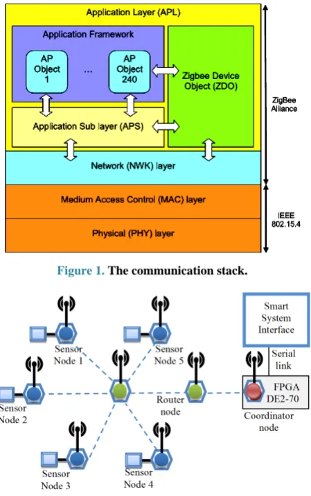
Based on the IEEE 802.15.4, the ZigBee standard [9] defines the higher layer namely; the network layer and the application layer (Figure 1).
The network layer is responsible for joining/leaving a network, security, routing, discovering 1-hop neighbors and storing neighbor information. The ZigBee network layer supports three topologies; the star topology where end devices (RFD) are attached to a central point playing the role of PAN coordinator (FFD), the tree topology where end devices can be attached also to FFD nodes with routing capabilities playing the role of ZigBee routers in a hierarchical manner (with parent-child rela-tionship), the mesh topology where ZigBee routers can be fully connected.
As shown in Figure 1, the application layer includes the Application Framework, the ZigBee Device Objects (ZDO), and the Application Sub Layer (APS). The Ap-plication Framework can have up to 240 ApAp-plication Ob-jects (APOs), that is, user defined application modules which are part of a ZigBee application [6]. The ZDO defines the role of the device, initiates and responds to binding requests and establishes a secure relationship between devices. The APS offers an interface to data and security services to the APO sand ZDO.
4. Hardware Architecture
As shown in Figure 2, our system consists of three types of entities. An end device is a sensor nodes composed by one System-on-Chip (CC2430) and is responsible for sensing environment parameters (such as temperature) and then sending the sensed data to the base station. The base station contains a System-on-Chip (CC2430) and is connected to an FPGA DE2-70 through its expansion header. The base station is responsible for collecting data from end devices. After that, the FPGA DE2-70 reads this information then sends it joined with the address of the appropriate node to the personal computer through one serial link. The PC is responsible for visualizing the received information for further analysis and interpreta-tion [10].
4.1. The FPGA DE2-70
[image:3.595.313.538.84.442.2]The Altera FPGA is widely used as the programmable device to support the Design and Reuse (D & R). This is even more convenient with the development of System
Figure 1. The communication stack.
Figure 2. System architecture.
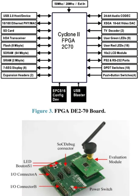
on Programmable Chip (SOPC) where Altera is leading the industry with its FPGA chips and the Quartus Appli-cation tools. The Altera Nios is 32-bit softcore RISC processor that is optimized for Altera Field Programma-ble Gate Array (FPGA) devices. It is a powerful embed-ded processor and is mainly used to control reconfigur-able circuits running on the Altera FPGA. A schema of the DE2-70 board is shown in Figure 3. It depicts the layout of the board and indicates the location of the con-nectors and key components.
4.2. BB—Battery Board
Figure 3. FPGA DE2-70 Board.
Figure 4. System-on-Chip Battery Board with CC2430EM.
SOC network [11]. The photograph of the component is shown in the Figure 4. On this Battery Board, we can find the Evaluation Module, which contains the mini-mum Components for a RF part to function.
4.3. System-on-Chip CC2430
The CC2430 comes in three different versions: CC2430- F32/64/128, with 32/64/128 KB of flash memory respec-tively. The CC2430 is a true System-on-Chip (SoC) solu-tion specifically tailored for IEEE 802.15.4 and Zig-Bee™ applications. It enables ZigZig-Bee™ nodes to be built with very low total bill-of material costs.
The CC2430 combines the excellent performance of the leading CC2420 RF transceiver with an industry- standard enhanced 8051 MCU, 32/64/128 KB flash memory, 8 KB RAM and many other powerful features. Combined with the industry leading ZigBee™ protocol stack (Z-Stack), the CC2430 provides the market’s most competitive ZigBee™ solution.
The CC2430 is highly suited for systems where ultra- low power consumption is required. This is ensured by various operating modes. Short transition times between operating modes further ensure low power consumption.
4.4. 8051 CPU
The CC2430 includes an 8-bit CPU core which is an en-hanced version of the industry standard 8051 core. The enhanced 8051 core uses the standard 8051 instruction set. Instructions execute faster than the standard 8051 due to the following:
• One clock per instruction cycle is used as opposed to 12 clocks per instruction cycle in the standard 8051; • Wasted bus states are eliminated. Since an instruction
cycle is aligned with memory fetch when possible, most of the single byte instructions are performed in a single clock cycle.
5. Software Architecture
The design of the software in this package is based on the layered architecture as depicted in Figure 5.
Application layer: This Software package contains se- veral applications examples with access to Basic RF and HAL (Hardware Abstraction Layer) [12].
Basic RF: This layer offers a simple protocol for trans-mission and reception on two-way RF link.
Hardware Abstraction Layer: Contains functionality for access to the radio and on-board peripherals modules like LCD, UART, joysticks, buttons, and timers [5].
5.1. Basic RF
The Basic RF layer offers a simple protocol for transmis-sion and reception on a two-way RF link. The Basic RF protocol offers the service for packet transmission and reception. It also offers secure communication by use of CCM-64 authentication and encryption/decryption of packets. The security features of Basic RF can be com-piled in by defining the compile switch SECURITY_ CCM in the project file. The compile time inclusion of security features is done to save code space for the ap-plications where security features are not needed [5]. The protocol uses IEEE 802.15.4 MAC compliant data and acknowledgment packets. However, it does not offer a full MAC layer, only a simple data link layer for com-munication between two nodes. Basic RF contains only a small subset of the 802.15.4 standard:
[image:4.595.347.498.634.719.2]• Association, scanning or beacons are not imple-mented;
• No defined coordinator/device roles (peer-to-peer, all nodes are equal);
• No packet retransmission. This must be taken care of by the layer above Basic RF.
5.2. Basic RF Instructions
5.2.1. Startup
1) Make sure that the board peripherals and radio in-terface is initialized i.e. halBoardInit() must have been called first.
2) Create a basicRfCfg_t structure, and initialize its members. If the security features of Basic RF are used, the higher layer is responsible for allocating and assign-ing the 16 bytes key.
3) Call basicRfInit() to initialize the packet protocol.
5.2.2. Transmission
1) Create a buffer with the payload to send. Maximum payload size for Basic RF is 103 Bytes.
2) Call basicRfSendPacket(). Check the return value.
5.2.3. Reception
1) Perform polling by calling basicRfPacketIsReady() to check if a new packet is ready to be received by the higher layer.
2) Call basicRfReceive() to receive the packet by higher layer. The caller is responsible for allocating a buffer large enough for the packet and 2 Bytes buffer space for the RSSI value [13].
5.3. IAR Embedded Workbench® for 8051
IAR Embedded Workbench is a set of highly sophisti-cated and easy-to-use development tools for embedded applications. It integrates the IAR C/C++ Compiler™, assembler, linker, librarian, text editor, project manager, and C-SPY® Debugger in an integrated development environment (IDE). With its built-in chip-specific code optimizer, IAR Embedded Workbench generates very efficient and reliable FLASH/PROMable code for the 8051 microcontroller. In addition to this solid technology, IAR Systems also provides professional worldwide tech-nical support. So, we have used this environment to write then download program of each node inside his FLASH EPROM.
6. Results and Discussion
Our application is composed by two modules “Node()” and “FPGADE270()”. The “Node()” moduleis executed on the end devicenodes, while the “FPGADE270()” module is executed on the base stationnode CC2430(bs) linked to the FPGA DE2-70. The module “Node()” will read the temperature of each node and send the
appropri-ate value joined with the address of the node to the main node CC2430(bs) linked to the FPGA DE2-70. When the information is received, it will be sent to the Personal Computer through the serial port where it will be visual-ised.
6.1. The “Node” Module
In this module we have implemented a function that per-mits to read the temperature. This function will read the temperature of the node, then return the appropriate value to the parent module executed on the node. In fact, in order to get the temperature we have used the predefined functionadcSampleSingle(ADC_REF_1_25_V,ADC_12_ BIT,ADC_TEMP_SENS).
#include <adc.h> #ifndef _HAL_TEMP_H #define _HAL_TEMP_H
#define ADC_REF_1_25_V0x00// Internal 1.25V reference
#define ADC_12_BIT 0x30 // 512 decimation rate
#define ADC_TEMP_SENS 0x0E// on-chip temperature sen-sor
#define CONST 0.61065 // (1250 / 2047)
#define OFFSET_DATASHEET 743 #define
OFFSET_MEASURED_AT_25_DEGREES_CELCIUS 29.75
#define OFFSET (OFFSET_DATASHEET + OFFSET_MEASURED_AT_25_DEGREES_CELCIUS)
// 779.75
#define TEMP_COEFF 2.45 unsigned char getTemp(void) {
unsignedintadcValue; floatoutputVoltage;
ad-cValue=adcSampleSingle(ADC_REF_1_25_V,AD C_12_BIT,ADC_TEMP_SENS);
adcValue>>= 4;
outputVoltage = adcValue * CONST; return ((outputVoltage - OFFSET) / TEMP_COEFF); }
When the temperature is acquired, the node will send it to the main node or to his neighbour in general, so we have developed the following module in order to do this RF transmission. So, in the following module we will call the function getTemp() to get the temperature of each node.
#define PAN_ID 0x2007 #define CLIENT_ADDR 0x2524 #define SERVEUR_ADDR 0xBEEF #define APP_PAYLOAD_LENGTH 3
#define a 0 #define b 1 static void Node() {
pTxData[a] = CLIENT_ADDR;
basicRfConfig.myAddr = SERVEUR_ADDR; if(basicRfInit(&basicRfConfig)==FAILED) { HAL_ASSERT(FALSE); }
while (TRUE) { halLedToggle(1);
pTxData[b] = getTemp();
basicRfSend-Packet(SERVEUR_ADDR,pTxData,APP_PAYLOAD_ LENGTH);
halIntOff();
halMcuSetLowPowerMode(HAL_MCU_LPM_3); halIntOn();
} }
6.2. The FPGADE270 Module
#define APP_PAYLOAD_LENGTH 3 #define a 0
#define b 1
static uint8 pRxData[APP_PAYLOAD_LENGTH]; static void FPGADE270()
{ while (TRUE) {
while(!basicRfPacketIsReady());
basicRfReceive(pRxData, APP_PAYLOAD_LENGTH, NULL);
long temp=pRxData[b]; P0DIR=0xFF;
P0=pRxData[a]; halMcuWaitMs(100); P0=pRxData[b]; }}
In this module, we receive the appropriate value of the temperature of the node. In fact, to reach this goal we have used the predefined function basicRfReceive(pRx Data, APP_PAYLOAD_LENGTH, NULL) to read the information send by each node. This information is stored in the vector pRxData. So, the temperature is stored in pRxData[b] while the address of the node is in the pRxData[a].
6.3. Monitoring Interface
When the temperature is received by the FPGADE270 node it will be send later through the serial port to the personal computer where it will be visualised by one interface developed with Matlab Version R2012a as de-picted in the following figures. So, the Figure 6(a) illus-trates the results taken in hot period like June. Otherwise, in the Figure 6(b) we can see the results related to cold period like December month.
(a)
(b)
Figure 6. (a) Acquisition results in June the 30th 2013; (b) Acquisition results in December the 1st 2013.
In this interface we can see an important increase of temperature values send by each node and other informa-tion like the time of each received informainforma-tion.
7. Conclusions
The development of wireless sensor network reveals new challenges to engineers in several fields. In this context, the development of systems based on wireless sensor networks becomes a necessity. Therefore, actually we are obliged to develop some systems based on this new technology to solve several problems in data acquisition and control in different environments.
Our system includes two aspects: hardware and soft-ware. The hardware is composed of one base node CC2430(bs) connected to the FPGA DE2-70 and five nodes CC2430(1..5). Each component contains a System- on-Chip CC2430 that contains the processor which exe-cutes the necessary program on each node. The applica-tion permits monitoring temperature of the environment. The future work is to develop a synchronisation algo-rithm to coordinate between transmissions of each node. Moreover, the information received by the WSN will be visualised through the internet network in order to bene-fit from the distant control and monitoring.
[image:6.595.309.538.83.367.2]can use more than five nodes, for example twenty nodes and the distance between two nodes is twenty meter, so each node can send his information to his neighbour node until the final destination or the main node CC2430(bs). So, the role of each node is to acquire the temperature from his location, receive and send information to the next node until we reach the last destination. By this way, the WSN will be installed in large area, in order to su-pervise it.
REFERENCES
[1] R. Khan, Y. Ali Shah, Z. Khan, K. A. Muhammad and A. M. Amjad Ali, “Intelligent Car Parking Management Sys- tem on FPGA,” IJCSI International Journal of Computer Science Issues, Vol. 10, No. 1, 2013, pp. 171-173.
[2] J. R. Millan-Almaraz, I. Torres-Pacheco, C. Duarte-Gal- van, R. G. Guevara-Gonzalez, L. Miguel Contreras-Medi- na, R. de Jesus Romero-Troncoso and J. R. Rivera-Guil- len, “FPGA-Based Wireless Smart Sensor for Real-Time Photosynthesis,” Computers and Electronics in Agricul-ture, Vol. 93, 2013, pp. 58-69.
[3] S. J. Bellis, K. Delaney, B. O’Flynn, J. Barton, K. M. Razeeb and C. O’Mathuna, “Development of Field Pro- grammable Modular Wireless Sensor Network Nodes for Ambient Systems,” University College Cork, Cork, 2005.
[4] J. Wei, L. Wang, F. Wu, Y. Chen and L. Ju, “Design and Implementation of Wireless Sensor Node Based on Open Core,” Proceedings of the IEEE Youth Conference on In-formation, Computing and Telecommunication, Beijing, China, 20-21 September 2009, pp. 102-105.
[5] Institute of Electrical and Electronics Engineers, Inc., IEEE Std.802.15.4-2003, “Wireless Medium Access Control (MAC) and Physical Layer (PHY) Specifications for Low Rate Wireless Personal Area Networks (LR- WPANs),” IEEE Press, New York, 2003.
[6] P. Baronti, P. Pillai, V. WC. Chook, S. Chessa, A. Gotta and Y. Fun Hu, “Wireless Sensor Networks: A Survey on the State of the Art and the 802.15.4 and ZigBee Stan- dards,” Computer Communications, Vol. 30, No. 7, 2007, pp. 1655-1695.
[7] K. Scott, “Design and Performance of IEEE 802.15.4. Compliant MSE Receivers,” Asilomar Conference on Signals, Systems and Computers, Vol. 2, November 2004, pp. 2051-2055.
[8] G. Ding, B. Bhargava, Z. Sahinoglu and P. Zhang, “Reli-able Broadcast in ZigBee Networks,” IEEE SECON Pro-ceedings, 2005, pp. 510-520.
[9] ZigBee Alliance, “ZigBee Specifications,” Version 1.0, 2005.
[10] CC2430 Software Examples Users Guide TEXAS IN- STRUMENTS.
[11] Chipcon Products from Texas Instruments, CC2431DK Development Kit User Manual Rev. 1.5.
[12] Y. E. Krasteva, J. Portilla, M. Carnicer, E. de la Torre and T. Riesgo, “Remote HW-SW Reconfigurable Wireless Sensor Nodes,” Industrial Electronics, 2008.