N A N O E X P R E S S
Open Access
Colloidal crystals by electrospraying polystyrene
nanofluids
Arnau Coll, Sandra Bermejo
*, David Hernández and Luis Castañer
Abstract
This work introduces the electrospray technique as a suitable option to fabricate large-scale colloidal
nanostructures, including colloidal crystals, in just a few minutes. It is shown that by changing the deposition conditions, different metamaterials can be fabricated: from scattered monolayers of polystyrene nanospheres to self-assembled three-dimensional ordered nanolayers having colloidal crystal properties. The electrospray technique overcomes the main problems encountered by top-down fabrication approaches, largely simplifying the
experimental setup. Polystyrene nanospheres, with 360-nm diameter, were typically electrosprayed using off-the-shelf nanofluids. Several parameters of the setup and deposition conditions were explored, namely the distance between electrodes, nanofluid conductivity, applied voltage, and deposition rate. Layers thicker than 20μm and area of 1 cm2were typically produced, showing several domains of tens of microns wide with dislocations in between, but no cracks. The applied voltage was in the range of 10 kV, and the conductivity of the colloidal solution was in the range of 3 to 4 mS. Besides the morphology of the layers, the quality was also assessed by means of optical reflectance measurements showing an 80% reflectivity peak in the vicinity of 950-nm wavelength.
Keywords:Electrospray, Nanospheres, Colloidal crystal, Multilayer, Metamaterial
Background
Self-assembly is a technological process resulting in an ordered structure of individual units without direct human intervention. Most often, this is the simplest technique to produce nanoscale structures, and this is the main reason of the recent wide interest, as revealed by comprehensive compilations. Some reviews [1-4] ex-haustively describe the different existing technologies, mainly based on electrophoretic forces [5], capillary forces [6,7], dip coating [8,9], and ink-jet printing [10], among others.
Top-down approaches, such as lithography or ion sput-tering, have smaller chances to be able to produce large-scale low cost materials than bottom-up wet methods, despite the limitations of techniques such as spinning or sedimentation. Mono- and multilayers of nanospheres have a huge number of promising electrical and optical applications [11-14]; some benefiting from the high surface-to-volume ratio to, for example, foster a new
generation of ultrafast bulk battery electrodes [15], scaffolds of macroporous materials [16,17], while others benefit from the dimension of the periodicity of three-dimensional (3D) structures making them suitable for photonic [18-20] or terahertz applications [21].
The technique used in this work is known as electro-spray. It consists of producing a fine aerosol by disper-sion of a liquid by application of a high electric field between an emitter, usually a thin needle, and a flat elec-trode. Above a given voltage threshold, a Taylor cone develops [22] and the liquid tip becomes unstable break-ing into small droplets. The main application of electro-spray is found in the ion source of mass spectrometers, although it has also been recently used as a nanoparticle deposition method [23-25], polymer thin film deposition [26], or to create photonic balls [27]. To our knowledge, electrospraying of nanofluids or colloidal solutions of nanometer-size spheres to produce full 3D self-assembled crystals has not been reported so far. A very comphensive work on state-of-the-art colloidal crystals has re-cently been published [1] where a few indicators of the crystal quality produced by the various techniques are * Correspondence:[email protected]
MNT, Electronic Engineering Department, Universitat Politècnica de Catalunya, Jordi Girona 1-3, Barcelona 08034, Spain
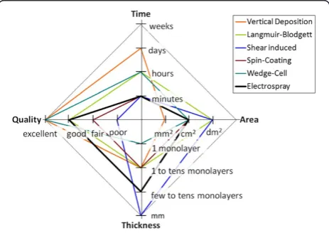
summarized and compared, namely the thickness, area, deposition time, and optical quality.
We have drawn in Figure 1 a radial plot of selected in-formation from Table one in [1] for some of the depos-ition techniques reported there. We have not included the indicators concerning four techniques, namely motor-drawing, sedimentation, cell confinement, and air-water interface due to the poor results compared to the rest.
As can be seen in Figure 1, the most successful techni-ques exhibit good to poor optical quality, but deposition times are long and the crystal size is in the range of square millimeter of area. It can be seen that the only technique being able to provide wafer-size colloidal crys-tals (tens of square centimeter in area) in some minutes is the spin-coating technique. It can be seen from this plot that the combination of large area, tens of mono-layers of thickness, range of minutes to fabricate, good or excellent optical quality of the crystals, and 3D order is difficult to achieve in most of the techniques. In Figure 1, we have highlighted the results that we have achieved with the technique we are describing in this paper: the electrospray. Using this technique, we were able to deposit up to tens of monolayers, in a few min-utes, in square centimeter size, with 3D order, and with good quality. These remarkable results, which are described in the sections below, compare quite well with the other state-of-the-art techniques reported in Figure 1. Thus, we can claim to have achieved a good compromise between large area and low deposition time, achieving good quality of the colloidal nanostructures.
In this work, the deposition conditions, such as flow rate, solution concentration, electrical potential, and dis-tance between electrodes, are examined to find the
optimal deposition conditions to create 3D self-assembly crystals. In the electrospraying deposition of particles on a substrate, several forces and physical phenomena are involved. In the short range, electrostatic forces are im-portant, in addition to surface tension and capillarity, to explain particle adhesion to surfaces and particle chain, formation, or self-assembly. Coulombic and multipolar dielectrophoretic forces contribute to the total force act-ing on the particles, thereby affectact-ing the adhesion regimes. The sign and magnitude of the dielectrophore-tic component depends on the Claussius-Mossotty factor [28], which depends on the values of the permittivity of the particle and of the medium. In this work, we have observed a set of experimental conditions leading to net attractive forces between particles, so they aggregate in the three dimensions of the layer growth. Scanning elec-tron microscope (SEM) images and optical measure-ments are also shown to demonstrate the quality of the fabricated colloidal crystals.
Methods
The electrospray setup consisted of an infusion pump from B. Braun SA (Melsungen, Germany), an OMNIFIX (Braun) 5-ml syringe, a Hamilton needle (600-μm outer
and 130-μm inner diameter; Hamilton, Bonaduz, GR,
Switzerland), and an Ultravolt high-voltage bipolar source, −15 kV to +15 kV (Ultravolt, Ronkonkoma, NY, USA). The deposition area was placed inside a glove box with controlled N2atmosphere. Figure 2 shows
schemat-ically the experimental setup.
[image:2.595.58.290.513.677.2]In this work, silicon and glass substrates were both used, and they were covered either with aluminum or ITO patterned layers typically 120-nm thick. ITO elec-trodes allow optical observation as it has good optical transmission [29]. Polystyrene nanospheres, 360 nm in diameter, were electrosprayed targeting these patterned electrode areas. The main parameters that were explored in the experiments were the value of applied voltage, the
[image:2.595.304.540.562.693.2]Figure 1Radial plot of quality indicators for some of the most relevant colloidal crystal fabrication techniques.Deposition time, area, thickness, and quality of the photonic crystal are compared. The technology introduced in this work is the electrospray, in solid black.
distance from the needle to the substrate, the solution concentration, the solution conductivity, and the depos-ition time.
The first efforts were devoted to finding suitable ex-perimental conditions to get a stable Taylor cone at the tip of the needle. This involved changing the distance from the needle to the substrate and changing the bias conditions. We found that a Taylor cone was created when the distance was typically between 10 to 15 cm and the applied voltage difference was between 7,500 and 14,000 V. Differences in the deposition results were also found when the substrate was grounded rather than negatively biased. Our best results were obtained when
−1,000 V was applied to the substrate and +9,000 V was applied to the needle.
[image:3.595.57.537.112.296.2]Once the conditions for Taylor cone creation were found, the effects of the solution pumping rate, solution concentration, and solution conductivity were explored. No effects on the order of the deposited layers were found by just changing the solution concentration. Our best results were found for 350-μS solution conductivity and 2.2-ml/h pumping rate, provided the voltage condi-tions were as described above, +9,000 V at the needle and −1,000 V at the substrate. For these conditions, the deposited film was composed of tens of ordered layers. Additionally, increasing the conductivity to the range of Table 1 List of the most relevant experimental conditions in the electrospray deposition of 360-nm polystyrene nanospheres
Distance (cm)
Needle's voltage (V)
Sample's voltage (V)
Deposition rate (ml/h)
Conductivity (μS)
Dissolution Qualitative assessment
10 10,000 −2,350 0.41 8.35 50:50 isopropanol/water nanopolystyrene
Few dispersed nanospheres
10 7,500 −2,500 0.74 8.35 50:50 isopropanol/water
nanopolystyrene
Few dispersed nanospheres
10 14,000 0 1.3 350 Water nanopolystyrene Few dispersed nanospheres
14 14,000 0 0.3 350 Water nanopolystyrene Few dispersed nanospheres
14,5 11,570 0 2 350 Water nanopolystyrene Lots of dispersed
nanospheres
14,5 9,000 −1,000 0.2 350 Water nanopolystyrene Few dispersed nanospheres
14,5 9,000 −1,000 0.2 350 Water nanopolystyrene Few dispersed nanospheres
14 9,000 −1,000 0.6 4,100 50:50 water nanopolystyrene/distilled water + 1.5% formic acid
Semi-covered layer of scattered nanospheres
14 9,000 −1,000 2.2 350 Water nanopolystyrene Tens of 3D ordered layers
In all the processes, the humidity was monitored during deposition and typically was 20%.
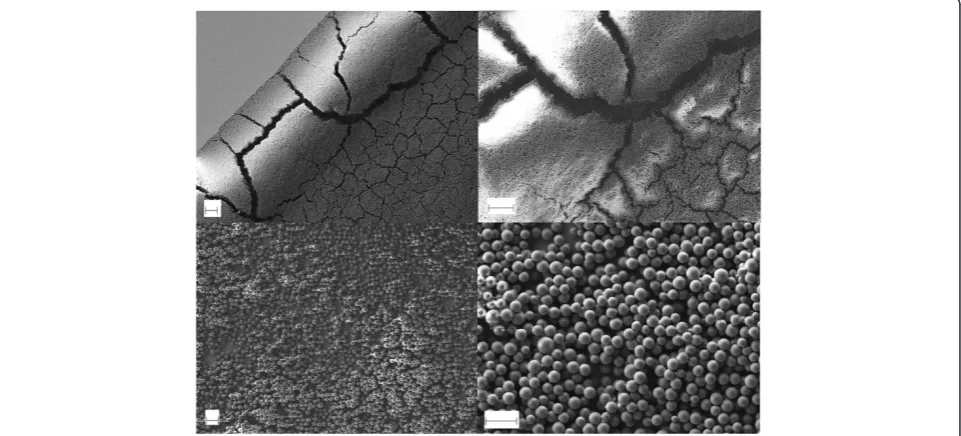
[image:3.595.58.539.487.705.2]Figure 4Semi-covered layer of scattered nanospheres.SEM pictures showing a monolayer of 360-nm polystyrene nanospheres deposited under the conditions shown in the eighth row of Table 1. The semi-covered monolayer follows the patterned contact, a squared electrode in the center of the left image and a path for electrical conduction at the top. Scale bar is 200μm.
[image:4.595.55.540.344.706.2]4 mS by adding formic acid to the solution and decreas-ing the concentration of nanospheres tend to produce smaller droplets and layers of scattered nanospheres.
In our experience, to get ordered layers, some liquid of the aerosol is required at the surface of the substrate and, once the conditions to get a Taylor cone are satis-fied, only the pumping rate and the solution conductivity seem to play an important role and not the solution centration. A summary of some of the experimental con-ditions we have explored is shown in Table 1. Only the conditions leading to a Taylor cone formation are shown.
Results and discussion
Following the experiments shown in Table 1, in this sec-tion, SEM observations and optical measurements are shown. When the conditions for a Taylor cone formation are not met, drops fall on top of the substrate, and when they dry, no significant order is observed in the nano-sphere aggregation, as can be seen in Figure 3. The results obtained using the experimental conditions described
in Table 1 can be summarized into two main groups: (1) some order is reached in semi-covered areas (Figure 4), and (2) complete 3D order is achieved in the whole area (Figures 5, 6, 7, 8).
Figure 4 shows the SEM pictures of a layer deposited using the conditions reported in the eighth row of Table 1. As can be seen, the layer involves scattered nanospheres with no 3D order. Metal areas are pat-terned on the surface of the substrate to define electrode areas that, when high voltage is applied, act as collection points where the nanospheres are self-assembled.
A number of observations were made on the films deposited for the conditions in the last row of Table 1. We first took optical pictures of the front surface when illuminated by a warm white LED (3,000 to 3,500 K) light at different incidence angles. This is shown in Figure 5, where the iridescence of the material can be seen.
[image:5.595.59.539.89.285.2] [image:5.595.57.538.600.720.2]Surface and in-depth SEM observations have also been performed, and the results are shown in Figure 6. Figure 6a shows a side view of the deposited layer after Figure 6SEM pictures of 360-nm-diameter polystyrene nanosphere layers.(a) Cut surface showing [1 0 0] and [1 1 1] ordered facets, (b) close view of the perpendicular cut, (c) close view of the [1 1 1] face, and (d) top view of the [1 0 0] (top) and [1 1 0] order (bottom).
we performed a focused ion beam (FIB) milling. A closer view of the orthogonal corner in Figure 6a is shown in Figure 6b, where the (100) order of the top surface and of the two orthogonal planes etched by the FIB can be seen. A closer view of the edge of the top surface and of the inclined plane can be seen in Figure 6c, where the (100) and (111) orders are clearly seen. This is further seen in Figure 6d, where the (110) and (100) faces are also shown. The results shown in Figure 6 clearly dem-onstrate that the order of the self-assembly extends tens of layers in depth, reaching thicknesses of more than 20μm, although we have not found a fundamental rea-son to prevent the formation of thicker layers with simi-lar order, provided the deposition time is increased.
Polystyrene nanospheres of 760-nm diameter have also been deposited, reaching 3D ordered structures as well. Figure 7 shows 760-nm-diameter polystyrene nano-spheres deposited under the same conditions shown in Figure 6: +9 kV needle bias and −1 kV substrate bias. The dissolution was an off-the-shelf distilled water solu-tion of 760-nm polystyrene nanospheres, the pumping rate was 2.2 ml/h, and the deposition time was 10 min.
A macroscopic observation of the surface of the deposited layers demonstrates the existence of several domains of tens of microns wide. Inside every domain, the same order is kept, and dislocations can be seen in the frontiers between domains, as shown in Figure 8. Less than 0.5% defects in average are found inside each domain.
The experimental arrangement involves a very high voltage between a sharp electrode above a larger and flat electrode. It is well known that this arrangement creates an electric field distribution involving large gradients. This is the origin of the dielectrophoretic force that the nanospheres are subjected to. From our observations, we have first witnessed that below a certain value of ap-plied voltage for a given electrodes distance, no 3D ordered layer is deposited, and this may be consistent with the threshold electric field value for Taylor cone formation and that postulated by Schwan and Sher [30] for chain formation, thereby indicating that neither con-ditions for aerosol formation nor particle aggregation
are satisfied. We have also seen that our best results are obtained when a moderate value of the solution con-ductivity is used and when some liquid from the aerosol reaches the substrate. This may be consistent with the value and sign of the Clausius-Mossotty factor to create predominantly attractive forces between particles that tend to aggregate. Moreover, we have observed that when the conductivity of the solution is much increased, the layer deposited consisted of predominantly scattered nanospheres, which is consistent with dominant repul-sive forces between them as a result of particle dipole interaction [31] and the dielectrophoretic force from the main field created by the needle tip and the bottom electrode.
[image:6.595.57.539.89.178.2] [image:6.595.307.540.490.704.2]The detailed explanation on how the dielectrophoretic force on the particles stimulates the orderly deposition of the spheres requires further work as particle align-ment and enhancealign-ment of net electrostatic adhesion force have been described for xerographic applications [31]. Our work opens the way to investigate other electrode Figure 8Top view of large domains of polystyrene nanosphere layer.SEM pictures of a colloidal crystal of 360-nm-diameter polystyrene nanospheres electrosprayed onto a silicon substrate deposited under the conditions described for Figure 6: (a) surface of the crystal showing the several domains and (b) a closer view of the dislocation between domains. Scale bars are 1μm.
geometries and spatial and temporal dependence of the electric field to further improve deposition.
To complete the study on ordering quality, we have measured the optical reflectance of the crystals by in-frared spectroscopy (see Figure 9). Spheres pack on an ordered combination of face-centered cube (FCC) and hexagonal close-packed (HCP) lattice, as observed from SEM images (Figure 6). The photonic band structure of an FCC lattice of dielectric nanospheres does not allow the opening of a full optical bandgap, neither HCP ar-rangement, but only of a pseudo optical bandgap along the L direction of the Brillouin zone [32]. As expected, there is a reflectivity increase in the spectral region 929 to 980 nm peaking close to 950 nm, with a maximum value of 75.1%. This result is consistent with theoretical calculations carried out using the plane wave expansion method, which predicts a relative stop band in the nor-mal direction of the crystal.
The optical measurements were made with a Shimadzu (Kyoto, Japan) UV3600 UV–VIS-NIR spectrophotometer and an ISR-3100 integrating sphere attachment of 3 mm × 12 mm beam area. All the reflectance measurements were made in the range of 700 to 1,200 nm. The measured sam-ple consists of an approximately 1-cm2colloidal crystal of 360-nm-diameter polystyrene nanospheres electrosprayed onto a glass substrate covered by a 100-nm-thick ITO layer.
Conclusions
We can conclude that a simple electrospray method is able to produce thick layers of tridimensional order from off-the-shelf colloidal solutions of nanospheres. Polystyrene nanospheres 360 and 780 nm in diameter were electrosprayed onto 1-cm2 metalized areas. Ex-perimental work was made to achieve 3D ordered nanostructures up to 20-μm thick in a few minutes, totally avoiding cracks. With the dimensions used in this work, it is shown that the deposited layers be-have as a photonic crystal exhibiting a stop band in the NIR, according to theoretical predictions, thereby demonstrating good quality of the deposited layers.
Competing interests
The authors declare that they have no competing interests.
Authors’contributions
AC and SB assembled the electrospray setup and deposited the layers. DH did the spectrometry measurements. LC suggested the use of electrospray for the deposition of colloidal crystals and wrote the paper together with AC and SB. All authors read and approved the final manuscript.
Acknowledgments
This work has been partially supported by the Spanish Ministry of Science and Innovation under projects AYA2011-29967-C05-04, TEC2010-18222 co-financed with FEDER funds and the Network of Excellence‘Nanophotonics for Energy’. SEM and optical measurements have been performed at CRNE. The authors thank Triffon Triffonov and Moises Garín for their helpful discussions.
Received: 4 December 2012 Accepted: 2 January 2013 Published: 12 January 2013
References
1. Galisteo-López J, Ibisate M, Sapienza R, Froufe-Pérez L, Blanco A, López C: Self-assembled photonic structures.Adv Mater2011,23:30.
2. Zhang J, Li Y, Zhang X, Yang B:Colloidal self-assembly meets nanofabrication: from two-dimensional colloidal crystals to nanostructure arrays.Adv Mater2010,22:4249.
3. Altavilla C:Chapter 4. Innovative methods in nanoparticles assembly. In Advanced Materials: Research Trends. Edited by Levan A. New York: Nova Science Publishers; 2007.
4. Sun Z, Yang B:Fabricating colloidal crystals and construction of ordered nanostructures.Nanoscale Res Lett2006,1:46–56.
5. Holgado M, Garcia-Santamaria F, Blanco A, Ibisate M, Cintas A, Miguez H, Serna CJ, Molpeceres C, Requena J, Mifsud A, Meseguer F, Lopez C:Electrophoretic deposition to control artificial opal growth.Langmuir1999,15:4701.
6. Shiu JY, Kuo CW, Chen PL:Actively controlled self-assembly of colloidal crystals in microfluidic networks by electrocapillary forces.J Am Chem Soc2004,126:8096.
7. Yin Y, Lu Y, Xia Y:Assembly of monodispersed spherical colloids into one-dimensional aggregates characterized by well-controlled structures and lengths.J Mater Chem2001,11:987.
8. Deleuze C, Sarrat B, Ehrenfeld F, Perquis S, Derail C, Billon L:Photonic properties of hybrid colloidal crystals fabricated by a rapid dip-coating process.Phys Chem Chem Phys2011,13:10681.
9. Masuda Y, Itoh T, Itoh M, Koumoto K:Self-assembly patterning of colloidal crystals constructed from opal structure or NaCl structure.Langmuir 2004,20:5588.
10. Park J, Moon J, Shin H, Wang D, Park M:Direct-write fabrication of colloidal photonic crystal microarrays by ink-jet printing.J Colloid Interface Sci2006,298:713.
11. Kim SG, Hagura N, Iskandar F, Yabuki A, Okuyama K:Multilayer film deposition of Ag and SiO2nanoparticles using a spin coating process.
Thin Solid Films2008,516:8721.
12. Seung-Man Y, Se Gyu J, Dae-Geun C, Sarah K, Hyung Kyun Y: Nanomachining by colloidal lithography.Small2006,2:458.
13. Yu X, Zhang H, Oliverio JK, Braun PV:Template-assisted three-dimensional nanolithography via geometrically irreversible processing.Nano Lett 2009,9:4424–4427.
14. Rodriguez I, Atienzar P, Ramiro-Manzano F, Meseguer F, Corma A, Garcia H: Photonic crystals for applications in photoelectrochemical processes. Phot Nano Fund Appl2005,3:148–154.
15. Zhang HG, Yu XD, Braun PV:Three-dimensional bicontinuous ultrafast-charge and -disultrafast-charge bulk battery electrodes.Nature Nanotech2011, 6:277.
16. Velev OD, Jede TA, Lobo RF, Lenhoff AM:Porous silica via colloidal crystallization.Nature1997,389:447–448.
17. Ye YH, Mayer TS, Khoo IC, Divliansky IB, Abrams N, Mallouk TE: Self-assembly of three-dimensional photonic-crystals with air-core line defects.J Mater Chem2002,12:3637.
18. Fudouzi H:Tunable structural color in organisms and photonic materials for design of bioinspired materials.Sci Technol Adv Mater2011,12:064704. 19. Grandidier J, Weitekamp RA, Deceglie MG, Callahan DM, Battaglia C,
Bukowsky CR, Ballif C, Grubbs RH, Atwater HA:Solar cell efficiency enhancement via light trapping in printable resonant dielectric nanosphere arrays.Physica Status Solidi (a)2012, doi:10.1002/ pssa.201228690.
20. Mendes MJ, Tobías I, Martí A, Luque A:Light concentration in the near-field of dielectric spheroidal particles with mesoscopic sizes.Opt Express 2011,19:16207–16222.
21. Hubert HW:Terahertz technology: towards THz integrated photonics. Nature Photon2010,4:503.
22. Taylor G:Disintegration of water drops in electric field.Proc Roy Soc Lond Math Phys Sci1964,280:383.
23. Stephan R, Frank LS, Eugenio L, Nicola M, Sergej K, Giovanni C, Klaus K:Electrospray ion beam deposition of clusters and biomolecules. Small2006,2:540.
patterning of nanoparticles via an ion-induced focusing mask. Small2010,6:2146.
25. Fukuda T, Takagi K, Asano T, Honda Z, Kamata N, Ueno K, Shirai H, Ju J, Yamagata Y, Tajima Y:Bulk heterojunction organic photovoltaic cell fabricated by the electrospray deposition method using mixed organic solvent.Phys Status Solidi RRL2011,5:229–231.
26. Hwang W, Xin G, Cho M, Cho SM, Chae H:Electrospray deposition of polymer thin films for organic light-emitting diodes.Nanoscale Res Lett 2012,7:52.
27. Hong SH, Moon JH, Lim JM, Kim SH, Yang SM:Fabrication of spherical colloidal crystals using electrospray.Langmuir2005,21:10416. 28. Stratton JA:Electromagnetic Theory. New York: McGraw-Hill; 1941. 29. Fraser DB, Cook HD:Highly conductive, transparent films of sputtered In2
−xSnxO3−y.J Electrochem Soc1972,119:1368–1374.
30. Schwan HP, Sher LD:Alternating current field induced forces and their biological implicationsJ.Electrochem Soc1969,116:22C–26C. 31. Jones TB:Electromechanics of Particles. Cambridge: Cambridge University
Press; 1995.
32. Joannopoulos JD, Meade RD, Winn JN:Photonic Crystals: Molding the Flow of Light. Princeton: Princeton University Press; 1995.
doi:10.1186/1556-276X-8-26
Cite this article as:Collet al.:Colloidal crystals by electrospraying
polystyrene nanofluids.Nanoscale Research Letters20138:26.
Submit your manuscript to a
journal and benefi t from:
7 Convenient online submission 7 Rigorous peer review
7 Immediate publication on acceptance 7 Open access: articles freely available online 7 High visibility within the fi eld
7 Retaining the copyright to your article

![Figure 6 SEM pictures of 360-nm-diameter polystyrene nanosphere layers. (a) Cut surface showing [1 0 0] and [1 1 1] ordered facets,(b) close view of the perpendicular cut, (c) close view of the [1 1 1] face, and (d) top view of the [1 0 0] (top) and [1 1 0] order (bottom).](https://thumb-us.123doks.com/thumbv2/123dok_us/8860655.938279/5.595.59.539.89.285/figure-pictures-diameter-polystyrene-nanosphere-surface-showing-perpendicular.webp)

