N A N O E X P R E S S
Open Access
5-nm LiF as an Efficient Cathode Buffer
Layer in Polymer Solar Cells Through
Simply Introducing a C
60
Interlayer
Xiaodong Liu
1,2, L. Jay Guo
3*and Yonghao Zheng
1,2*Abstract
Lithium fluoride (LiF) is an efficient and widely used cathode buffer layer (CBL) in bulk heterojunction polymer solar cells (PSCs). The LiF thickness is normally limited to 1 nm due to its insulting property. Such small thickness is difficult to precise control during thermal deposition, and more importantly, 1-nm-thick LiF cannot provide sufficient protection for the underlying active layer. Herein, we demonstrated the application of a very thick LiF as CBL without sacrificing the device efficiency by simply inserting a C60layer between the active layer and LiF layer. The devices with the C60/LiF (5 nm) double CBLs exhibit a peak power conversion efficiency (PCE) of 3.65%, which is twofold higher than that (1.79%) of LiF (5 nm)-only device. The superior performance of the C60/LiF (5 nm)-based devices is mainly attributed to the good electrical conductivity of the C60/LiF (5 nm) bilayer, arising from the intermixing occurred at the C60/LiF interface. Besides, the formation of a P3HT/C60subcell and the optical spacer effect of C60also contribute to the increase in short-circuit current density (Jsc) of the device. With further increase of LiF thickness to 8 nm, a PCE of 1.10% is attained for the C60/LiF-based device, while the negligible photovoltaic performance is observed for the LiF-only device. All in all, our results show that C60/LiF bilayer is a promising alternative to LiF single layer due to its high tolerance to the LiF thickness variations.
Keywords:Polymer solar cells, Thick LiF buffer layer, C60/LiF bilayer, Mixed morphology
Background
Solution-processed bulk heterojunction polymer solar cells (PSCs) have received increasing attention in recent decades because of their potential advantages such as low cost, light weight, and possibility to fabricate large-scale, flexible, and semitransparent devices [1–5]. By far, the relatively low power conversion efficiency (PCE) com-pared to silicon-based solar cells is still a major limitation that hinders their practical application. To achieve commercialization of this promising technology, extensive research efforts have focused on increasing the efficiency of PSCs. Until now, PCEs in the range of 11–13% have been demonstrated, primarily owing to the development of novel conjugated polymer donor and non-fullerene ac-ceptor materials [6–12]. Besides, the introduction of
anode/cathode buffer layer between the active layer and the electrode provides another efficient means to improve the device performance [13–21].
PSCs can be divided into conventional and inverted structures according to whether the indium-tin-oxide (ITO) electrode serves as the anode or the cathode. For the conventional PSCs with ITO as anode, a low work function metal such as Ca is commonly used as cathode buffer layer (CBL) to reduce the work func-tion of the cathode (e.g., Al, Ag). However, Ca is easily oxidized when exposed to air, resulting in the poor stability of the devices. Another widely used CBL in PSCs is lithium fluoride (LiF), which has been demonstrated to enhance the device performance through the formation of an interfacial dipole at the cathode interface [22]. Nevertheless, the thickness of LiF is limited to less than 2 nm (generally ~ 1 nm) due to its insulating property [23, 24]. Such a small thickness is very difficult to be controlled via thermal deposition. Furthermore, 1-nm-thick LiF cannot provide sufficient
* Correspondence:[email protected];[email protected]
3
Department of Electrical Engineering and Computer Science, The University of Michigan, 1301 Beal Ave., Ann Arbor, MI 48109, USA
1School of Optoelectronic Information, University of Electronic Science and Technology of China (UESTC), Chengdu 610054, People’s Republic of China Full list of author information is available at the end of the article
protection for the underlying active layer during the evap-oration of hot metal atoms [17, 25].
To address these problems, we have previously re-ported five stacks of C60/LiF CBL, which substantially
improved the device efficiency and stability of PSCs due to its good electrical conductivity even though a very thick LiF was used [26]. However, the five-stacked C60/LiF film was prepared by alternating
deposition of C60 and LiF layers. This preparation
process is very complicated and time-consumed, and significantly increases the cost of device fabrication. In this work, we adopted a C60/LiF bilayer as CBL to
achieve the same effect as five-stacked C60/LiF CBL.
After depositing a C60layer prior to the LiF evaporation, a
thick LiF is allowed to be used without sacrificing the de-vice efficiency. The PSCs with C60/LiF double CBLs
main-tained a ~ 3% PCE over a wide range of LiF thickness (1~6 nm), and showed a PCE of 1.10% even at a very thick LiF, 8 nm. In contrast, the PSCs with LiF single CBL exhibited a rapid decrease of PCE with increasing LiF thickness and had negligible photovoltaic performance at LiF thickness of 8 nm. Besides, the peak efficiency (3.77%) of C60/LiF-based devices is ~ 23% higher than that (3.06%)
of LiF-only device. Taken all together, these results indi-cate that C60/LiF bilayer is a more promising candidate as
a CBL compared to single LiF layer.
Methods
Fabrication of PSCs
ITO-coated glass substrates (Delta Technologies, LTD) were cleaned in acetone and isopropyl alcohol (IPA) under sonication for 5 min each and then treated by O2plasma
for 60 s to generate the hydrophilic surface. The filtered poly(3,4-ethylenedioxythiophene):poly(styrenesulfonate) (PEDOT:PSS) solution (H. C. Starck, Clevios PH 500) was spin-coated onto the cleaned glass/ITO substrates at a speed of 2000 rpm for 50 s, followed by baking at 110 °C for 20 min under nitrogen atmosphere. Subsequently, the samples were transferred to a N2-purged glovebox
(< 0.1 ppm O2 and H2O) for spin-coating of
photo-active layer.
P3HT (Rieke Metals Inc., 4002-EE, 91–94% regioregular-ity) and PCBM (American Dye Source, purity > 99.5%) were dissolved in chlorobenzene with a weight ratio of 1:1. The mixed solution was filtered using a 0.45μm filter and then spin-coated on top of the PEDOT:PSS layer at 1000 rpm for 50 s, followed by thermal annealing at 130 °C for 20 min, which produced a ~ 160-nm-thick active layer measured using a Dektek surface profiler. The C60, LiF, and Al (75 nm) electrode were sequentially
deposited by thermal evaporation at a base pressure of 1 × 10⁻⁶ mbar. The deposition rate and film thick-ness were monitored with a quartz crystal sensor. A circular-shaped shadow mask of 1 mm diameter was
put on the sample to define the active area before the Al deposition.
Characterization
The current density-voltage (J-V) characteristics were measured using a Keithley 2400 system under simulated Air Mass 1.5 Global (AM 1.5 G) solar illumination at an intensity of 100 mW/cm2, which was calibrated by a power meter (OPHIR, Nova-Oriel) and a reference sili-con solar cell. The measurements were carried out with the PSCs inside the glovebox. Atomic force microscope (AFM) images were taken with a Veeco Dimension-Icon AFM operated in tapping mode. Absorption spectra were obtained using a Varian Cary 50 UV/Vis spectro-photometer. Photo-induced charge extraction by linearly increasing voltage (Photo-CELIV) measurements were performed on PSCs under ambient conditions. A pulsed N2 laser (337.1 nm, 1.4 ns) was used to generate the
charge carriers, which were then extracted by a reverse-bias voltage ramp that was applied after 100 μs delay time. The current transients were recorded using a digital storage oscilloscope (50 Ω input impedance). During and after illumination, an offset voltage was ap-plied to compensate the built-in potential of the devices, which prevents an initial photocurrent prior to the application of the voltage ramp. The mobility of the carriers can be calculated according to the following equation [27, 28]:
μ¼ 2d2
3At2max 1þ0:36jð ÞΔ0j
h i ð1Þ
whereμis the charge carrier mobility,dis the thickness of the active layer, Ais the voltage rise speed,tmaxis the
time when the extraction current reaches the maximum value, Δj is the current extraction peak height, andj(0) is the displacement current of the capacitance.
Results and Discussion
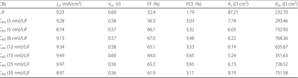
Figure 1 shows the J-V characteristics, recorded under 100 mW/cm2illumination (AM 1.5 G), of the PSCs with and without different thicknesses of C60 sandwiched
between the active layer and 5-nm-thick LiF layer. The device without the C60 layer shows S-shaped curve,
resulting in the low fill factor (FF) and therefore the low PCE, despite the typical short-circuit current density (Jsc) and open-circuit voltage (Voc). The low FF is
ratio-nalized in terms of the insulating property of LiF, which blocks the electron injection/extraction when the LiF layer is too thick and thus leads to the large series resist-ance (Rs) and small shunt resistance (Rsh) of the device
as shown in Table 1 (Rs and Rsh were calculated from
(9.23 mA/cm2) implies that the built-in electric filed in-side the device (from work function difference between anode and cathode) is sufficient to promote the electron transport through LiF (5 nm) CBL by tunneling. After introducing 3-nm-thick C60 layer between P3HT:PCBM
and LiF (5 nm) layers, the S-shape disappears and the FF increases significantly from 32.4 to 56.3%. The increased FF arises from the reduced Rs, which implies that the
C60(3 nm)/LiF (5 nm) bilayer possesses better electrical
conductivity than single LiF (5 nm) layer. With the in-crease of C60thickness, the FF first increases, reaching a
maximum value of 67% at 8 nm and then decreases slightly with further increasing C60thickness. Due to the
recovery of FF, the C60/LiF (5 nm)-based devices show a
maximum PCE of 3.65%, which is two times higher than that (1.79%) of LiF (5 nm)-only device. To demonstrate the reproducibility of the results, the average photovol-taic parameters and standard deviations of the studied devices were calculated from a batch of five devices, as shown in Additional file 1: Table S1. For each device, all the parameters includingJsc,Voc, FF, and PCE are highly
reproducible with little variation, which validates the re-liability of the results presented in Table 1.
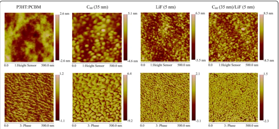
To find out the reasons leading to the high FF for the C60/LiF (5 nm)-based PSCs, AFM measurements
were performed to examine the morphology of the LiF layer on the C60 surface. Figure 2 shows the
height (top) and phase (bottom) images, recorded by tapping mode AFM, of the P3HT:PCBM films without and with the C60 (35 nm), LiF (5 nm), and C60
(35 nm)/LiF (5 nm) layers deposited on top (image size 500 nm × 500 nm). The pristine P3HT:PCBM film exhibits a very smooth surface with a low root-mean-square (rms) roughness of 0.81 nm (height image) and shows fibrillar crystalline domains of P3HT (phase image) [29]. After depositing 35-nm-thick C60 and 5-nm-thick LiF on top, the rms
roughness increases to 1.36 and 1.67 nm, respectively. Although there is no significant difference in rms roughness between the top C60 and LiF layers, the
surface morphologies of these two films are very dif-ferent. The 35-nm-thick C60 shows larger aggregates
(spherical shape) as compared to 5-nm-thick LiF, which can also be observed in their phase images. When depositing the C60 (35 nm)/LiF (5 nm) bilayer
on the P3HT:PCBM film, both the C60 (large size)
and LiF (small size) aggregates are observed, indicat-ing that the underlyindicat-ing C60 layer is not completely
covered by 5-nm-thick LiF. Therefore, some intermix-ing occurs at the C60/LiF interface, which results in
the good electrical conductivity of C60/LiF (5 nm)
bi-layer considering the percolation path formed by C60
molecules.
To further investigate the influence of the C60/LiF
double CBLs on the device performance of PSCs, we fix the C60thickness at the optimum value of 25 nm while
changing the LiF thickness from 0.5 to 8 nm. For com-parison, the devices with LiF single CBL were also fabri-cated. Figure 3 shows the J-V characteristics, recorded under 100 mW/cm2 illumination (AM 1.5 G), of the PSCs using LiF single and C60/LiF double CBLs with
Fig. 1J-Vcharacteristics, recorded under 100 mW/cm2illumination
(AM 1.5 G), of the PSCs with and without different thicknesses of C60
[image:3.595.57.291.87.258.2]inserted between P3HT:PCBM and 5-nm-thick LiF layer
Table 1Photovoltaic parameters for the P3HT:PCBM-based PSCs with and without different thicknesses of C60inserted between the
active layer and 5-nm-thick LiF layer
CBL Jsc(mA/cm2) Voc(V) FF (%) PCE (%) Rs(Ωcm2) Rsh(Ωcm2)
LiF 9.23 0.60 32.4 1.79 87.21 232.70
C60(3 nm)/LiF 9.28 0.58 56.3 3.03 7.74 293.46
C60(5 nm)/LiF 8.74 0.57 66.7 3.32 6.03 732.93
C60(8 nm)/LiF 9.13 0.57 67.0 3.48 6.22 768.36
C60(12 nm)/LiF 9.34 0.58 65.1 3.53 6.14 655.67
C60(15 nm)/LiF 9.49 0.60 64.0 3.65 5.24 351.63
C60(25 nm)/LiF 9.97 0.56 65.3 3.65 6.13 726.52
[image:3.595.58.539.606.732.2]varying thicknesses of LiF. The corresponding photovol-taic parameters of the devices are summarized in Table 2. The devices with LiF single CBL have a maximum PCE of 3.06% at the optimal LiF thickness of 1 nm. Further increasing the thickness leads to a rapid decrease in PCE to 0.79% at 6 nm and 0.06% at 8 nm. In contrast, the devices with C60 (25 nm)/LiF double CBLs exhibit
im-proved performance with a peak efficiency of 3.77% at the LiF thickness of 1 nm. More importantly, as the thickness increases to 6 and 8 nm, PCEs of 2.65 and 1.10% are attained, respectively, which are significantly higher than those of LiF-only devices. It should be men-tioned that the results presented in Table 2 is also highly reproducible, as demonstrated by the very small stand-ard deviations of the device characteristic parameters (Additional file 1: Table S2). For instance, the standard deviation of the device efficiency is less than 0.2% (0.1%
for most devices), indicating high reproducibility. Fur-thermore, the average PCE shows the same trend as ob-served in Table 2, which implies that the comparison of efficiency among different groups is reliable.
As shown in Table 2, the improvement in PCE for the C60 (25 nm)/LiF-based PSCs mainly arises from
the increase in FF and Jsc due to the reduced Rs. To
better understand the Rs reduction, we investigate
the charge transport properties of the LiF single layer and C60/LiF bilayer using the photo-CELIV
technique [30, 31]. Additional file 1: Figure S1 shows the photo-CELIV current transients, recorded at varying voltage rise speeds, for the PSCs with the LiF single and C60/LiF double CBLs. In
photo-CELIV, the time of extraction current maximum (tmax) is used for estimating the charge carrier
mobility according to Eq. 1 [27]. The calculated
Fig. 2Tapping mode AFM height (top) and phase (bottom) images of P3HT:PCBM, P3HT:PCBM/C60(35 nm), P3HT:PCBM/LiF (5 nm), and
P3HT:PCBM/C60(35 nm)/LiF (5 nm) films. The corresponding root-mean-square (rms) roughnesses are 0.81, 1.36, 1.67, and 2.18 nm, respectively
Fig. 3J-Vcharacteristics, recorded under 100 mW/cm2illumination (AM 1.5 G), of the PSCs usingaLiF single andbC
60(25 nm)/LiF double CBLs
[image:4.595.57.540.87.310.2] [image:4.595.57.539.565.703.2]mobilities of the LiF (6 nm)-only device are 3.71, 3.40, and 3.59 × 10⁻⁵ cm2 V−1 s−1 for the voltage slopes of 10, 20, and 30 kV/s, respectively, implying that the mobility is independent on the voltage rise speed. In contrast, the estimated mobilities of the C60 (25 nm)/LiF (6 nm)-based device are 3.81, 3.56,
and 3.09 × 10⁻⁴ cm2 V−1 s−1 for the voltage slopes of 10, 20, and 30 kV/s, respectively, which are one order of magnitude higher than those of the LiF (6 nm)-only device. The increased mobility after introducing a C60 layer can be attributed to the
im-proved electrical conductivity arising from the inter-mixing occurred at the C60/LiF interface. In addition,
it is noted that the photo-CELIV peak for the LiF (6 nm)-only device is broader than that for the C60
(25 nm)/LiF (6 nm)-based device, which indicates a more dispersive charge transport resulting from the larger imbalance between the electron and hole mobilities [32, 33]. This imbalance is attributed to the extremely low electron mobility for the LiF (6 nm)-only device considering that the extraction of electrons is blocked by the thick LiF layer. The accu-mulated electrons at the P3HT:PCBM/LiF interface screen the applied electric field and thereby decrease the rate of charge extraction in the device. In con-trast, the narrow peak for the C60 (25 nm)/LiF
(6 nm)-based device implies the balanced electron and hole mobilities as well as the improved electron extraction owing to the good conductivity of the C60
(25 nm)/LiF (6 nm) bilayer.
Besides the significant improvement in FF, the Jsc is
slightly enhanced after incorporation of C60 (25 nm)
layer. Considering that the spin-coated P3HT:PCBM blend film consists of a P3HT-rich region near the top surface [34, 35], we speculate that the excitons generated in this region can be dissociated at the P3HT/C60
inter-face for C60 (25 nm)/LiF-based devices, which leads to
the increased Jsc compared to the devices without the
C60 interlayer. To verify this speculation, we fabricated
the PSCs with a device structure of ITO/PEDOT:PSS/
P3HT/C60(25 nm)/LiF/Al, where the thickness of P3HT
is varied from 5 to 100 nm. Figure 4 shows the J-V
characteristics of these devices under 100 mW/cm2 illu-mination (AM 1.5 G), and the corresponding photovol-taic parameters are summarized in Additional file 1: Table S3. It is found that theJscof P3HT/C60-based solar
cells increases as the P3HT thickness decreases, which is rationalized in terms of the limited exciton diffusion length in P3HT (~ 10 nm). TheJsc reaches a maximum
value of 1.34 mA/cm2at the P3HT thickness of 10 nm and then drops with further decease of the thickness to 5 nm due to the insufficient absorption. As mentioned above, such P3HT/C60subcell is most likely formed after
depositing 25-nm-thick C60 on top of the P3HT:PCBM
active layer, which results in a 1.34 mA/cm2increase in
Jscunder ideal conditions for C60/LiF-based devices [36].
By comparing the Jsc values of the devices with and
without the C60(25 nm) interlayer, the enhancement in
Jscis around 1 mA/cm2(except for the LiF (8 nm)-based
devices), which is consistent with our speculation. After introducing a C60layer between the P3HT:PCBM
[image:5.595.58.540.110.235.2]and LiF layers, the optical field distribution within the
Table 2Photovoltaic parameters for the P3HT:PCBM-based PSCs using LiF single and C60(25 nm)/LiF double CBLs with different
thicknesses of LiF
CBL Jsc(mA/cm2) Voc(V) FF (%) PCE (%) Rs(Ωcm2) Rsh(Ωcm2)
LiF (0.5 nm) 9.15 0.59 53.8 2.91 5.50 208.94
LiF (1 nm) 9.21 0.58 57.2 3.06 6.14 253.56
LiF (6 nm) 7.20 0.58 18.9 0.79 195.21 62.65
LiF (8 nm) 1.05 0.58 10.2 0.06 4749.92 175.15
C60/LiF (0.5 nm) 10.03 0.59 60.2 3.57 4.95 323.33
C60/LiF (1 nm) 10.10 0.56 66.6 3.77 5.05 626.63
C60/LiF (6 nm) 8.21 0.54 59.8 2.65 8.98 744.54
C60/LiF (8 nm) 6.96 0.54 29.2 1.10 14.08 82.15
Fig. 4J-Vcharacteristics of the PSCs with the device structure of ITO/PEDOT:PSS/P3HT (xnm)/C60(25 nm)/LiF (1 nm)/Al using varying
[image:5.595.306.538.530.693.2]solar cell is most likely altered, which will cause the vari-ation inJsc[26, 37]. To investigate this effect, we first
sim-ulated the electric field intensity inside the P3HT:PCBM active layer for the devices with and without the C60
interlayer. As shown in Additional file 1: Figure S2a, the integrated field intensity for the devices incorporating a C60 layer is weaker in the short-wavelength region and
stronger in the long-wavelength region as compared to the device without C60 interlayer. This trend becomes
more remarkable, and simultaneously, a red shift is ob-served with increasing the C60thickness. Additional file 1:
Figure S2b shows the absorption spectra of the pristine C60film, and the P3HT:PCBM films with and without
dif-ferent CBLs deposited on top. Comparing the absorption spectra of P3HT:PCBM/C60 (25 nm) films with and
without 8-nm-thick LiF, the two curves overlap almost completely, indicating that LiF does not absorb visible light. On the other hand, the P3HT:PCBM/C60films have
higher absorption in the wavelength ranges of 400~510 nm and 580~680 nm when compared to the pristine P3HT:PCBM film. This absorption enhancement becomes more pronounced with increasing C60thickness. Intuitively,
the absorption enhancement in the 400~510 nm wave-length range arises from the C60absorption (400~550 nm).
Additional file 1: Figure S2c shows the incident photon-to-current conversion efficiency (IPCE) spectra of the PSCs with LiF (5 nm) single and C60(25 nm)/LiF (5 nm) double
CBLs. Compared to the LiF-only device, the device with C60/LiF double CBLs has a lower IPCE at the short
wave-lengths due to the parasitic absorption in the C60film, and
shows a higher IPCE at long wavelengths, owing to the op-tical spacer effect as well as the contribution of P3HT/C60
subcell.
From Table 2, it is noticed that the C60 (25 nm)/
LiF (8 nm)-based device exhibits a low PCE of 1.10% although this efficiency is still much higher than that (0.06%) of the LiF (8 nm)-only device. The low PCE is the result of the small Jsc and FF, which is caused
by the large Rs. As discussed above, the C60 (35 nm)/
LiF (5 nm) film has good electrical conductivity due to the formation of the mixed morphology between C60 and LiF layers (see Fig. 2). To find the reason for
the high resistance of the C60 (25 nm)/LiF (8 nm)
film, AFM measurements were performed on P3HT:PCBM films without and with the C60 (25 nm),
LiF (8 nm), and C60 (25 nm)/LiF (8 nm) layers
depos-ited on top. As shown in Additional file 1: Figure S3, large spherical aggregates are formed in the C60
(25 nm) film while relatively small aggregates are formed in the LiF (8 nm) film, which is similar to the observation in Fig. 2. When depositing 8-nm-thick LiF on top of the C60 (25 nm) layer, the morphology
(small aggregates) is very similar to that of the pris-tine LiF film, indicating that the underlying C60
aggregates are completely covered by 8-nm-thick LiF. Therefore, we speculate that a thick LiF accumulates at the top of the C60 (25 nm)/LiF (8 nm) bilayer film,
which hinders the electron extraction and therefore leads to the high Rs of the device.
Conclusions
In summary, we have demonstrated that a thick LiF can be used as CBL in P3HT:PCBM-based PSCs by simply introducing a C60 layer between the active
layer and the LiF layer. The devices with the C60/LiF
(5 nm) double CBLs exhibit a peak efficiency of 3.65%, while the LiF (5 nm)-only device shows a two times lower PCE of 1.79%. The improved device performance mainly results from the high FF due to the good electrical conductivity of the C60/LiF bilayer.
In addition, the Jsc is also improved after introducing
a C60 interlayer, which can be attributed to the
con-tribution of P3HT/C60 subcell as well as the optical
spacer effect of C60. Further increasing the LiF
thick-ness to 8 nm leads to the rapid decrease of PCE to 1.10 and 0.06% for the C60/based device and
LiF-only device, respectively. The decline in PCE of the device with C60/LiF (8 nm) double CBLs is caused by
the impeded electron transport, owing to the accumu-lated LiF at the top of the C60 (25 nm)/LiF (8 nm)
bi-layer. All in all, these results indicate that the C60/LiF
bilayer is a more promising CBL as compared to LiF single layer for fabricating highly efficient and large-scale PSCs.
Additional file
Additional file 1:Supporting information.Table S1.Average photovoltaic performance parameters for the P3HT:PCBM-based PSCs with and without different thicknesses of C60inserted between the active layer and 5-nm-thick
LiF layer.Table S2.Average photovoltaic performance parameters for the P3HT:PCBM-based PSCs using LiF single and C60(25 nm)/LiF double CBLs with
different thicknesses of LiF.Figure S1.Photo-CELIV curves for the devices with (a) the LiF (6 nm) single and (b) C60(25 nm)/LiF (6 nm) double CBLs. Table S3.Photovoltaic parameters of the P3HT/C60(25 nm)-based PSCs with
the P3HT thickness varied from 5 to 100 nm.Figure S2.(a) Simulated electric field intensity within the active layer versus the thickness of C60interlayer for
the PSCs having the following structure: ITO (150 nm)/PEDOT:PSS (45 nm)/ P3HT:PCBM (180 nm)/C60(xnm)/Al (120 nm). (b) Absorption spectra of the
pristine C60film and the P3HT:PCBM blend films with and without different CBLs
deposited on top. (c) Incident photon-to-current conversion efficiency (IPCE) spectra for the devices with and without the C60interlayer.Figure S3.AFM
height (top) and phase (bottom) images of C60(25 nm), LiF (8 nm), and C60
(25 nm)/LiF (8 nm) layers deposited on P3HT:PCBM blend films. (DOC 1663 kb)
Acknowledgements
This work was supported by the National Natural Science Foundation of China (61604101) and the Scientific Research Foundation of UESTC for Young Teacher (ZYGX2016KYQD134).
Authors’Contributions
Competing Interests
The authors declare that they have no competing interests.
Publisher’s Note
Springer Nature remains neutral with regard to jurisdictional claims in published maps and institutional affiliations.
Author details
1School of Optoelectronic Information, University of Electronic Science and Technology of China (UESTC), Chengdu 610054, People’s Republic of China. 2Center for Applied Chemistry, University of Electronic Science and Technology of China (UESTC), Chengdu 610054, People’s Republic of China. 3Department of Electrical Engineering and Computer Science, The University of Michigan, 1301 Beal Ave., Ann Arbor, MI 48109, USA.
Received: 4 July 2017 Accepted: 30 August 2017
References
1. Yu G, Gao J, Hummelen JC, Wudl F, Heeger AJ (1995) Polymer photovoltaic cells: enhanced efficiencies via a network of internal donor-acceptor heterojunctions. Science 270:1789–1791
2. Li G, Zhu R, Yang Y (2012) Polymer solar cells. Nat Photonics 6:153–161 3. Li YF (2012) Molecular design of photovoltaic materials for polymer solar
cells: toward suitable electronic energy levels and broad absorption. Acc Chem Res 45:723–733
4. Park HJ, Kang MG, Ahn SH, Guo LJ (2010) A facile route to polymer solar cells with optimum morphology readily applicable to a roll-to-roll process without sacrificing high device performances. Adv Mater 22:E247–E253 5. Xu G, Shen L, Cui C, Wen S, Xue R, Chen W, Chen H, Zhang J, Li H, Li Y, Li YF
(2017) High-performance colorful semitransparent polymer solar cells with ultrathin hybrid-metal electrodes and fine-tuned dielectric mirrors. Adv Funct Mater 27:1605908
6. Zhao J, Li Y, Yang G, Jiang K, Lin H, Ade H, Ma W, Yan H (2016) Efficient organic solar cells processed from hydrocarbon solvents. Nat Energy 1:15027 7. Yang L, Zhang S, He C, Zhang J, Yao H, Yang Y, Zhang Y, Zhao W, Hou J
(2017) New wide band gap donor for efficient fullerene-free all-small-molecule organic solar cells. J Am Chem Soc 139:1958–1966
8. Bin H, Gao L, Zhang ZG, Yang Y, Zhang Y, Zhang C, Chen S, Xue L, Yang C, Xiao M, Li YF (2016) 11.4% Efficiency non-fullerene polymer solar cells with trialkylsilyl substituted 2D-conjugated polymer as donor. Nat Commun 7:13651 9. Yang Y, Zhang ZG, Bin H, Chen S, Gao L, Xue L, Yang C, Li YF (2016)
Side-chain isomerization on an n-type organic semiconductor ITIC acceptor makes 11.77% high efficiency polymer solar cells. J Am Chem Soc 138:15011–15018
10. Kuzmich A, Padula D, Ma H, Troisi A (2017) Trends in the electronic and geometric structure of non-fullerene based acceptors for organic solar cells. Energy Environ Sci 10:395–401
11. Fan Q, Su W, Meng X, Guo X, Li G, Ma W, Zhang M, Li YF (2017) High-performance non-fullerene polymer solar cells based on fluorine substituted wide bandgap copolymers without extra treatments. Sol RRL 1:1700020 12. Gasparini N, Lucera L, Salvador M, Prosa M, Spyropoulos GD, Kubis P,
Egelhaaf H-J, Brabec CJ, Ameri T (2017) High-performance ternary organic solar cells with thick active layer exceeding 11% efficiency. Energy Environ Sci 10:885–892
13. He Z, Zhong C, Su S, Xu M, Wu H, Cao Y (2012) Enhanced power-conversion efficiency in polymer solar cells using an inverted device structure. Nat Photonics 6:593–597
14. Yip H-L, Jen AKY (2012) Recent advances in solution-processed interfacial materials for efficient and stable polymer solar cells. Energy Environ Sci 5:5994–6011
15. Li W, Yan D, Liu W, Chen J, Xu W, Zhan C, Yao J (2017) A new function of N719: N719 based solution-processible binary cathode buffer layer enables high-efficiency single-junction polymer solar cells. Sol RRL 1:1700014 16. Zhao F, Wang Z, Zhang J, Zhu X, Zhang Y, Fang J, Deng D, Wei Z, Li YF,
Jiang L, Wang C (2016) Self-doped and crown-ether functionalized fullerene as cathode buffer layer for highly-efficient inverted polymer solar cells. Adv Energy Mater 6:1502120
17. Liu X, Jiao W, Lei M, Zhou Y, Song B, Li YF (2015) Crown-ether functionalized fullerene as a solution-processable cathode buffer layer for high performance perovskite and polymer solar cells. J Mater Chem A 3:9278–9284
18. Lee JY, Lee T, Park HJ, Guo LJ (2014) Improved solar cell performance by adding ultra-thin Alq3at the cathode interface. Org Electron 15:2710–2714
19. Liu D, Li S, Zhang P, Wang Y, Zhang R, Sarvari H, Wang F, Wu J, Wang Z, Chen ZD (2017) Efficient planar heterojunction perovskite solar cells with Li-doped compact TiO2layer. Nano Energy 31:462–468
20. Li S, Zhang P, Chen H, Wang Y, Liu D, Wu J, Sarvari H, Chen ZD (2017) Mesoporous PbI2assisted growth of large perovskite grains for efficient
perovskite solar cells based on ZnO nanorods. J Power Sources 342:990–997 21. Chen H, Liu D, Wang Y, Wang C, Zhang T, Zhang P, Sarvari H, Chen Z, Li S
(2017) Enhanced performance of planar perovskite solar cells using low-temperature solution-processed Al-doped SnO2as electron transport layers.
Nanoscale Res Lett 12:238
22. Brabec CJ, Shaheen SE, Winder C, Sariciftci NS, Denk P (2002) Effect of LiF/metal electrodes on the performance of plastic solar cells. Appl Phys Lett 80:1288–1290 23. Li G, Chu CW, Shrotriya V, Huang J, Yang Y (2006) Efficient inverted polymer
solar cells. Appl Phys Lett 88:253503
24. Apilo P, Hiltunen J, Välimäki M, Heinilehto S, Sliz R, Hast J (2015) Roll-to-roll gravure printing of organic photovoltaic modules-insulation of processing defects by an interfacial layer. Prog Photovolt Res Appl 23:918–928 25. Liu X, Yu H, Yan L, Dong Q, Wan Q, Zhou Y, Song B, Li YF (2015) Triple cathode
buffer layers composed of PCBM, C60, and LiF for high-performance planar
perovskite solar cells. ACS Appl Mater Interfaces 7:6230–6237
26. Liu X, Lee JY, Guo LJ (2013) Efficiency and stability enhancement of polymer solar cells using multi-stacks of C60/LiF as cathode buffer layer.
Org Electron 14:469–474
27. Juška G, Arlauskas K, Viliūnas M, Kočka J (2000) Extraction current transients: new method of study of charge transport in microcrystalline silicon. Phys Rev Lett 84:4946–4949
28. Dennler G, Mozer AJ, Juška G, Pivrikas A, Österbacka R, Fuchsbauer A, Sariciftci NS (2006) Charge carrier mobility and lifetime versus composition of conjugated polymer/fullerene bulk-heterojunction solar cells. Org Electron 7:229–234
29. Shrotriya V, Yao Y, Li G, Yang Y (2006) Effect of self-organization in polymer/fullerene bulk heterojunctions on solar cell performance. Appl Phys Lett 89:063505
30. Park M-H, Li J-H, Kumar A, Li G, Yang Y (2009) Doping of the metal oxide nanostructure and its influence in organic electronics. Adv Funct Mater 19:1241–1246
31. Tremolet de Villers B, Tassone C, Tolbert JSH, Schwartz BJ (2009) Improving the reproducibility of P3HT:PCBM solar cells by controlling the PCBM/ cathode interface. J Phys Chem C 113:18978–18982
32. Chellappan V, Ng GM, Tan MJ, Goh W-P, Zhu F (2009) Imbalanced charge mobility in oxygen treated polythiophene/fullerene based bulk heterojunction solar cells. Appl Phys Lett 95:263305
33. Kumar A, Liao H-H, Yang Y (2009) Hole mobility in optimized organic photovoltaic blend films obtained using extraction current transients. Org Electron 10:1615–1620
34. Kumar A, Li G, Hong Z, Yang Y (2009) High efficiency polymer solar cells with vertically modulated nanoscale morphology. Nanotechnology 20:165202 35. Sun XW, Zhao DW, Ke L, Kyaw AKK, Lo GQ, Kwong DL (2010) Inverted
tandem organic solar cells with a MoO3/Ag/Al/Ca intermediate layer. Appl
Phys Lett 97:053303
36. Zhang C, Tong SW, Jiang C, Kang ET, Chan DSH, Zhu C (2008) Simple tandem organic photovoltaic cells for improved energy conversion efficiency. Appl Phys Lett 92:083310
37. Hadipour A, Cheyns D, Heremans P, Rand BP (2011) Electrode