N A N O E X P R E S S
Open Access
Resistive and New Optical Switching Memory
Characteristics Using Thermally Grown Ge
0.2
Se
0.8
Film in Cu/GeSe
x
/W Structure
Debanjan Jana, Somsubhra Chakrabarti, Sheikh Ziaur Rahaman and Siddheswar Maikap
*Abstract
It is known that conductive-bridge resistive-random-access-memory (CBRAM) device is very important for future high-density nonvolatile memory as well as logic application. Even though the CBRAM devices using different materials, structures, and switching performance have been reported in Nanoscale Res. Lett., 2015, however, optical switching characteristics by using thermally grown Ge0.2Se0.8film in Cu/GeSex/W structure are reported for the first time in this study. The Cu/GeSex/W memory devices have low current compliances (CCs) ranging from 1 nA to 500μA with low voltage of ±1.2 V, high resistance ratio of approximately 103, stable endurance of >200 cycles, and good data retention of >7 × 10³s at 85 °C. Multi-steps of RESET phenomena and evolution of Cu filaments’shape under CCs ranging from 1 nA to 500μA have been discussed. Under external white-light illumination with an intensity of 2.68 mW/cm2(wavelength ranges from 390 to 700 nm), memory device shows optical switching with long read pulse endurance of >105cycles. This CBRAM device has optically programmed and electrically erased, which can open up a new area of research field for future application.
Keywords:Optical switching; Resistive switching; Light illumination; CBRAM; GeSex
Background
Recently, the conductive-bridge resistive-random-access-memory (CBRAM) device is considered among the most promising solutions for future low-cost embedded non-volatile memories [1–5]. Although several solid-electrolyte materials such as GeS2 [6], GeTe [7], Ag2S
[8, 9], and GeSe [10–13] have been reported to explore CBRAM performances and switching mechanism, how-ever, light-induced resistive switching phenomena of different materials have been reported few. Sun et al. [14] have reported white-light illuminated resistive switch-ing behavior usswitch-ing Ag/NiWO4/Ti structure. The device is
operated under a current of 50 μA. Mou et al. [15] have investigated light illumination effect on Ag/Ag2S/Au
CBRAM device. It has been reported that turn-off volt-age decreases from −0.8 to −0.25 V which might be ef-fect of change of reduction potential of Ag ion under external light. In addition, Retamal et al. [16] have
reported the unipolar resistive switching characteristics and variation reduced of resistance states of Pt/ZnO/Pt structure under ultraviolet light illumination with a high RESET current of 5 mA. Liu et al. [17] have re-ported unipolar resistive switching characteristics using ITO/HfOx/TiN structure under ultraviolet light
expos-ure with a high RESET current of >5 mA. The resistive switching phenomena occur owing to oxygen vacancy generation during light illumination. It is realized that a study on resistive switching phenomena of solid-electrolyte material under external light is very import-ant to design high-density memory in future. According to this, we have also reported impact of white-light illu-mination on GeSex-based CBRAM devices previously
[18]. However, resistive switching phenomena and new optical switching by using thermally grown Ge0.2Se0.8
material in Cu/GeSex/W structure have been reported
here. The memory device shows bipolar resistive switch-ing phenomena with CCs rangswitch-ing from 1 nA to 500 μA under small operation voltage of ±1.2 V, high resistance ratio of approximately 103, good endurance of >200 cy-cles, and good data retention of >7 × 10³ s at 85 °C. * Correspondence:[email protected]
Thin Film Nano Technology Laboratory, Department of Electronic Engineering, Chang Gung University, 259 Wen-Hwa 1st Rd., Kwei-Shan, Tao-Yuan 333, Taiwan
Multi-step RESET characteristics and filaments’ shape with CCs ranging from 1 nA to 500 μA have been ex-plained. The device structure and GeSex film are
con-firmed by transmission electron microscope (TEM) and energy-dispersive X-ray spectroscopy (EDX) analysis. After white-light illumination with an intensity of 2.68 mW/cm2 on the Cu electrode of the via-hole re-gion, optical switching is observed owing to Cu ion mi-gration through GeSex solid electrolyte as well as
stronger Cu filament being formed. Memory device performs good data retention and long read pulse en-durance of >105cycles after white-light illumination.
Methods
Tungsten (W) with a thickness of 100 nm was deposited on a SiO2/Si wafer. To form via-hole devices, a SiO2
layer with a thickness of 150 nm was deposited on W bottom electrode (BE). The via-holes were fabricated by using standard lithography and etching processes. To follow the lift-off process, the photoresist was coated after formation of the via-holes. Then, the Ge0.4Se0.6
solid-electrolyte material with a thickness of approxi-mately 40 nm was deposited by thermal evaporator. Prior to deposition of GeSex film, the chamber pressure
was 5 × 10⁻⁶ Torr. The small pieces of Ge0.4Se0.6 were
used for evaporation. It is realized that the percentage of selenium was greater than 60 % in the GeSex solid
elec-trolyte (or Se-rich GeSe film) because melting point of Se is much lower than the Ge (221 °C vs. 938.2 °C). A copper (Cu) film with a thickness of approximately 150 nm was deposited in situ by the same thermal evap-orator. Finally, lift-off process was performed to fabricate the Cu/GeSex/W device. Figure 1a shows a TEM image
of Cu/GeSex/W CBRAM device. To confirm the
deposition of GeSex film, a typical size of 0.2 × 0.2 μm2
is shown. The layer-by-layer structure is observed clearly. The thicknesses of GeSex and Cu layers are
found to be approximately 39 and 150 nm, respectively. The thickness of W electrode is approximately 90 nm. Figure 1b shows EDX spectrum of GeSex layer which
confirms the Ge and Se contents. Memory characteris-tics were measured by using Agilent 4156C semicon-ductor parameter analyzer. White light through optical microscope was applied vertically on Cu TE of the via-hole region. The light intensity was 2.68mW/cm2 and visible wavelengths were390–700 nm. When the device is under illumination, the main portion of GeSex film
which was covered by Cu is under darkness because the light was illuminated on Cu TE. However, the light could be transmitted through thinner sidewall of via-hole to the GeSex film. After applying light on HRS of the
CBRAM devices, the RESET current was measured by applying negative sweeping bias on the Cu TE. The bias was applied on the Cu TE, and W BE was grounded dur-ing measurement.
[image:2.595.60.539.515.704.2]Results and Discussion
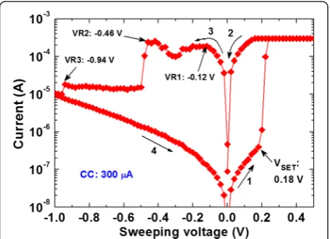
Figure 2 shows typical current–voltage (I-V) characteris-tic of the Cu/GeSex/W memory device with a device size
of 2 × 2 μm2. The sweeping voltage is 0 V→+1 V→ 0 V→−1 V→0 V, which is shown by arrows 1→4. This device is operated with a small voltage of ±1.2 V and the current compliance (CC) is 300μA. For this de-vice, forming process is not needed because GeSex is
solid electrolyte and the film contains a porous material. Therefore, Cu ions can be migrated easily under external low bias as well as formation process can be exempted. A low RESET current (IRESET) of approximately 190μA
Fig. 1TEM and EDX analysis.aTEM image of Cu/GeSex/W CBRAM device.bEnergy-dispersive X-ray spectrum shows presence of Ge and Se elements
is observed. Both the hold and delay times were 100μs. The SET voltage (VSET) is 0.18 V, which is almost the
same value for a Cu/Ge0.2Se0.8/W structure [19]. The
values of HRS and LRS are found to be 7.2 MΩ and 0.51 kΩat a read voltage of 50 mV, respectively. A high resistance ratio (HRS/LRS) of >103is obtained, which is very useful for high-density memory application. By ap-plying a smallVSET of >0.18 V on the Cu electrode, the
Cu ions are generated at the GeSex/Cu interface and
mi-grated towards the W BE under electric field. The Cu metal starts to grow from the W BE to form conical-shaped metallic Cu filament in the GeSexsolid electrolyte.
As a CC of 300 μA, the conducting filament has a shape of conical or pyramid type. The base of filament is on the inert electrode surface and the neck is at the GeSex/Cu
interface. By applying negative bias on Cu electrode, this device shows multiple RESETs at VR1 =−0.12 V, VR2 =−0.46 V, and VR3 =−0.94 V. At−0.12 V, an elec-trochemical oxidation (Cu→Cuz++ ze−, wherez= 1 or 2) process has been started at the GeSex/Cu interface
through joule heating, which results in Cu filament starting to dissolve. The current is also decreasing up to −0.3 V because Cu ions are migrated towards Cu electrode as well as the dissolution length of filament is increased. As long as there is sufficient gap in between Cu and filament at a voltage of −0.3 V, more Cu ions will be also generated from the GeSex/filament interface
because the diameter is increased towards the W electrode by applying higher negative bias of <0.3 V. In this case, huge Cu ions can be gathered at the Cu/GeSex interface,
which results in a re-growth of filament as well as current increasing up to VR2 of−0.46 V. The re-growth phenom-ena of a metallic filament are also reported in our previous study by using GeOxor Ta2O5material [20]. By applying
higher negative voltage of <−0.46 V, a strong electro-chemical oxidation with joule heating happened and LRS changes to HRS. The dissolved length of conduct-ing filament is gradually increased up to VR3 of−1 V. Still, the filament remains because of the conical shape.
[image:3.595.57.292.89.259.2]I-V curve shows that LRS is ohmic behavior (IαV) whereas HRS follows trap-assisted space charge-limited current conduction behavior (IαV and IαV2). It is real-ized that the shape of Cu filament changes with differ-ent CCs, which is also important to understand and this has been explained below.
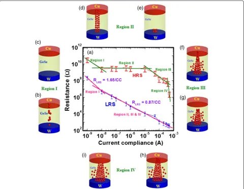
Figure 3 represents the CC dependence HRS and LRS distribution. The current is varied from 1 nA to 500μA. Schematic views of different-shaped filaments are also shown. Both values of LRS and HRS are decreased with increasing CC owing to stronger and different-shaped metallic filaments (Fig. 3a). Two distinct regions of LRS are observed. Region I is defined with CCs from 1 to 10 nA (RLRS= 1.65/CC). In region II, the current is
var-ied from 10 nA to 500 μA (RLRS= 0.87/CC). In the case
of HRS, current compliance depends on four regions where“region I” is defined from 1 to 10 nA,“region II” from 50 nA to 10 μA, “region III” from 50 to 300 μA, and “region IV”from 400 to 500μA. It is assumed that different shapes of filament are formed after SET, which will create asymmetric HRS distribution after RESET op-eration. Therefore, the filament shapes are created artis-tically by relative observation of HRS values. In region I, the values of both HRS and LRS are quite high which may cause that continuous Cu metallic filament will not be formed at a low current of <10 nA. A chain-type fila-ment is possible to form or Cu nanocrystals can be formed in the GeSexsolid electrolyte under SET (Fig. 3b).
A silver (Ag) nanocrystal filament in SiOx or AlOx film
was also reported by Yang et al. [21]. The value of LRS is higher owing to filament resistance added with bulk resistance of GeSex solid electrolyte. At CC of 1 nA,
total filament is dissolved after RESET because the value of HRS is almost the same with pristine one (Fig. 3c). However, the values of both HRS and LRS decrease up to CC of 10 nA and a small filament length remains after RESET. In region II, the value of LRS decreases whereas HRS is independent of CCs. This implies that a cylindrical filament is formed up to CC of 10 μA, as shown in Fig. 3d. Only a small length of filament re-mains after RESET, as shown in Fig. 3e. In region III, the value of HRS decreases again up to CC of 300μA owing to conical-shaped filament (Fig. 3f ), as mentioned in I-V characteristics above. After RESET, the neck side of this conical-shaped filament is dissolved, i.e., a longer length of filament remains on the W BE (Fig. 3g). That is why the value of HRS is decreased. This conical-shaped Cu filament is observed in AlOx-based material by Celano
et al. [22]. This is like an interface-type switching Fig. 2Current–voltage characteristics. Current–voltage hysteresis
phenomena of thermally deposited GeSexfilm in Cu/GeSex/W
because the filament is formed/dissolved at the GeSex/
Cu interface. In region IV, the value of LRS is decreased by increasing CC up to 500 μA because the conical-shaped diameter is increased further (Fig. 3h). However, the HRS is decreased too after RESET (Fig. 3i). This sug-gests that the leakage current through the dissolved re-gion is increased because of larger diameter of the remaining filament. In this case, resistive ratio will be controlled by forming/dissolving the metallic filament at the GeSex/Cu interface. A higher resistance ratio of
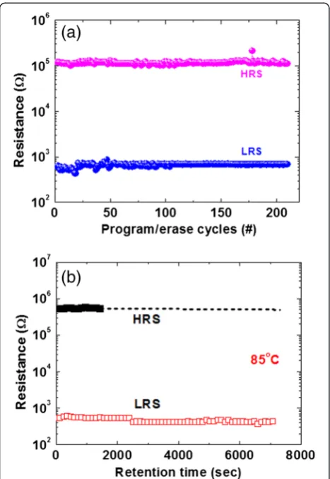
ap-proximately 103 can be observed from CC of 10– 300 μA. This CBRAM device has stable program/erase (P/E) endurance of >200 cycles and good data retention of >7000 s at 85 °C, as shown in Fig. 4. Low P/E voltages and currents were +1/−1.2 V and 500 μA/1 mA,
respectively (Fig. 4a). A read voltage is 50 mV. The P/E pulse width is 500 μs. Stable resistance ratio of >200 is obtained, which is lower than the mentioned as in I-V characteristics. Generally, the value of HRS is decreased after few cycles, as reported previously [12], however this thermally grown GeSex film has benefit to have
un-changed HRS even after 200 cycles. To obtain stable program/erase (P/E) cycles, good structure with a switching material is necessary to design, which is ob-served here. By adjusting the P/E operation conditions, the filament length or maintaining dissolution gap is also important where the resistance ratio could be decreased because HRS value will be lower. Stable P/E cycles are obtained because major contribution is switching mater-ial in a designed structure. Therefore, the stable HRS Fig. 3HRS/LRS vs. current compliance.aDistribution of HRS and LRS with different current compliances ranging from 1 nA to 500μA is shown. Different shapes of the Cu filaments are identified by observing the current compliance dependent of both LRS and HRS. Evolution of Cu filament formation and dissolution with different CCs is shown schematically in (b–i). At region I, a Cu nano-chain is formed underbSET andcdissolution under RESET. At region II, a cylindrical filament could bedformed andeunder SET and RESET, respectively. At region III, a conical filament could be formed in the GeSexfilm and dissolved at the Cu/GeSexinterface underfSET andgRESET conditions.hA stronger conical-shaped filament could be
[image:4.595.58.539.89.461.2]characteristic is observed because of this thermally grown GeSex film in the Cu/GeSex/W structure. It is
also possible to have different stoichiometry GeSex film
deposited by thermal evaporation which has also key role to have stable HRS. The retention characteristics of our resistive switching memory device are shown in Fig. 4b. An unchanged resistance ratio of approximately 103at 85 °C has been observed after 7000 s owing to the strong Cu metallic filament formation into the GeSex
solid electrolyte. It is true that HRS value is stable after 1500 s. Due to time limitation of the HP 4156C system, longer time is not dedicated for evaluation. It is interest-ing to note that this CBRAM device can be programmed by using external white light and erased by using nega-tive bias on the Cu electrode, which have been discussed for the first time below.
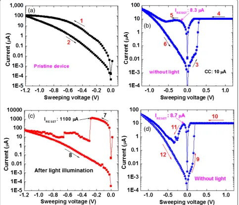
Figure 5 shows I-V characteristics with and without external white light on Cu/GeSex/W CBRAM device.
Evolution ofI-Vhysteresis measurement is shown by ar-rows from 1→12. Figure 5a shows the initial I-V
characteristics at negative region without light or pris-tine state. Even though there is no prominent RESET current, however, leakage current is decreased after applying negative bias of −1.2 V (i.e., arrows 1→2). This suggests that there is some diffusion of Cu with-out bias of >VSETor external light. It indicates that the
device is keeping in environment some days and Cu diffusion may be possible. Figure 5b showsI-V charac-teristics with a low CC of 10 μA and low operation voltage of ±1.2 V is applied with sweeping direction 3→6 (i.e., 0 V→+1.2 V→0 V→−1.2 V→0 V). A low RESET voltage of−0.18 V andIRESETof 8.3μA are
observed. Now, this device is at HRS and white light is turned on for approximately 10 s. Then, it is turned off. All measurements were performed at room temperature (25 °C).I-Vhysteresis characteristics are shown by arrows 7→8 (i.e., 0 V→−1.2 V→0 V), as shown in Fig. 5c. The RESET voltage (VR1) and IRESETare found to be −0.3 V
and 1100 μA, respectively. It implies that external light can influence the Cu diffusion into GeSexsolid electrolyte
and makes stronger Cu metallic filament from BE to TE resulting to memory device switches from HRS to LRS. Light stimulates the Cu/GeSex interface and Cu ions are
created. The Cu ions have been diffused by this stimulated light energy. Therefore, this needs longer time of >5 s from higher resistance value to lower resistance value. Due to our limitation of lab facility, one light source with a high intensity of 2.68 mW/cm2 was used. Therefore, more Cu diffusion into the GeSexfilm as well as stronger
filament is formed. Further study is needed to control Cu diffusion as well as filament diameter or RESET current could be controlled. Obviously, if the LRS value is low, then the RESET voltage will be also small; especially RESET voltage for the CBRAM devices is small [1]. A large resistance ratio of >105 is observed because of higher RESET current. Due to this high resistance ratio, multi-level cell operation can be obtained by control-ling external light. Again, the device shows also normal bipolar resistive switching characteristics without light, as shown in Fig. 5d. This indicates that this device can be programmed by external white light and erased by external negative bias on the Cu TE. Therefore, optical switching is observed and it may open up new research field for external light effect on the CBRAM devices. This optical switching is nonvolatile. The retention characteristics of the Cu/GeSex/W CBRAM devices are
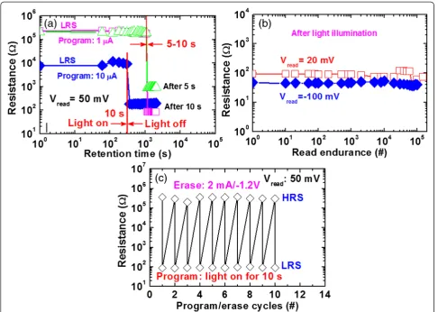
shown in Fig. 6a. Stable retention characteristics are observed after CCs of 1 and 10μA and also after light illumination. Both values of LRS are suddenly de-creased after light turning on time of 5–10 s. The de-vice is programmed first at 1μA. The data retention is measured up to 1080 s. Then, light is illuminated on via-hole region for a duration of 5 or 10 s. The resis-tances after illumination of 5 and 10 s are approximately Fig. 4Endurance and data retention characteristics. aStable P/E
endurance of >200 cycles of the Cu/GeSex/W structure is obtained.
[image:5.595.57.291.88.427.2]1 kΩ and 100 Ω, respectively. Due to this LRS value changes with different light durations, light turned on time will control also multi-level cell operation. Unfortu-nately, the illumination time could not be observed dir-ectly from this data retention measurement because read out was every 60 s. However, the light turned ontimeis shown in Fig. 6a. After RESET the device by applying negative bias, the device is programmed at 10μA. It is noticed that the LRS values are approximately 10 and 300 kΩfor the CCs of 1 and 10 μA, respectively. This is due to the smaller filament diameter at CC of 1μA than the filament diameter at a CC of 10μA. The data reten-tion is measured up to 300 s. Then, suddenly, the light is turned on manually for a duration of 10 s. The LRS value changes to approximately 187Ω. The LRS value is
shown stable after light turned off up to 2000 s. After light illumination, the data retention is also continued to measure up to 2000 s. After light illumination, the LRS value does not change with time. So, the data retention is good because stronger Cu filament is formed. It shows that the LRS value changes to lower value depending on light illumination time because stronger Cu filament is formed after time being light energy stimulates Cu ion to migrate through GeSex layer. Good pulse endurance
[image:6.595.57.541.91.505.2]on Ag/Ag2S/Au structure [15]. Figure 6c shows program/
erase endurance under programming by light illumin-ation of 10 s and erasing by RESET voltage. This P/E endurance is performed manually because of no auto-system in our lab. It is expected that longer P/E cycles can be obtained in the future. Therefore, the Cu/GeSex/
W CBRAM devices could be programmed by external light and erased by electrical bias on the Cu TE. Basic-ally, the erase operation can be controlled by external current (>IRESET) and voltage (<VRESET). However, the
RESET operation will have also high-speed operation of few nanoseconds [1]. So, external light impacts the de-vice switching, which is also very useful for a new area of research.
Conclusions
Resistive and new optical switching characteristics using thermally grown GeSex solid electrolyte in Cu/GeSex/W
structure have been investigated. The CBRAM device shows multi-step RESET phenomena at a CC of 300μA
with a low operation voltage of ±1.2 V, high resistance ratio of >104, stable endurance of >200 cycles, and good data retention of >7 × 10³s at 85 °C. Evolution of Cu fil-aments’shape under CCs ranging from 1 nA to 500μA has been understood by observing both of HRS and LRS. The device changes the HRS to LRS under white-light illumination on it, which attributes to the Cu ion migration through the GeSex solid electrolyte and form
Cu metallic path. After light illumination, memory de-vice shows good data retention of >103 s and long read pulse endurance of >105 cycles. This suggests that this GeSex-based CBRAM device has great potential for
fu-ture light-controlled optical switching and may open up a new area of research.
Competing Interests
The authors declare that they have no competing interests.
Authors’Contributions
DJ wrote the first draft. SC helped to modify the manuscript. SZR fabricated and measured the memory devices without light. Both DJ and SC helped also to measure the devices. SM measured the memory devices with white
Fig. 6Data retention and read endurance after light illumination.aBoth values of LRS after programming at CC of 1 and 10μA are decreased when external white light is turned on with time duration of 5–10 s, which is owing to stronger Cu filament being formed.bRead pulse endurance of >105cycles is observed after light illumination.cThe device shows program/erase endurance by external light illumination of 10 s
[image:7.595.56.543.88.434.2]light. This research work was carried out under the instruction of SM. The paper has been thoroughly written and modified by SM. All the authors contributed to the revision of the manuscript. All authors read and approved the final manuscript.
Acknowledgements
This work was supported by the National Science Council (NSC) Taiwan, under contract nos. NSC-102-2221-E-182-057-MY2, 97-2221-E-182-051-MY3, andMOST-104-2221-E-182-075. The name of NSC has been changed to Ministry of Science and Technology (MOST), Taiwan. The authors are grateful to EOL/ITRI, Hsinchu, Taiwan for their experimental support.
Received: 13 April 2015 Accepted: 25 September 2015
References
1. Jana D, Roy S, Panja R, Dutta M, Rahaman SZ, Mahapatra R, et al. Conductive-bridging random-access-memory: challenges and opportunity for 3D architecture. Nanoscale Res Lett. 2015;10:188.
2. Waser R, Aono M. Nanoionics-based resistive switching memories. Nat Mater. 2007;6:833.
3. Chen A. Ionic memory technology, Solid State Electrochemistry II. 2011. p. 1–30.
4. Kim KH, Gaba S, Wheeler D, Cruz-Albrecht JM, Hussain T, Srinivasa N, et al. A functional hybrid memristor crossbar-array/CMOS system for data storage and neuromorphic applications. Nano Lett. 2012;12:389.
5. Valov I, Waser R, Jameson JR, Kozicki MN. Electrochemical metallization memories—fundamentals, applications, prospects. Nanotechnology. 2011;22:254003.
6. Vianello E, Molas G, Longnos F, Blaise P, Souchier E, Cagil C, et al. Sb-doped GeS2as performance and reliability booster in conductive bridge RAM. Tech
Dig- Electron Device Meeting. 2012;31:5–1.
7. Banno N, Sakamoto T, Iguchi N, Sunamura H, Terabe K, Hasegawa T, et al. Diffusivity of Cu ions in solid electrolyte and its effect on the performance of nanometer-scale switch. IEEE Trans Electron Devices. 2008;55:3283. 8. Xu Z, Bando Y, Wang W, Bai X, Golberg D. Real-time in situ HRTEM-resolved
resistance switching of Ag2S nanoscale ionic conductor. ACS Nano.
2010;4:2515.
9. Terabe K, Hasegawa T, Nakayama T, Aono M. Quantized conductance atomic switch. Nature. 2005;433:47.
10. Kozicki MN, Park M, Mitkova M. Nanoscale memory elements based on solid-state electrolytes. IEEE Trans Nanotech. 2005;4:331.
11. Waser R, Dittmann R, Staikov C, Szot K. Redox-based resistive switching memories nanoionic mechanisms, prospects, and challenges. Adv Mater. 2009;21:2632.
12. Rahaman SZ, Maikap S, Chiu HC, Lin CH, Wu TY, Chen YS, et al. Bipolar resistive switching memory using Cu metallic filament in Ge0.4Se0.6solid
electrolyte. Electrochem Solid State Let. 2010;13:H159.
13. Yu S, Wong HSP. Compact modeling of conducting-bridge random-access memory (CBRAM). IEEE Trans Electron Devices. 2011;58:1352.
14. Sun B, Zhao W, Wei L, Li H, Chen P. Enhanced resistive switching effect upon illumination in self-assembled NiWO4nano-nests. Chem Commun.
2014;50:13142.
15. Mou NI, Tabib-Azar M. Photoreduction of Ag+in Ag/Ag
2S/Au memristor.
Appl Surf Sci. 2015;340:138.
16. Retamal JRD, Kang CF, Ho CH, Ke JJ, Chang WY, He JH. Effect of ultraviolet illumination on metal oxide resistive memory. Appl Phys Lett.
2014;105:253111.
17. Liu KC, Tzeng WH, Chang KM, Chan YC, Kuo CC. Effect of ultraviolet light exposure on a HfOxRRAM device. Thin Solid Films. 2010;518:7460.
18. Maikap S, Rahaman SZ. Bipolar resistive switching memory using Cu filament in Ge1-xSexsolid-electrolytes, 1st International workshop on
conductive bridge memory (CBRAM), April 23rd -24th. California: Stanford University; 2010.
19. Rahaman SZ, Maikap S, Das A, Prakash A, Wu Y, Lai CS, et al. Enhanced nanoscale resistive switching memory characteristics and switching mechanism using high-Ge-content Ge0.5Se0.5solid-electrolyte. Nanoscale
Res Lett. 2012;7:614.
20. Rahaman SZ, Maikap S, Chen WS, Lee HY, Chen FT, Kao MJ, et al. Repeatable unipolar/bipolar resistive memory characteristics and switching
mechanism using a Cu nanofilament in a GeOxfilm. Appl Phys Lett.
2012;101:073106.
21. Yang Y, Gao P, Gaba S, Chang T, Pan X, Lu W. Observation of conducting filament growth in nanoscale resistive memories. Nature Commun. 2012;3:732.
22. Celano U, Goux L, Belmonte A, Schulze A, Opsomer K, Detavernier C, et al. Conductive-AFM tomography for 3D filament observation in resistive switching devices. In: Tech Dig.-International Electron Devices Meet. 2013.
Submit your manuscript to a
journal and benefi t from:
7Convenient online submission
7Rigorous peer review
7Immediate publication on acceptance
7Open access: articles freely available online
7High visibility within the fi eld
7Retaining the copyright to your article