ISSN: 1992-8645 www.jatit.org E-ISSN: 1817-3195
n-CHANNEL LDMOS WITH STI FOR BREAKDOWN
VOLTAGE ENHANCEMENT AND IMPROVED R
ON1
SUNITHA HD, 2KESHAVENI N
1
Asstt Prof., Department of Electronics Engineering, EPCET, Bangalore
2
Prof., Department of Electronics Engineering, KVGCE, Sullia, Karnataka
E-mail: 1 [email protected], 2 [email protected]
ABSTRACT
LDMOS is a device of choice for its better breakdown voltage characteristics in many of the applications. LDMOS offers various advantages over conventional MOSFETs with little process change. In this paper a way to improve breakdown characteristics of the device by shallow trench isolation between drain and source is explored. The complete fabrication process is modeled and the device performance is simulated. The modeled device gives a breakdown voltage of 54V. The device is shown to have a threshold voltage of 1.46V making it suitable for high voltage technology. Further, a lithography step followed by boron
implantation is suggested to improve the Ron characteristics of the device. A nearly two time’s
improvement in the Ron is achieved. Comparison results presented prove the performance improvement
over existing commercially available LDMOS devices.
Keywords: LDMOS, Breakdown voltage, on resistance(Ron), STI, RESURF
1. INTRODUCTION
Laterally diffused metal oxide
semiconductor (LDMOS) is a mature technology with its long usage in the wireless industry and has an excellent reliability record [1]. The main driver for LDMOS is its high volume application, which enables continuous improvement of the LDMOS technology [2][3]. LDMOS is the preferred technology for high power applications when compared with other competing technologies like GaAs and GaN with process compatibility to BCD technology as well . The extended drift regions in
the LDMOS device enable high voltage
withstanding capability [4]. The Reduced Surface Field (RESURF) technology also further enhances the device breakdown voltage [5].Shallow Trench Isolation (STI) in drain region improves the performance of LDMOS [6-7] and breakdown voltage can be improved by introducing internal field rings [8].
In this paper, a single-crystalline silicon based LDMOS transistor design is presented on a
ChipfilmTM substrate. The device is fabricated with
a shallow trench of oxide separating the drain and source regions. The channel region is formed adjacent to the shallow trench isolation near the source. The oxide layer improves the breakdown performance of the device. The device fabrication process is designed and simulated using a process
simulator. Finally the device structure generated from the process simulator is analyzed for its performance using a device simulator package. The fabrication process is kept simple and similar to the standard CMOS device fabrication so that it is compatible and in lieu with the standard CMOS processes.
2. LDMOSFABRICATION PROCESS
Device Fabrication with STI
The LDMOS Fabrication processes are
compatible with the standard CMOS process. The basic process steps for the fabrication of an channel LDMOS device are very similar to the N-channel MOSFET.
The LDMOS device fabrication on a ChipfilmTM
technology starts with a conventional p-type boron doped bulk silicon wafer in <100> orientation with
a doping concentration of 1×1014cm-3. In
ChipfilmTM technology 1-2µm thick wafer surface
ISSN: 1992-8645 www.jatit.org E-ISSN: 1817-3195 constant temperature anneal and ramp down. Next
step is shallow trench isolation, STI. This is an important process for LDMOS device and plays an important role in boosting the breakdown voltage of the device by taking advantage of the higher critical
electric field of SiO2 as compared to silicon. STI is
achieved by first etching a shallow trench in the silicon wafer followed by oxide growth and deposition to fill in the trench.
LDMOS body region is fabricated next by a p-body implantation process. The doping in this region determines the threshold voltage of the device. Hence an implantation chain is used to create the p body region and achieve required
channel doping. Higher doping leads to higher Vth
while low values yield a large leakage current.
After the body region is fabricated, a layer of thermal oxide is grown for the gate oxide followed by the deposition of doped polysilicon gate layer. The polysilicon gate and gate oxide layer are patterned to define the gate length and the device channel. The etching process is followed by an annealing process for the poly gate.
Once the gate is patterned and the device channel is defined, source and drain n+ implant process is carried out for forming the LDMOS source and drain regions. The source and drain regions are heavily doped and should be shallow. Hence, long thermal cycles are avoided after the source/ drain implantation. Implantation of p+ body contact defines the contact for body needed to connect to the substrate. Thick field oxide layer is deposited and patterned to allow openings for contact metal deposition. Aluminum metal is deposited in the contact holes for source and drain contacts. The process details are summarized in Figure 1.
[image:2.612.316.554.38.432.2]The device fabrication steps and the process parameters for each of the process steps are detailed in Error! Reference source not found. and Table II. The device structure obtained from the process simulations is shown in Figure 2.
Figure 1: Fabrication Process steps for LDMOS device
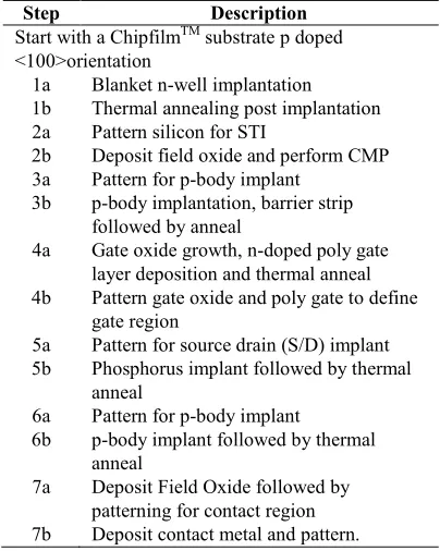
Table 1: Process Steps for Fabricating LDMOS
Step Description
Start with a ChipfilmTM substrate p doped
<100>orientation
1a Blanket n-well implantation 1b Thermal annealing post implantation 2a Pattern silicon for STI
2b Deposit field oxide and perform CMP 3a Pattern for p-body implant
3b p-body implantation, barrier strip followed by anneal
4a Gate oxide growth, n-doped poly gate layer deposition and thermal anneal 4b Pattern gate oxide and poly gate to define
gate region
5a Pattern for source drain (S/D) implant 5b Phosphorus implant followed by thermal
anneal
6a Pattern for p-body implant
6b p-body implant followed by thermal anneal
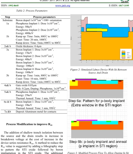
[image:2.612.326.528.478.731.2]ISSN: 1992-8645 www.jatit.org E-ISSN: 1817-3195
Table 2: Process Parameters
Step Process parameters
Substrate Boron doped 1x1014cm-3<100> orientation 1a Phosphorus Implant 1: Dose 1x1012cm-3,
Energy: 50keV
Phosphorus Implant 2: Dose 2x1012cm-3,
Energy: 400keV
1b Ramp up: Time: 5min, 800ºC to 1000ºC Coast: Time: 20 min, 1000ºC
Ramp down: Time: 5min,1000ºC to 800ºC 2a& b Oxide thickness: 0.4µm
3a Boron Implant 1: Dose 3x1012cm-3, Energy: 15keV
Boron Implant 2: Dose 3x1012cm-3,
Energy: 40keV
Boron Implant 3: Dose 3x1012cm-3, Energy: 100keV
Boron Implant 4: Dose 3x1012cm-3, Energy: 180keV
3b Ramp up: Time: 1min, 800ºC to 1000ºC Coast: Time: 10 min, 1000ºC
Ramp down: Time: 1min,1000ºC to 800ºC 4a& b Gate oxide 0.03µm
Poly: 0.2µm, Doping: Phosphorus, 1x1020cm-3 5a& b Phosphorus Implant 1: Dose 1x1015cm-3,
Energy: 25keV
Thermal Anneal: Time: 1 min, 950ºC 6a & b Boron Implant 1: Dose 1x1015cm-3,
Energy: 10keV
Thermal Anneal: Time: 1 min, 950ºC
7a &b Deposit Aluminum metal for contacts
Process Modification to improve Ron
The addition of shallow trench isolation between the source and the drain results in increase in breakdown voltage at the cost of increase in the
device series resistance Ron. A method to reduce the
Ron value is suggested by adding a lithography step
to pattern the STI oxide followed by boron implantation in the STI oxide. The additional process steps are elaborated in Figure 3.
3. PROCESS MODELING AND
SIMULATION
LDMOS fabrication process is modeled and simulated in a device simulation software package. The device structure is simulated using the process simulator and a device simulator is used for the performance simulation. The analytical models used for various processes and numerical computation are listed in Table .
[image:3.612.87.535.63.581.2]Figure 2: Simulated Ldmos Device With Sti Between Source And Drain
[image:3.612.312.528.639.709.2]Figure 3: Modified Process Flow To Allow Doping In Sti Region
Table 3: Process Models For Simulation
Process Model
Diffusion GAUSSIAN
Implantation PEARSON
Drift-diffusion solver GUMMEL, NEWTON
Mobility Lombarti CVT
Carrier generation & recombination Shockley-Reed Hall
ISSN: 1992-8645 www.jatit.org E-ISSN: 1817-3195 Mesh generation is an important step in the
device and process simulation. In the present structure meshing of varying densities is used. The mesh density is finer near the junctions and also near the gate oxide. The coarse mesh is used in the substrate and the bulk epitaxy. This helps in getting accurate solutions by solving large number of
computing nodes. Figure 4shows the meshingused
for the LDMOS device under consideration.
The device performance is simulated using a standard device simulator package. The basic drift-diffusion equations are solved to arrive at the device DC characteristics. Threshold voltage can be
extracted from the Id-Vg plot or using standard
commands available with the device simulator. The
Id-Vd characteristics of the device are also
simulated. The device breakdown voltage is simulated by sweeping the drain voltage and observing the drain current.
Figure 4: Meshing for the LDMOS device structure
4. RESULTSANDDISCUSSION
General Device Characteristics
[image:4.612.313.566.67.272.2]The device structure obtained from the process simulations described in Section II is shown in Figure 2. As discussed earlier, meshing defined for enabling the device simulation is shown in
Figure 4. The device doping profile in various
[image:4.612.313.564.309.482.2]regions is shown in Figure 5. This conforms to the defined LDMOS fabrication process. The p-body implant, source drain implants, the STI region and the epitaxial layer as defined in the process can be identified from Figure 2 and Figure 6. Gate oxide thickness of 30nm is achieved using the dry oxidation process as given in Table II.
[image:4.612.90.296.330.501.2]Figure 5: Simulated Ldmos Device Doping Profile For STI Device
Figure 6: Simulated LDMOS Device Doping Profile For Device With Boron Doping In STI
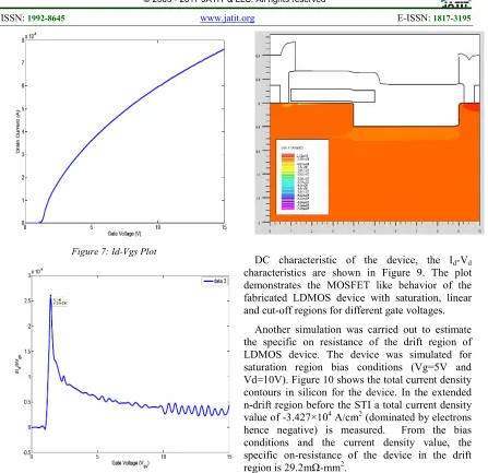
DC Characteristics
The DC characteristics of the device simulate the input and output characteristics. The output drain current for different gate and drain voltages is simulated. This gives a measure of the device threshold voltage. The Id-Vg characteristics of the
ISSN: 1992-8645 www.jatit.org E-ISSN: 1817-3195
Figure 7: Id-Vgs Plot
[image:5.612.90.300.534.709.2]Figure 8: Id-Vg slope. Maximum at Vg=1.46V
Figure 9: Id-Vd plot for different gate voltages
DC characteristic of the device, the Id-Vd
characteristics are shown in Figure 9. The plot demonstrates the MOSFET like behavior of the fabricated LDMOS device with saturation, linear and cut-off regions for different gate voltages.
Another simulation was carried out to estimate the specific on resistance of the drift region of LDMOS device. The device was simulated for saturation region bias conditions (Vg=5V and Vd=10V). Figure 10 shows the total current density contours in silicon for the device. In the extended n-drift region before the STI a total current density
value of -3.427×10⁴ A/cm2 (dominated by electrons
hence negative) is measured. From the bias conditions and the current density value, the specific on-resistance of the device in the drift
region is 29.2mΩ-mm2.
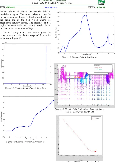
ISSN: 1992-8645 www.jatit.org E-ISSN: 1817-3195 device. Figure 13 shows the electric field in
breakdown regime. The same is shown across the device structure in Figure 4. The highest field is at the drain end of the STI region where the breakdown actually occurs. The presence of STI region between drain and source, results in an increase in the breakdown voltage.
The AC analysis for the device gives the transconductance plot for the range of frequencies as shown in Figure 25.
Figure 11: Simulated Breakdown Voltage Plot
Figure 12: Electric Potential At Breakdown
Figure 13: Electric Field At Breakdown
[image:6.612.90.564.52.720.2]Figure 14: Electric Field During Breakdown. Maximum Field Is At The Drain End Of STI.
ISSN: 1992-8645 www.jatit.org E-ISSN: 1817-3195
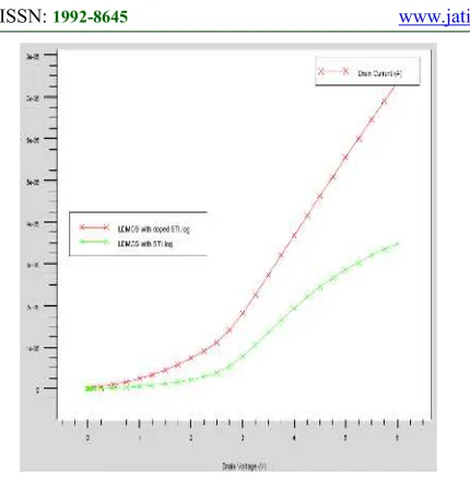
Figure 17: LDMOS Breakdown Voltage Comparison
16 show the comparison of Ron values for the device
with and without doping in the STI oxide region.
There is a two times improvement in the Ron value
by modifying the lithography step in the final p-body implant (Step 6). Moreover, the breakdown voltage is not affected by the proposed doping in the STI region (Fig 17).
Comparison notes
Performance comparisons of the proposed
LDMOS structure with existing structures
described in [6], [9], [10] and [11]. Breakdown
voltage and on resistance Ron is used for
comparisons.
In [6], using the high performance BCDMOS process from National Semiconductor’s i.e. PVIP25 LDMOS structures is developed. Performance of the conventional LDMOS structure developed using PVIP25 technology is reported. By
tuning the Chemical Mechanical
Polishing/Planarization (CMP) process, liner
oxidation and etching of silicon processes performance of LDMOS (both n-type and p-type) are improved. For comparison we only consider the n-type LDMOS described in [6].
In [10] using the standard High Voltage
0.18 CMOS technology a reduced surface field
(RESURF) LDMOS structure is developed. Varying dimensions of p-implant layer (PIL) and charge compensation techniques the performance of the conventional HVCMOS based (Maxchip Electronics Corporation) LDMOS is improved. Performance improvement is achieved without altering the standard process steps.
Using BIPOLAR-CMOS-DMOS (BCD)
technology from Richtek Technology Corporation in [11] low-to-medium voltage (6 to 60V) LDMOS transistor designs are presented. Using multi-oxide thickness techniques drift profile optimizations, reduction in power consumption and performance improvement over conventional LDMOS structures is reported.
The comparisons in terms of the breakdown voltage
and Ron are shown in Table I of the paper. In [6] the
best performance reported is of device New Etch + ISSG. The breakdown voltage of New Etch + ISSG [31] is lower by 46.29 % in comparison to our proposed LDMOS device. The breakdown voltage of our proposed device is improved by 14.81% over our previous device reported in [9]. In [10] the proposed LDMOS devices i.e. LDMOS (0.48µm ×3.0µm),LDMOS (0.48µm ×5.0µm), LDMOS (0.48µm ×8.0µm) show considerable improvement in comparison to the conventional device
represented as “Conventional HV
LDMOS”.Comparing our proposed LDMOS
structure with LDMOS structures proposed in [10],
higher breakdown voltage and comparable Ron
performance is reported. Authors in [11] have reported 36V DMOS and 45V DMOS [11]
structures exhibit best in class Ron performance
when compared to commercially available
conventional LDMOS devices offered by various fabrication houses. The proposed LDMOS has a 10.72% higher breakdown voltage when compared
to 36V DMOS [11] and Ron is reduced by 13.35%
in comparison to 45V DMOS [11]. The performance comparison results tabulated prove
that the proposed LDMOS exhibits best
performance considering both breakdown voltage and Ron.
Table IIv: Performance Comparisons Considering Breakdown Voltage And Ron
Device Name Breakdown
Voltage
Ron reported
POR [31] 29V 300 Ω
New Etch [31] 29V 277 Ω
New Etch + ISSG [31] 29V 277 Ω
Chipfilm LDMOS [34] 46 V -Not available-
Conventional HV LDMOS [35] 25.8 V 13.3 mΩ×mm2
LDMOS (0.48µm ×3.0µm) [35] 28.9 V 14.2 mΩ×mm2
LDMOS (0.48µm ×5.0µm) [35] 28.6 V 20.0 mΩ×mm2
LDMOS (0.48µm ×8.0µm) [35] 28.1 V 33.3 mΩ×mm2
6V DMOS [36] 14.3 V 3.7 mΩ×mm2
8V DMOS [36] 17 V 5.2 mΩ×mm2
17V DMOS [36] 27.2 V 8.7 mΩ×mm2
24V DMOS [36] 37.4 V 13 mΩ×mm2
36V DMOS [36] 48.2 V 22.9 mΩ×mm2
45V DMOS [36] 68 V 33.7 mΩ×mm2
Proposed LDMOS 54 V 29.2
[image:7.612.306.533.560.736.2]ISSN: 1992-8645 www.jatit.org E-ISSN: 1817-3195
5. CONCLUSIONANDFUTUREWORK
The present work is an extension to the previous work presented in [34]. The device process is altered to add a STI oxide region between drain and source with the aim of improving upon the breakdown voltage of the device.
The LDMOS process is modeled and the device structure is simulated for different operating characteristics.
The LDMOS device on ultra-thin substrates is a feasible structure and opening up numerous applications in the flexible electronic circuits. A CMOS compatible process flow is devised for device fabrication such that device fabrication can be carried out using the same process flow and along with the CMOS devices. High breakdown voltage LDMOS and CMOS devices can be fabricated on the same process.
The modeled device has an STI region between the drain and source region. The extended n-drift region is followed by the STI region which indeed helps in improving the device breakdown voltage. The same is depicted through the device simulations. A breakdown voltage of 54V is achieved using the STI layer. The device demonstrates normal characteristics of a MOSFET device with a threshold voltage of 1.46V.A specific
on resistance value of 29.2mΩ-mm2 is measured in
the extended n-drift region. Comparisons of our resistance with existing commercially available LDMOS devices prove performance improvements.
REFRENCES:
[1] Dye N, G. H. (2001). Radio Frequency
Transistors: Principles and Practical
Applications. Newness.
[2] F van Rijs, S. T. (2006). Efficiency
improvement of LDMOS transistors for base stations: towards the theoretical limit., (pp. 205-208).
[3] Rjis, F. V. (2008). Status and Trends of Silicon
LDMOS base station PA technologies to go
beyond 2.5GHz applications. RWS2008, (pp.
69-72)
[4] Sigg, H. J., Vendelin, G. D., Cauge, T. P., and
Kocsis, J.: D-MOS Transistor for Microwave applications, IEEE T. Electron Dev., ED-19(1), 45–53, 1972.
[5] Ludikhuize, A.W.: A review of RESURF
Technology, in: Proc. Int. ISPSD Conf. 2000, 11–18, 2000.
[6] Haynie S. Power LDMOS with novel STI
profile for improved Rsp, BVDSS, and reliability. ISPSD Hiroshima, pp-241-244, June 2010
[7] Chen, J.F.; Kuen-Shiuan Tian; Shiang-Yu
Chen; Kuo-Ming Wu; Liu, C.M.;, "On-Resistance Degradation Induced by Hot-Carrier Injection in LDMOS Transistors With STI in the Drift Region," Electron Device Letters, IEEE, vol.29, no.9, pp.1071-1073, Sept.2008
[8] A. Nezar and C. A. T. Salama "Breakdown
voltage in LDMOS transistor using internal
field rings", IEEE Trans. Electron Devices,
vol. 38, no. 7, pp.1676 -1680 1991
[9] Sunitha HD, Keshaveni N“Modeling and
Simulation of LDMOS Device” International Journal of Engineering Research, Vol 4, Issue 6, pp 291-295, 2015
[10]M. H. Han, H. B. Chen, C. J. Chang, C. C. Tsai
and C. Y. Chang, "Improving Breakdown Voltage of LDMOS Using a Novel Cost Effective Design," in IEEE Transactions on Semiconductor Manufacturing, vol. 26, no. 2, pp. 248-252, May 2013.
[11]T. Y. Huang et al., "0.18um BCD technology