Archive of SID
RESEARCH NOTE
GENERATION OF THREE-PHASE PWM INVERTER USING
XILINX FPGA AND ITS APPLICATION FOR UTILITY
CONNECTED PV SYSTEM
S. Mekhilef and N. A. Rahim
Power Electronics Research Laboratory, Department of Electrical Engineering University of Malaya, 50603 Kuala Lumpur, Malaysia, [email protected]
(Received: January 17, 2003 – Accepted in Revised Form: August 18, 2004)
Abstract Analysis and practical implementation of the regular symmetric sampled three-phase PWM inverter waveform has been presented in this paper. It is digitally implemented on a Xilinx field programmable gate array FPGA, and the essential considerations involved in the feasibility of using a Xilinx XC4008E software-based to generate PWM has been discussed. All the necessary Xilinx hardware/software techniques and programs required to implement and generate three-phase Pulse Width Modulation (PWM) are developed in detail, and demonstrated using practical results from an experimental Xilinx board. The techniques developed and presented in this paper are readily applicable to other currently available Xilinx chips. Simulation and experimental results of grid-connected inverter are presented. From the simulation and experimental results it is confirmed that the harmonic distortion of the output current waveform of the inverter fed to the grid is within the stipulated limits laid down by the utility companies.
Key Words Pulse Width Modulation (PWM), FPGA, Inverter, Photovoltaic (PV)
ﻩﺪﻴﻜﭼ
ﯽﻠﻤﻋﺩﺮﺑﺭﺎﮐﻭﯽﻤﻠﻋﻞﻴﻠﺤﺗ ﻪﻧﻮﻤﻧ
ﻝﺪﺒﻣ ﺝﻮﻣﻞﮑﺷ PWM
ﯽﻟﻮﻤﻌﻣﻥﺭﺎﻘﺘﻣﺯﺎﻓﻪﺳﻉﻮﻧ
ﻪـﻟﺎﻘﻣﻦـﻳﺍﺭﺩ
ﺖﺳﺍﻩﺪﺷﻪﺋﺍﺭﺍ
. ﺩﺮﺑﺭﺎﮐ
ﻝﺎﺘﻴﺠﻳﺩﻡﺮﻓﻪﺑﻪﻠﻴﺳﻭﻦﻳﺍ ﺑ
ﺮ
ﻪﻳﺍﺭﺁ
ﯼﺰﻳﺭﻪﻣﺎﻧﺮﺑﻞﺑﺎﻗ FPGA ﺎﺑ ﻥﺍﺪـﻴﻣ ﺲﮑﻨـﻴﻠﻳﺯ Xilinx ﻪﺑﺮﺠﺗ ﻭﻩﺪﻳﺩﺮﮔ ﻪﻣﺎﻧﺮﺑﯼﺮﻴﮔﺭﺎﮑﺑﻥﺎﮑﻣﺍ ﯼﺭﺍﺰﻓﺍﻡﺮﻧ Xilinx XC4008E ﺪﻴﻟﻮﺗﯼﺍﺮﺑ PWM ﺮﺑ ﺭ ﯽـﺳ ﺖـﺳﺍﻩﺪـﺷ . ﻤﻫ ﺔ ﯼﺭﻭﺎﻨﻓ
ﯼﺭﺍﺰﻓﺍﻡﺮﻧﻭﯼﺭﺍﺰﻓﺍﺖﺨﺳﯼﺎﻫ
ﯼﺭﻭﺮﺿ ﺲﮑﻨﻴﻠﻳﺯ
ﺪـﻴﻟﻮﺗﻭﯼﺮﻴﮔﺭﺎـﮑﺑﯼﺍﺮـﺑﻡﺯﻻﯼﺎـﻫﻪﻣﺎﻧﺮﺑﻭ
ﺯﺎﻓﻪﺳﻝﻭﺪﻣ
ﯼﺎﻨﻬﭘﺎﺑ ﭘﺎﻟ ﯽﺴ PWM ﻞﻴﺼﻔﺗﻪﺑ ﻪﺘﻓﺎﻳﻪﻌﺳﻮﺗ ﻭ
ﯽـﻠﻤﻋﺞﻳﺎـﺘﻧﺯﺍﻩﺩﺎﻔﺘﺳﺍﺎﺑ
ﮏـﻳﺯﺍﻞـﺻﺎﺣ
ﻪـﻧﻮﻤﻧ ﺲﮑﻨﻴﻠﻳﺯ ﯽﺸﻳﺎﻣﺯﺁ ﻪﺋﺍﺭﺍ ﻩﺪﺷ ﺖﺳﺍ . ﺭ ﻭ ﺵ ﯼﺎﻫ ﻪﺘﻓﺎﻳﻪﻌﺳﻮﺗ ﺩﺭﻮﻣ ﺚﺤﺑ ﺭﺩ ﻪـﻟﺎﻘﻣﻦـﻳﺍ
ﭗـﻴﭼﺮﻳﺎـﺳﯼﺍﺮـﺑ
ﯼﺎـﻫ ﯽﻟﻮﻤﻌﻣ ﻉﻮﻧ ﺲﮑﻨﻴﻠﻳﺯ ﺰﻴﻧ ﻪﺑ ﺳ ﺩﺎ ﮔ ﯽ ﻞﺑﺎﻗ ﻝﺎﻤﻋﺍ ﺖﺳﺍ . ﺞﻳﺎﺘﻧ
ﻭﯼﺯﺎﺳﻪﻴﺒﺷ
ﯽﺑﺮﺠﺗ ﯼﺎﻫﻝﺪﺒﻣ ﻣ ﮏﺒﺸ ﻞﺼـﺘﻣ ﺰـﻴﻧ ﺭﺩ ﻦﻳﺍ
ﺍﻩﺪﺷﻪﺋﺍﺭﺍﻪﻟﺎﻘﻣ ﺖﺳ . ﺞﻳﺎﺘﻧ ﻘﺤﺗ ﻴ ﻖ ﺩﺍﺩﻥﺎﺸﻧ ﻪﮐ
ﻥﺎﻳﺮﺟﮏﻴﻧﻮﻣﺭﺎﻫﺝﺎﺟﻮﻋﺍ
ﺝﻮـﻣ ﯽـﺟﻭﺮﺧ ﻝﺪـﺒﻣ ﻪـﻳﺬﻐﺗ ﻩﺪﺷ ﻞﺧﺍﺩﻪﺑ ﻣﻪﺤﻔﺻ ﮏﺒﺸ ﺪﺣﺭﺩ ﻝﻮﺒﻗﻞﺑﺎﻗ ﺖﮐﺮﺷ ﯼﺎﻫ ﺮﺑﺭﺎﮐ ﺍﺩﺭﺍﺮﻗ ﺖﺷ . 1. INTRODUCTION
The heart of any PWM control scheme is undoubtedly the switching strategy used to generate the switching edges of the PWM control waveform [1]. It is possible, by surveying the literature over the last decade to trace the historical development of PWM switching techniques and relate these developments to changes in technology, starting from analogue-based systems through discrete digital, and more recently ROM-based and microprocessor-implemented controls
schemes [2].
Archive of SID
2. PWM GENERATOR USING XILINX FPGA
FPGA is Programmable Logic Device developed by Xilinx, Inc. It comprises of thousand of logic gates. Some of them combined together to form a Configurable Logic Block (CLB). CLB simplifies higher-level circuit design. Gates interconnections using software are defined through SRAM or ROM. This provides flexibility to modify the designed circuit without altering the hardware part. Concurrent operation, less hardware, easy and fast circuit modification, comparatively low cost for a complex circuitry and rapid prototyping make it as the most favorable choice for prototyping an ASIC [5-7].
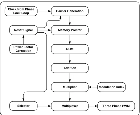
The overall block diagram of the three-phase PWM generator is shown in Figure 1. The carrier wave is compared with the multiplied modulating signal from the look-up table. The data of the look up table are stored in the internal ROM unit. The external multiplicand and the stored data will determine the modulation index of the PWM. The data stored in the look-up table (ROM) consists of 60 data from the Red phase and another 60 data from the Blue phase. Part of Yellow phase is derived using addition of Red and Blue phases. Selector Unit and Multiplexer are used to select the required signal to the appropriate channel as to form a proper PWM output pattern at the output terminals.
The shifting of signal waveform is essential in order to vary the power factor of the system. This is carried out by delay or advance the reset signal. The reset signal is tied up to the entire module. A positive triggering edge during positive and negative cycle is used as a reference by the reset signal. Advancing or delaying the reset signal by the external command will force the current in the main circuit to lead or lag the voltage supply.
2.1 Generation Modulating Wave Sinusoidal modulating waves are commonly used in PWM schemes, although other types of modulating wave, such as trapezoidal or triangular waves, have been employed in certain applications. The generation of a sine wave using Xilinx FPGA was done by storing the sine values in a lookup table, which is pre-programmed into permanent memory (ROM) the values having first been calculated [8].
T h e me mo r y r e q u i r e me n t , e f f i c i e n c y o f operation, and accuracy of the output waveform depends on the number of sample values defining a cycle of the sine wave and their resolution. If for example, the values are taken at 0.50 intervals, then a complete modulating cycle is defined by 720 values. The modulating wave could be defined at a greater number of sample points, but the memory requirement is proportionally increased. Hence, the point at which a sample is taken for the modulating process directly corresponds to a value in the lookup table. If a single-phase carrier is generated then each frequency ratio must be a multiple of three to eliminate the carrier frequency harmonics [9-10]. In this case 600 data are stored of two phase and the third is derived from.
2.1.1. Look-Up Table The sample of Red phase and Blue phase data, which are stored in the look-up table, are shown in below. The look-look-up tables are formed using the internal ROMs unit of Xilinx XC4008E.
; memfile COS.mem for LogiBLOX symbol rom1 ; Created on Saturday, July 14, 2002 16:47:55 ; Header Section
RADIX 10 DEPTH 256 WIDTH 8 DEFAULT 0 ; Data Section
Clock from Phase
Lock Loop Carrier Generation
Memory Pointer
ROM
Multiplier Modulation Index
Reset Signal
Power Factor Correction
Addition
[image:2.595.57.284.83.271.2]Selector Multiplexer Three Phase PWM
Archive of SID
; Specifies data to be stored in different addresses; e.g., DATA 0:A, 1:0 RADIX 10
DATA
22,22,21,21,21,21,20,20,20,20,19,19,19,18,18,18,17,17, 17,16,16,16,
15,15,15,14,14,14,13,13,12,12,12,11,11,10,10,10,9,9,8, 8,7,7,7,6,6,5,
5,4,4,4,3,3,2,2,1,1,0,0 ; end of LogiBLOX memfile
; memfile SIN.mem for LogiBLOX symbol ROM1 ; Created on Saturday, July 14, 2002 16:27:52 ;
; Header Section RADIX 10 DEPTH 256 WIDTH 8 DEFAULT 0 ;
; Data Section
; Specifies data to be stored in different addresses ; e.g., DATA 0:A, 1:0
RADIX 10 DATA
0,0,1,1,2,2,3,3,4,4,4,5,5,6,6,7,7,7,8,8,9,9,10,10,10,11,11 ,12,12,12,
13,13,14,14,14,15,15,15,16,16,16,17,17,17,18,18,18,19, 19,19,20,20,
20,20,21,21,21,21,22,22, ; end of LogiBLOX memfile
2.2 Triangular Carrier Generation The triangular carrier wave can be generated using up/down counter. The rate at which this counter is incremented (or decremented) determines the carrier frequency and accuracy of the sampling process. Each time the counter is incremented (or decremented), its output is compared with a sampled value of the modulating wave to determine the switching edge of the PWM waveform.
2 . 2 . 1 C a r r i e r F r e q u e n c y D e t e r m i n a t i o n Determination of carrier frequency is the first step of design process, where the clock frequency needs to be calculated precisely. The carrier frequency (fc) had been decided to operate at 18 kHz.
The decision was based on various factors such as inverter topology, acoustic radiation, type of power switching devices used and limitation of the peripheral components. Operating at high
frequency is better than the low frequency where the harmonic components could be shifted to high order. However at high frequency more switching stress and power losses occur in the devices especially in the three devices controlled bridge topology.
The carrier frequency has a relationship with the main clock frequency and the up-down counter that could be expressed as:
fc = fclk/[2(2 n
-1)] (1)
Where fc is the carrier frequency, fclk is the main
clock frequency and n is the bit size of the up-down counter.
2.2.2. Determination of Main Clock Signal An 8-bit up-down counter must be clocked at 9.18MHz to produce 18kHz carrier frequency according to Equation 1. The clock signal is locked and synchronized with the AC mains frequency of 50Hz by using an external phase-locked loop circuitry. The division of clock frequency from 9.18MHz to 50Hz is accomplished by using internal counter in the Xilinx chip. The 50Hz feedback frequency is used as an input to the phase-locked loop (PLL) chip to lock the phase with the supply phase reference voltage.
3. INVERTER CONFIGURATION
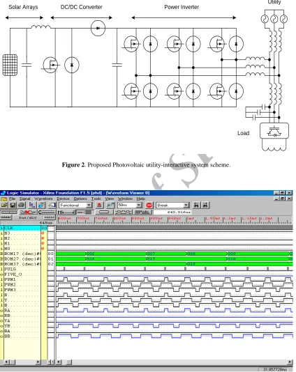
Figure 2 shows the schematic description of a PV utility-interactive system. The power Inverter is primarily responsible for converting the DC PV power into utility compatible AC power and for synchronizing and transferring that AC power safely into the utility grid.
Archive of SID
4. RESULTS
The selected results have been chosen to illustrate
some of the main features of the new three-phase Pulse Width Modulation (PWM) generated using Xilinx XC4008E. Simulation is performed using
Solar Arrays DC/DC Converter Power Inverter Utility
Load
[image:4.595.88.512.91.625.2]Figure 2. Proposed Photovoltaic utility-interactive system scheme.
Archive of SID
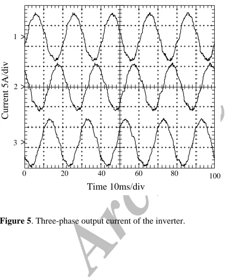
[image:5.595.58.282.87.242.2]the 1.5 foundation series in Figure 3 the simulation of three-phase PWM inverter is shown applied to the six switches of the inverter scheme whereas Figure 4 shows the six PWM waveforms generated using Xilinx XC4008E each one is applied to one IGBT in the power circuit. Figure 5 shows the three-phase output current of the inverter using low pass filter.
5. CONCLUSION
Using Xilinx FPGA to generate the PWM provides flexibility to modify the designed circuit without altering the hardware part. Concurrent operation, less hardware, easy and fast circuit modification, comparatively low cost for a complex circuitry and rapid prototyping make it as the most favorable choice for the PWM generation. From the simulation and experimental results it is confirmed that the harmonic distortion of the output current waveform of the inverter fed to the grid is within the stipulated limits laid down by the utility companies, the THD is less than 5%.All the above advantages have made the inverter configuration highly suitable for grid connected photovoltaic application (5kW).
6. REFERENCES
1. Rahim, N. A., Green, T. C. and Williams, B. W., “PWM ASIC Design for the Three-Phase Bi-directional Buck Converter”, International Journal of Electronics, Vol. 81, No. 5, (1996), 603-615.
2. Holtz, J. “Pulse Width Modulation for Power Electronic Power Conversion”, Proceedings of the IEEE, Vol. 82, No. 8, (August 1994), 1194-1214.
3. Makhlief, S., Rahim, N. A. and Omar, A. M., “Microprocessor Implementation of Three Phase PWM Switching Strategies”, IEEE 1999 International Conference On Power Electronics And Drive System,
PEDS’99, Hong Kong, Vol. 2, (July 1999), 161-166. 4. Bowes, S. R. and Clark, P. R., “Novel Microprocessor of
New Regular-Sampled Harmonic-Elimination PWM Techniques for Drives and Static- Power Converters”,
Intelligent Motion, June 1990 Proceeding, (June 1990), 175 – 180.
5. Biswas, S. K., Basak, B. and Swamy, M. M., “A Three-Phase Half Controlled Rectifier with Pulse Width Modulation”, IEEE Transactions on Industrial Electronics, Vol. 38, No. 2, (April 1991), 122 – 125. 6. Mechi, A. and Funabiki, S. “Step-up Voltage PWM
AC to DC Converter With One Switching Device”,
IEE Proceedings B, Vol. 140, No.1, (January 1993), 35 – 40.
7. Mirkazemi-Moud, M., Williams, B. W. and Green, T. C., “Use of Asic Technology in the Design of Two Novel PWM Generators”, Fourth International Conference on Power Electronics and Variable Speed Drive 1991, (1991), 347-352.
8. Grant,R.Seidner, D. A., “Ratio Changing in Pulse-Width-Modulated Inverter”, IEE Proceeding, Vol. 128, Pt. B, No. 5, (September 1981), 243 - 248.
9. Bowes, S. R. and Midoun, A., “Suboptimal Switching Strategies for Microprocessor Controlled PWM Inverter
0 >
0 >
0 >
4 >
0 >
0 >
0 >
10 20 30 40
time, mS (5ms/div)
Volt,
V (10V/div)
Phase A
Phase B
Phase C
S1
S6 S3 S5 S2 S4
>
>
[image:5.595.57.288.324.608.2]> > > >
Figure 4. Three-phase PWM generated using XC4008E.
C
u
rrent 5A
/div
Time 10ms/div
100 80
60 40
0 20
1
2
3
Archive of SID
Drives”, IEE Proceedings, Vol. 132, Pt B, No. 3, (May 1985), 133 – 148.
10. Yu, Z., Mohammed, A. AND Panaphi, I., “A Review of